

SGS Thomson Microelectronics STB55NF03L Datasheet
STB55NF03L
N-CHANNEL 30V - 0.01
TYPE V
ST B55NF03L 30 V < 0. 013 Ω 55 A
■ TYPICALR
■ OPTIMIMIZEDFOR HIGH SWITCHING
DS(on)
DSS
= 0.01 Ω
OPERATIONS
■ LOW GATE CHARGE
■ LOGICLEVEL GATE DRIVE
DESCRIPTION
This Power Mosfet is the latest development of
STMicroelectronics unique ”Single Feature
Size” strip-basedprocess. The resulting transistor shows extremely high packing density forlow
on-resistance, rugged avalance characteristics
and less critical alignment steps therefore a remarkablemanufacturingreproducibility.
APPLICATIONS
■ LOW VOLTAGEDC-DC CONVERTERS
■ HIGHCURRENT, HIGHSPEED SWITCHING
■ HIGHEFFICIENCY SWITCHINGCIRCUITS
R
DS(on)
I
D
Ω
- 55A D2PAK
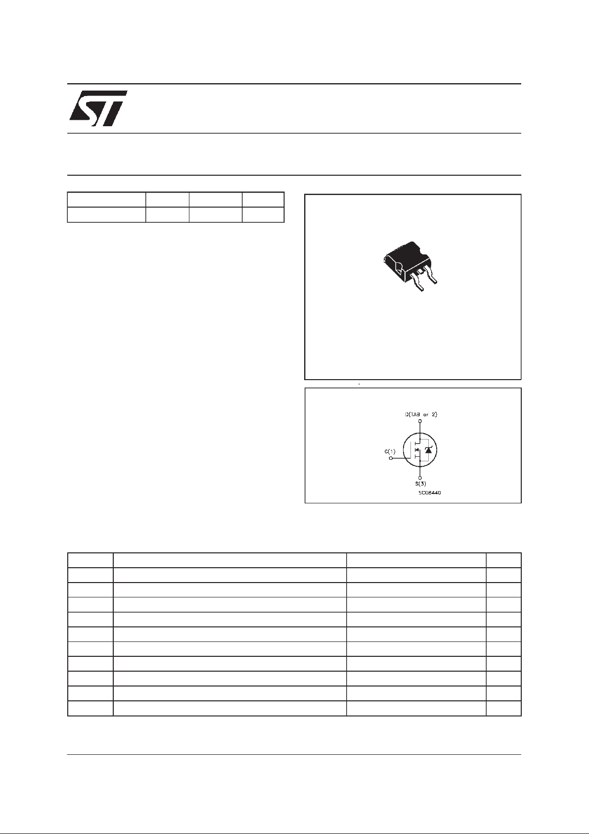
STripFET POWER MOSFET
3
1
D2PAK
TO-263
ADD SUFFIX ”T4”FOR ORDERING INTAPE & REEL
INTERNAL SCHEMATIC DIAGRAM
ABSOLUTE MAXIMUM RATINGS
Symbol Parameter Value Unit
V
V
V
I
DM
P
T
(•) Pulsewidth limited by safeoperating area
10/01/2000
Dra in- sour c e Volt age (VGS=0) 30 V
DS
Dra in- gate Volt age (RGS=20kΩ)30V
DGR
Gat e-source Voltage
GS
I
Dra in Current (c ont in uous ) at Tc=25oC55A
D
I
Dra in Current (c ont in uous ) at Tc=100oC39A
D
(•) D rain Cu rr ent (p ulsed) 220 A
Tot al Dissipation at Tc=25oC80W
tot
Der ati ng Fac t or 0.53 W/
St orage Tem pe rat ure -65 to 175
stg
T
Max. Operating Junct ion Temper at ur e 175
j
20 V
±
o
C
o
C
o
C
1/8
STB55NF03L
THERMAL DATA
R
thj-case
R
thj-amb
T
Ther mal Resistanc e Junct ion-case Max
Ther mal Resistanc e Junct ion-ambient Max
Maximum Lead T emperat ur e For Soldering Purpose
l
1.875
62.5
300
o
C/W
o
C/W
o
C
ELECTRICAL CHARACTERISTICS
=25oC unless otherwisespecified)
(T
case
OFF
Symbol Parameter Test Conditions Min. Typ. Max. U nit
V
(BR)DSS
Drain-source
ID=250µAVGS=0 30 V
Break dow n Voltage
I
DSS
I
GSS
Zero Gate Voltage
Drain Current (V
GS
Gat e- bod y Leakage
Current (V
DS
=0)
=0)
V
=MaxRating
DS
=MaxRating Tc=125oC
V
DS
V
= ± 20 V ± 100 nA
GS
1
10
ON(∗)
Symbol Parameter Test Conditions Min. Typ. Max. U nit
V
GS(th)
R
DS(on)
I
D(on)
Gate Threshold Voltage VDS=VGSID= 250 µA12.5V
Sta t ic Dr ain -s ource O n
Resistance
On State Drain Current VDS>I
VGS=10V ID=27.5A
V
=4.5V ID=27.5A
GS
D(on)xRDS(on)max
0.01
0.015
0.013
0.021
55 A
VGS=10V
DYNAMIC
Symbol Parameter Test Con ditions Min. Typ. Max. Unit
g
(∗)Forward
fs
Tr ansc on duc tance
C
C
C
Input C apac i t ance
iss
Out put Capacitanc e
oss
Reverse T r ansfer
rss
Capacit a nc e
VDS>I
D(on)xRDS(on)maxID
=27. 5 A 40 S
VDS=25V f=1MHz VGS= 0 1450
390
150
µA
µ
Ω
Ω
pF
pF
pF
A
2/8
STB55NF03L
ELECTRICAL CHARACTERISTICS
(continued)
SWITCHINGON
Symbol Parameter Test Con ditions Min. Typ. Max. Unit
t
d(on)
t
Tur n-on Delay Time
Rise T i me
r
VDD=15V ID= 27.5 A
R
=4.7
G
Ω
VGS=4.5V
25
280
(Resis t iv e Load, see f ig. 3)
Q
Q
Q
Tot al G at e Char ge
g
Gat e- Source Char g e
gs
Gate-Drain Charge
gd
VDD=24V ID=55A VGS=4.5V 25
11
12
35 nC
SWITCHINGOFF
Symbol Parameter Test Con ditions Min. Typ. Max. Unit
t
d(off)
Tur n-of f Delay Time
t
Fall T ime
f
VDD=15V ID= 27.5 A
=4.7 Ω VGS=4.5V
R
G
40
60
(Resis t iv e Load, see f ig. 3)
SOURCEDRAINDIODE
Symbol Parameter Test Con ditions Min. Typ. Max. Unit
I
SD
I
SDM
V
SD
t
Q
I
RRM
(∗) Pulsed: Pulse duration = 300µs, duty cycle 1.5 %
(•) Pulse width limited by safe operating area
Source-drain Current
(•)
Source-drain Current
55
220
(pulsed)
(∗)ForwardOnVoltage ISD=55A VGS=0 1.3 V
Reverse Re covery
rr
Time
Reverse Re covery
rr
ISD= 55 A di/dt = 100 A/µs
=15V Tj=150oC
V
DD
(see test circuit, fig. 5)
45
52
Charge
Reverse Re covery
2.3
Current
ns
ns
nC
nC
ns
ns
A
A
ns
nC
A
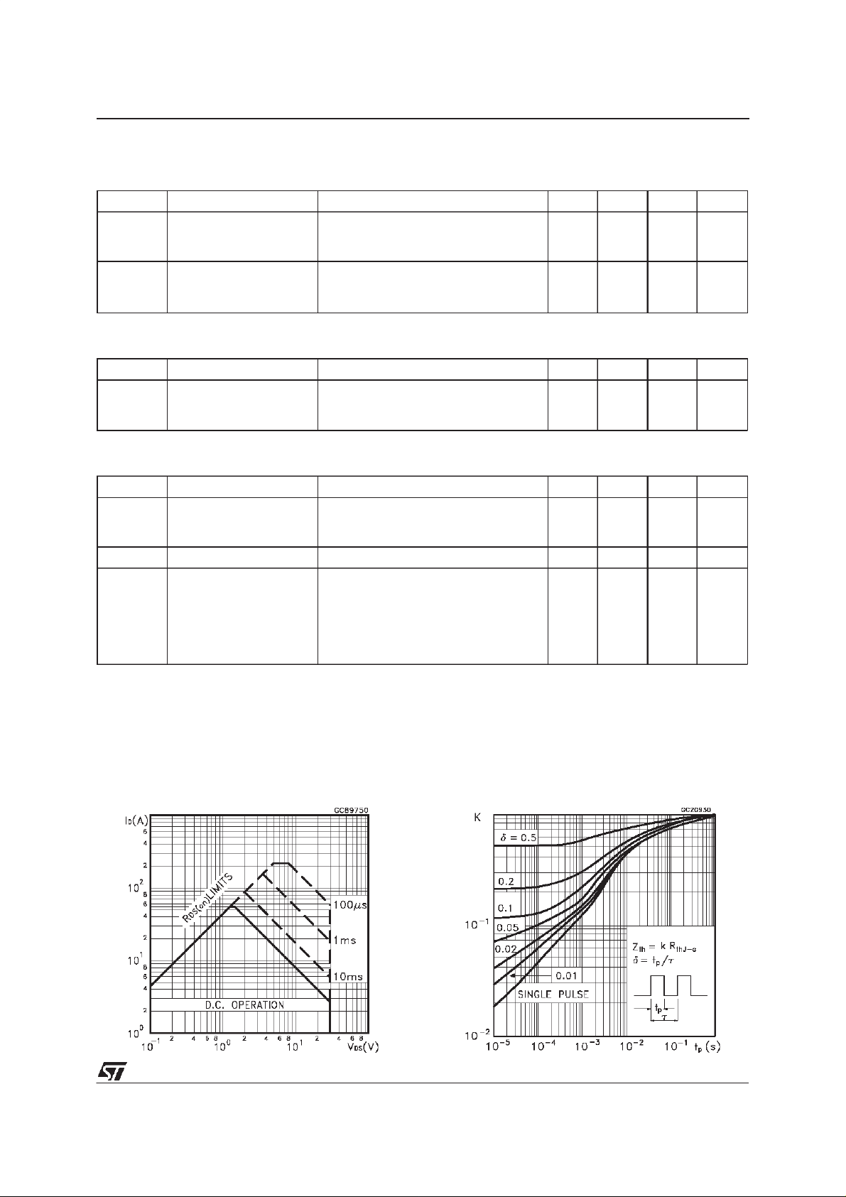
SafeOperating Area ThermalImpedance
3/8
 Loading...