

SGS Thomson Microelectronics STB4NB80 Datasheet
®
N - CHANNEL 800V - 3Ω - 4A - TO -220/TO-220FP
TYPE V
STB4NB80
STB4NB80FP
■ TYPICAL R
■ EXTREME LY HIGH dv/dt CAP A BI LIT Y
■ 100% AVALANCHE TESTED
■ VERY LOW INTRINSIC CAPACITANCES
■ GATE CHARGE MINIMIZED
DS(on)
DSS
800 V
800 V
= 3 Ω
DESCRIPTION
Using the latest high voltage MESH OVERLAY
process, SGS-Thomson has designed an
advanced family of power MOSFETs with
outstanding performances. The new patent
pending strip layout coupled with the Company’s
proprietary edge termination structure, gives the
lowest RDS(on) per area, exceptional avalanche
and dv/dt capabilities and unrivalled gate charge
and switching char acteristics.
R
DS(on)
3.3 Ω
3.3 Ω
I
D
4 A
4 A
STB4NB80
PowerMESH MOSFET
PRELIMINARY DATA
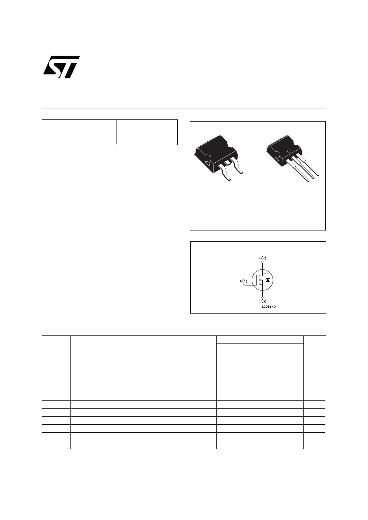
3
1
2
D
PAK
TO-263
(Suffix "T4")
INTER NAL SCH E M ATI C DIAG RA M
I2PAK
TO-262
(Suffix "-1")
3
2
1
APPLICATIONS
■ HIGH CURRENT, HIGH SPE ED SWI TCHING
■ SWITC H MODE POWER SU PPLIES ( SMPS)
■ DC-AC CONVE RTERS FOR WELDING
EQUIPMENT AND UNINTERRUPTIBLE
POWER SUPPLIES AND MOTOR DRIVE
ABSOLUTE MAXIMUM RATINGS
Symbol Parameter Value Unit
STB4NB80 STB4NB80FP
V
V
V
I
DM
P
dv/dt(1) Peak Diode Recovery voltage slope 4.5 4.5 V/ns
V
T
(•) Pulse width limited by safe operating area (1) ISD ≤4 A, di/dt ≤ 200 A/µs, VDD ≤ V
(*) Limited only by maximum temperature allowed
June 1998
Drain-source Voltage (VGS = 0) 800 V
DS
Drain- gate Voltage (RGS = 20 kΩ)
DGR
Gate-source Voltage ± 30 V
GS
I
Drain Current (continuous) at Tc = 25 oC 4 4(*) A
D
Drain Current (continuous) at Tc = 100 oC 2.4 2.4(*) A
I
D
800 V
(•) Drain Current (pulsed) 16 16 A
Total Dissipation at Tc = 25 oC10035W
tot
Derating Factor 1 0.28 W/
Insulation Withstand Voltage (DC) 2000 V
ISO
Storage Temperature -65 to 150
stg
Max. Operating Junction Temperature 150
T
j
, Tj ≤ T
(BR)DSS
JMAX
o
C
o
C
o
C
1/6
STB4NB80
THERMAL DATA
TO-263 TO-262
R
thj-case
R
thj-amb
R
thc-sink
T
AVALANCHE CHARACTERI S TICS
Symbol Parameter Max Value Unit
I
AR
E
Thermal Resistance Junction-case Max 1 3.6
Thermal Resistance Junction-ambient Max
Thermal Resistance Case-sink Typ
Maximum Lead Temperature For Soldering Purpose
l
Avalanche Current, Repetitive or Not-Repetitive
(pulse width limited by T
Single Pulse Avalanche Energy
AS
(starting T
= 25 oC, ID = IAR, V
j
ma x)
j
DD
= 50 V)
62.5
0.5
300
4A
230 mJ
o
C/W
o
C/W
o
C/W
o
C
ELECTRICAL CHARACTERISTICS (T
= 25 oC unless otherwise specified)
case
OFF
Symbol Parameter Test Conditions Min. Typ. Max. Unit
V
(BR)DSS
Drain-source
I
= 250 µA V
D
GS
= 0
800 V
Breakdown Voltage
I
DSS
I
GSS
Zero Gate Voltage
Drain Current (V
GS
Gate-body Leakage
Current (V
DS
= 0)
= 0)
= Max Rating
V
DS
V
= Max Rating Tc = 125 oC
DS
V
= ± 30 V
GS
1
50
± 100 nA
ON (∗)
Symbol Parameter Test Conditions Min. Typ. Max. Unit
V
GS(th)
Gate Threshold
V
= VGS ID = 250 µA
DS
345V
Voltage
R
DS(on)
Static Drain-source On
VGS = 10V ID = 2 A 3 3.3 Ω
Resistance
I
D(on)
On State Drain Current VDS > I
V
= 10 V
GS
D(on)
x R
DS(on)max
4A
DYNAMIC
Symbol Parameter Test Conditions Min. Typ. Max. Unit
gfs (∗) Forward
Transconductance
C
C
C
Input Capacitance
iss
Output Capacitance
oss
Reverse Transfer
rss
Capacitance
VDS > I
V
DS
x R
D(on)
DS(on)max
= 25 V f = 1 MHz V
ID = 2 A 1.8 S
= 0 700
GS
95
920
126
9
12
µA
µA
pF
pF
pF
2/6
 Loading...