

SGS Thomson Microelectronics STB40NS15 Datasheet
STB40NS15
N-CHANNEL 150V - 0.042Ω - 40A D2PAK
MESH OVERLAY™ MOSFET
PRELIMINARY DATA
TYPE V
DSS
R
DS(on)
I
D
STB40NS15 150 V <0.052Ω 40A
■ TYPICAL R
■ EXTREMELY HIGH dv /d t C APABILITY
■ VERY LOW INTRINSIC C APAC ITANCES
■ GATE CHARGE MINIMIZED
(on) = 0.042Ω
DS
DESCRIPTION
This powermos MOSFET is designed using the
company’s consolidated strip layout-based MESH
OVERLAY
™ process. This technology matches
and improves the performances compared with
standard parts from various sources.
APPLICATIONS
■ HIGH CURRENT SWITCHING
■ UNINTERRUPTIBLE POWER SUPPLY (UPS)
■ PRIMARYSWITCH IN ISOLATED DC-DC
CONVERTERS
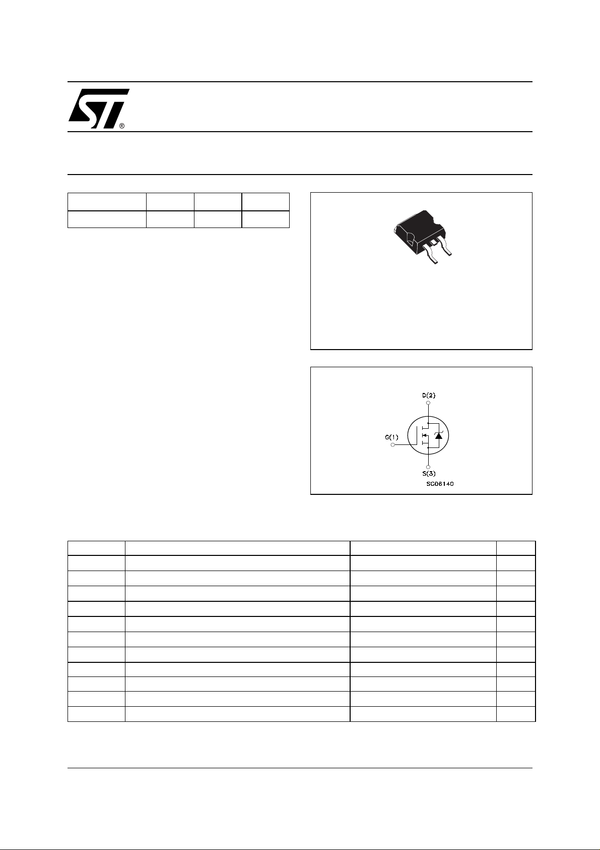
3
1
D2PAK
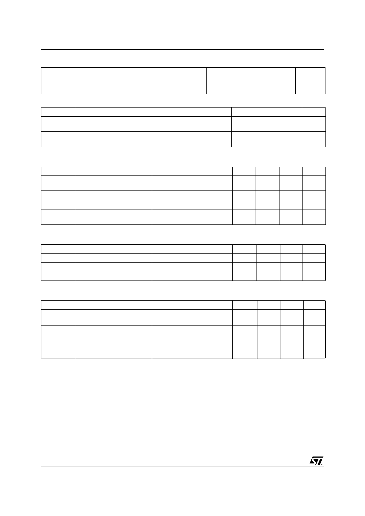
I
NTERNAL SCHEMATIC DIAGRAM
ABSOLUTE MAXIMUM RATINGS
Symbol Parameter Value Unit
V
DS
V
DGR
V
GS
I
D
I
D
I
DM
P
TOT
dv/dt Peak Diode Recovery voltage slope 9 V/ns
T
stg
T
j
(•)Pu l se width limited by safe operating area
December 2001
This is preliminary information on a new product now in development or undergoing evaluation. Details are subject to change without notice.
Drain-source Voltage (VGS = 0)
Drain-gate Voltage (RGS = 20 kΩ)
150 V
150 V
Gate- source Voltage ±20 V
Drain Current (continuos) at TC = 25°C
Drain Current (continuos) at TC = 100°C
(●)
Drain Current (pulsed) 160 A
Total Dissipation at TC = 25°C
40 A
25 A
140 W
Derating Factor 0.933 W/°C
Storage Temperature –65 to 175 °C
Max. Operating Junction Temperature 175 °C
1/7
STB40NS15
THERMA L D ATA
Rthj-case Thermal Resistance Junction-case Max 1.07 °C/W
Rthj-amb Thermal Resistance Junction-ambient Max 62.5 °C/W
T
l
AVALANCHE CHARACTERISTICS
Symbol Parameter Max Value Unit
I
AR
E
AS
ELECTRICAL CHARACTERISTICS (TCASE = 25 °C UNLESS OTHERWISE SPECIFIED)
OFF
Symbol Parameter Test Conditions Min. Typ. Max. Unit
V
(BR)DSS
I
DSS
I
GSS
Maximum Lead Temperature For Soldering Purpose 300 °C
Avalanche Current, Repetitive or Not-Repetitive
(pulse width limited by T
max)
j
Single Pulse Avalanche Energy
(starting T
Drain-source
= 25 °C, ID = IAR, VDD = 50 V)
j
ID = 250 µA, VGS = 0 150 V
40 A
500 mJ
Breakdown Voltage
Zero Gate Voltage
Drain Current (V
GS
Gate-body Leakage
Current (V
DS
= 0)
= 0)
V
= Max Rating
DS
V
= Max Rating, TC = 125 °C
DS
V
= ±20V ±100 nA
GS
1µA
10 µA
ON
(1)
Symbol Parameter Test Conditions Min. Typ. Max. Unit
V
GS(th)
R
DS(on)
Gate Threshold Voltage
Static Drain-source On
V
= VGS, ID = 250µA
DS
VGS = 10V, ID = 40 A
234V
0.044 0.052 Ω
Resistance
DYNAMIC
Symbol Parameter Test Conditions Min. Typ. Max. Unit
(1) Forward Transconductance VDS > I
g
fs
C
iss
C
oss
C
rss
Input Capacitance
Output Capacitance 380 pF
Reverse Transfer
Capacitance
I
D
V
= 20A
DS
D(on)
x R
DS(on)max,
= 25V, f = 1 MHz, VGS = 0
20 S
2400 pF
160 pF
2/7
STB40NS15
ELECTRICAL CHARACTERISTICS (CONTINUED)
SWITCHING ON
Symbol Parameter Test Conditions Min. Typ. Max. Unit
t
d(on)
t
r
Q
Q
gs
Q
gd
g
Turn-on Delay Time
Rise Time
Total Gate Charge VDD = 120V, ID = 40A,
Gate-Source Charge 17 nC
Gate-Drain Charge 47 nC
SWITCHING OFF
Symbol Parameter Test Conditions Min. Typ. Max. Unit
t
d(off)
T
t
r(Voff)
t
t
f
f
c
Turn-off Delay Time
Fall Time
Off-voltage Rise Time
Fall Time
Cross-over Time
= 75V, ID = 20A
V
DD
RG= 4.7Ω, VGS = 10V
(see test circuit, Figure 3)
VGS = 10V
V
= 75V, ID = 20A
DD
R
=4.7Ω, VGS = 10V
G
(see test circuit, Figure 3)
V
= 120V, ID = 20 A,
clamp
RG=4.7Ω, V
GS
= 10V
(see test circuit, Figure 5)
25 ns
45 ns
100 110 nC
85 ns
47
35
70
ns
ns
ns
SOURCE DRAIN DIODE
Symbol Parameter Test Conditions Min. Typ. Max. Unit
I
SD
I
SDM
V
(1)
SD
t
rr
Q
rr
I
RRM
Note: 1. Pulsed: Pu l se duration = 300 µs, duty c yc l e 1.5 %.
2. Pulse width li mited by safe operating area.
Source-drain Current 40 A
(2)
Source-drain Current (pulsed) 160 A
Forward On Voltage
Reverse Recovery Time
Reverse Recovery Charge
Reverse Recovery Current
ISD = 40A, VGS = 0
= 40A, di/dt = 100A/µs,
I
SD
VDD = 50V, Tj = 150°C
(see test circuit, Figure 5)
270
200
1.5
1.5 V
ns
nC
A
3/7
 Loading...