

SGS Thomson Microelectronics STB40NF10-1 Datasheet
STP40NF10
STB40NF10 - STB40NF10-1
N-CHANNEL 100V - 0.024Ω - 50A TO-220/D2PAK/I2PAK
LOW GATE CHARGE STripFET™ II POWER MOSFET
TYPE V
STP40NF10
STB40NF10
STB40NF10-1
■ TYPICAL R
■ EXCEPTIONA L dv/d t CAPABILITY
■ 100% AVALANCHE TESTED
■ APPLICATION ORIENTED
DS
DSS
100 V
100 V
100 V
(on) = 0.024Ω
R
DS(on)
< 0.028 Ω
< 0.028 Ω
< 0.028 Ω
I
D
50 A
50 A
50 A
CHARACTERIZATION
■ ADD SUFFIX “T4” FOR ORDERING IN TAPE &
REEL
DESCRIPTION
This Power MOSFET series realized with STM icroelectronics unique STripFET process has specifically been designed to minimize input capacitance and
gate charge. It is therefore suitable as primary
switch in advanced high-efficiency isolated D C-DC
converters for T el ecom and Computer application. It
is also intended for any application with low gate
charge drive requirements.
APPLICATIONS
■ HIGH-EFFICIENCY DC-DC CONVERTERS
■ UPS AND MOTOR CONTROL
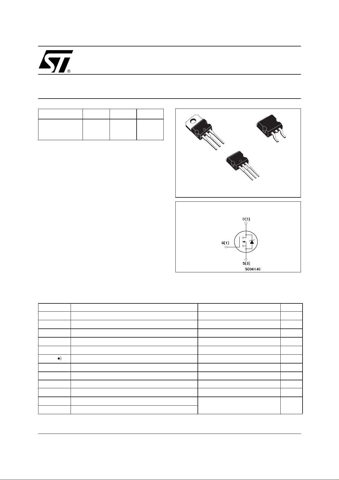
3
2
1
1
D2PAK
TO-220
3
2
1
I2PAK
INTERNAL SCHEMATIC DIAGRAM
3
ABSOLUTE MAXIMUM RATINGS
Symbol Parameter Value Unit
V
DS
V
DGR
V
GS
I
(*) Drain Current (continuous) at TC = 25°C
D
I
D
I
DM
P
TOT
dv/dt (1) Peak Diode Recovery voltage slope 20 V/ns
E
AS
T
stg
T
j
(●) Pulse width limited by safe operating area
(*) Limited by Package
Drain-source Voltage (VGS = 0)
Drain-gate Voltage (RGS = 20 kΩ)
100 V
100 V
Gate- source Voltage ± 20 V
50 A
Drain Current (continuous) at TC = 100°C
(l)
Drain Current (pulsed) 200 A
Total Dissipation at TC = 25°C
35 A
150 W
Derating Factor 1 W/°C
(2)
Single Pulse Avalanche Energy 150 mJ
Storage Temperature
Operating Junction Temperature
(1) ISD ≤40A, di/dt ≤600A/µs, VDD ≤ V
(2) Starting Tj = 25°C, ID = 40A, VDD = 50V
– 55 to 175 °C
(BR)DSS
, Tj ≤ T
JMAX.
1/11September 2002
STP40NF10 - STB40NF10 - STB40NF10-1
THERMA L D ATA
Rthj-case Thermal Resistance Junction-case Max 1 °C/W
Rthj-amb Thermal Resistance Junction-ambient Max 62.5 °C/W
T
l
Maximum Lead Temperature For Soldering Purpose 300 °C
ELECTRICAL CHARACTERISTICS (T
= 25 °C UNLESS OTHERWISE SPECIFIED)
CASE
OFF
Symbol Parameter Test Conditions Min. Typ. Max. Unit
V
(BR)DSS
Drain-source
ID = 250 µA, VGS = 0 100 V
Breakdown Voltage
V
= Max Rating
DS
V
= Max Rating, TC = 125 °C
DS
V
= ± 20V ±100 nA
GS
1µA
10 µA
ON
I
I
GSS
(1)
DSS
Zero Gate Voltage
Drain Current (V
GS
Gate-body Leakage
Current (V
DS
= 0)
= 0)
Symbol Parameter Test Conditions Min. Typ. Max. Unit
V
V
GS(th)
R
DS(on)
Gate Threshold Voltage
Static Drain-source On
= VGS, ID = 250µA
DS
VGS = 10V, ID = 20 A
2 2.8 4 V
0.024 0.028 Ω
Resistance
DYNAMIC
Symbol Parameter Test Conditions Min. Typ. Max. Unit
(1) Forward Transconductance VDS = 25V, ID= 20 A 20 S
g
fs
C
iss
C
oss
C
rss
Input Capacitance
Output Capacitance 265 pF
Reverse Transfer
Capacitance
V
= 25V, f = 1 MHz, VGS = 0
DS
1780 pF
112 pF
2/11
STP40NF10 - STB40NF10 - STB40NF10-1
ELECTRICAL CHARACTERISTICS (CONTINUED)
SWITCHING ON
Symbol Parameter Test Conditions Min. Typ. Max. Unit
V
t
d(on)
Q
Q
Q
t
r
g
gs
gd
Turn-on Delay Time
Rise Time 63 ns
Total Gate Charge VDD = 80V, ID =40A,VGS = 10V 60
Gate-Source Charge 10 nC
Gate-Drain Charge 23 nC
SWITCHING OFF
Symbol Parameter Test Conditions Min. Typ. Max. Unit
t
d(off)
t
f
Turn-off-Delay Time
Fall Time
SOURCE DRAIN DIODE
Symbol Parameter Test Conditions Min. Typ. Max. Unit
I
SD
I
SDM
VSD (1)
t
rr
Q
rr
I
RRM
Note: 1. Pulsed: Pu l se duration = 300 µs, duty c ycle 1.5 %.
2. Pulse width li mited by safe operating area.
Source-drain Current 40 A
(2)
Source-drain Current (pulsed) 160 A
Forward On Voltage
Reverse Recovery Time
Reverse Recovery Charge
Reverse Recovery Current
= 50 V, ID = 20 A
DD
R
= 4.7Ω VGS = 10V
G
(see test circuit, Figure 3)
VDD = 50 V, ID = 20 A,
RG=4.7Ω, V
GS
= 10V
(see test circuit, Figure 3)
ISD = 40 A, VGS = 0
= 40 A, di/dt = 100A/µs,
I
SD
VDD = 25V, Tj = 150°C
(see test circuit, Figure 5)
28 ns
80
84
28
1.3 V
114
456
8
nC
ns
ns
ns
nC
A
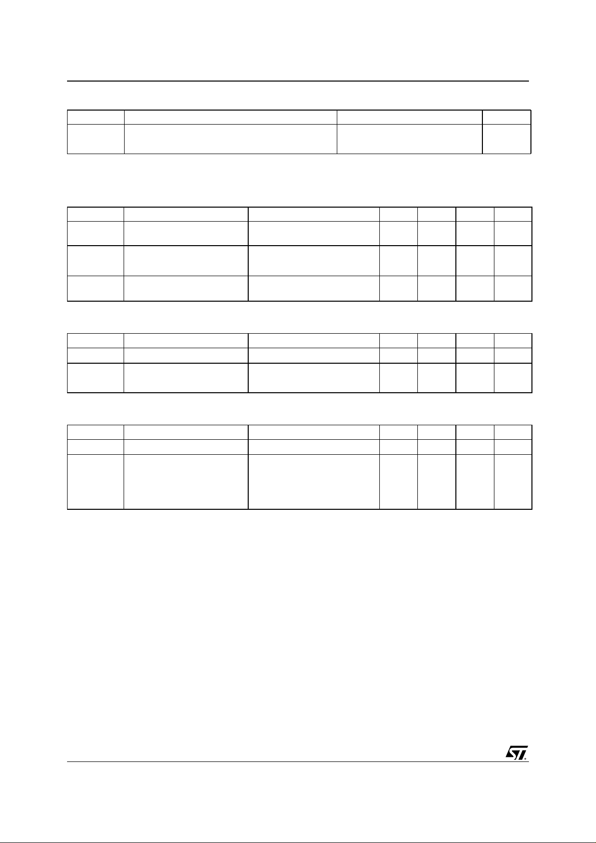
Thermal Impedance Safe Operating Area
3/11
STP40NF10 - STB40NF10 - STB40NF10-1
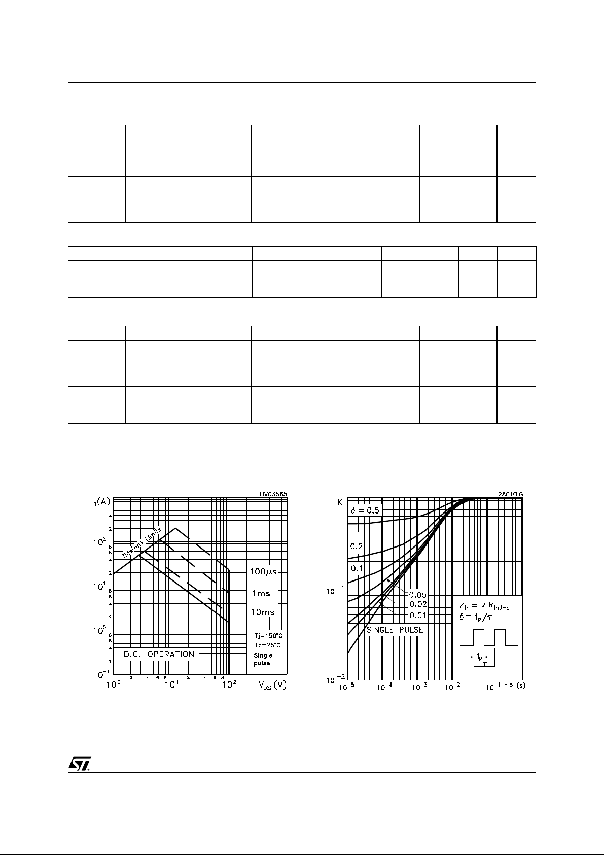
Output Characteristics
Transfer Characteristics
Static Drain-source On ResistanceTransconductanc e
Gate Charge vs Gate-source Voltage
4/11
Capacitance Variations
 Loading...