

N - CHANNEL 100V- 0.030Ω - 40A TO-263
LOW GATE CHARGE STripFET POWER MOSFET
TYPE V
DSS
ST B40NF10 100 V < 0.0 35 Ω 40 A
■ TYPICALR
■ EXCEPTIONALdv/dtCAPABILITY
■ 100%AVALANCHETESTED
■ APPLICATIONORIENTED
DS(on)
= 0.030 Ω
CHARACTERIZATION
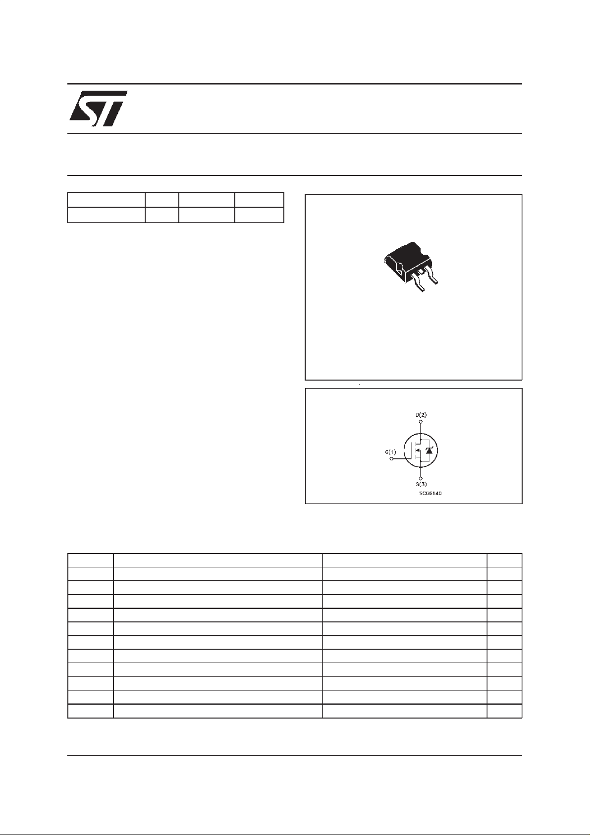
■ SURFACE-MOUNTINGD2PAK (TO-263)
POWERPACKAGEIN TAPE & REEL
(SUFFIX”T4”)
DESCRIPTION
This MOSFET series realized with STMicroelectronics unique STripFET process has specifically
been designed to minimize input capacitanceand
gate charge. It is therefore suitable as primary
switch in advanced high-efficiency, high-frequency isolated DC-DC converters for Telecom and
Computerapplications. It is also intended for any
applicationswith low gate drive requirements.
R
DS(on)
I
D
STB40NF10
PRELIMINARY DATA
3
1
D2PAK
TO-263
(Suffix”T4”)
INTERNAL SCHEMATIC DIAGRAM
APPLICATIONS
■ HIGH-EFFICIENCYDC-DC CONVERTERS
■ UPSAND MOTORCONTROL
ABSOLUTE MAXIMUM RATINGS
Symbol Parameter Value Uni t
V
V
V
I
DM
P
E
AS
T
(•) Pulse width limitedby safe operating area (1) starting Tj
Dra in- sour c e Volta ge (VGS= 0) 100 V
DS
Drain- gate Voltage (RGS=20kΩ) 100 V
DGR
Gate-s ource Voltage ± 20 V
GS
Dra in Cu rr ent (cont inuous) at Tc=25oC40A
I
D
Dra in Cu rr ent (cont inuous) at Tc= 100oC25A
I
D
(
Dra in Cu rr ent (pulsed) 160 A
•)
Tot al Dissipatio n at Tc=25oC 140 W
tot
Der ati ng F a c tor 0.93 W/
(1) Single Pu ls e Avalanche Ener gy 135 mJ
St orage T e m pe ra t ure -65 to 175
stg
Max. Operating Jun ct ion Te m pe rat ur e 175
T
j
=25oC,ID=40A , VDD= 50V
o
C
o
C
o
C
May 2000
1/6
STB40NF10
THERMAL DATA
R
thj-case
R
thj-amb
T
Ther mal Resistanc e Junct ion-case Max
Ther mal Resistanc e Junct ion-ambient Max
Maximum Lead Tempe ra t ure For Solder ing Purpose
l
1.07
62.5
300
o
C/W
o
C/W
o
C
ELECTRICAL CHARACTERISTICS
=25oC unless otherwisespecified)
(T
case
OFF
Symbol Parameter Test Conditions Min. Typ. Max. Unit
V
(BR)DSS
Drain-source
ID=250µAVGS= 0 100 V
Break dow n Voltage
I
DSS
I
GSS
Zero Gate Voltage
Drain Current (V
GS
Gat e- bod y Leak ag e
Current (V
DS
=0)
=0)
V
=MaxRating
DS
=MaxRating Tc=125oC
V
DS
V
= ± 20 V ± 100 nA
GS
1
10
ON(∗)
Symbol Parameter Test Conditions Min. Typ. Max. Unit
V
GS(th)
R
DS(on)
Gate Threshold Voltage VDS=VGSID= 250 µA22.84V
Sta t ic Drain-s ource On
VGS=10V ID= 20 A 0.030 0.035 Ω
Resistance
I
D(on)
On State Drain Current VDS>I
D(on)xRDS(on)max
40 A
VGS=10V
DYNAMIC
Symbol Parameter Test Conditions Min. Typ. Max. Unit
g
(∗)Forward
fs
Tr ansc on duc tance
C
C
C
Input Capaci t anc e
iss
Out put Capac it ance
oss
Reverse Transfer
rss
Capacit a nc e
VDS>I
D(on)xRDS(on)maxID
=20 A 20 S
VDS=25V f=1MHz VGS= 0 1800
270
110
µA
µ
pF
pF
pF
A
2/6
 Loading...