

SGS Thomson Microelectronics STB3NC60 Datasheet
STB3NC60
N - CHANNEL600V - 3.3Ω -3A-D2PAK/I2PAK
TYPE V
DSS
R
DS(on)
I
D
ST B3 NC60 600 V < 3 .6 Ω 3A
ν TYPICALR
ν EXTREMELY HIGHdv/dt CAPABILITY
ν 100% AVALANCHETESTED
ν VERY LOW INTRINSIC CAPACITANCES
ν GATECHARGE MINIMIZED
DS(on)
= 3.3 Ω
DESCRIPTION
The PowerMESHII is the evolution of the first
generation of MESH OVERLAY. The layout
refinements introduced greatly improve the
Ron*area figure of merit while keeping the device
at the leading edge for what concerns switching
speed, gatecharge and ruggedness.
APPLICATIONS
ν HIGH CURRENT, HIGH SPEEDSWITCHING
ν SWITCHMODEPOWER SUPPLIES (SMPS)
ν DC-ACCONVERTERSFOR WELDING
EQUIPMENTAND UNINTERRUPTIBLE
POWERSUPPLIESAND MOTORDRIVE
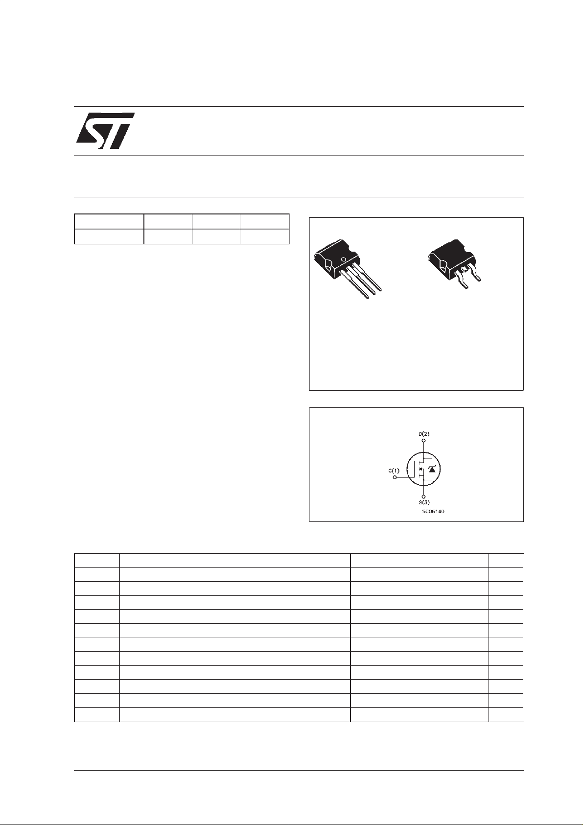
PowerMESH
3
2
1
I2PAK
TO-262
(Suffix”-1”)
ΙΙ MOSFET
D2PAK
TO-263
(Suffix ”T4”)
INTERNAL SCHEMATIC DIAGRAM
3
1
ABSOLUTE MAXIMUM RATINGS
Symbol Parameter Value Uni t
V
V
V
I
DM
P
dv/dt(
T
(•) Pulse width limited by safe operating area (1)ISD≤3A, di/dt ≤ 100 A/µs, VDD≤ V
February 2000
Drain-source Volt age (VGS= 0 ) 600 V
DS
Drain- gate Voltage ( RGS=20kΩ)
DGR
Gate-s ource Voltage ± 30 V
GS
Drain Current (c ont in uous ) at Tc=25oC3A
I
D
I
Drain Current (c ont in uous ) at Tc= 100oC 1.9 A
D
600 V
(•) Drain Current (p ulsed) 12 A
Tot al D issipation at Tc=25oC80W
tot
Derating Factor 0.64 W/
1) Peak Diode Rec overy voltage slope 4 V/ns
St orage T e m perature -65 to 150
stg
Max. O per ating J u nc tion Temperature 150
T
j
,Tj≤T
(BR)DSS
JMAX
o
C
o
C
o
C
1/9
STB3NC60
THERMAL DATA
R
thj-cas e
R
thj-amb
R
thc-sin k
T
AVALANCHE CHARACTERISTICS
Symb ol Parameter Max Value Uni t
I
AR
E
Therma l Resist ance Junct i on- case Max 1.56
Therma l Resist ance Junct i on- ambient Max
Therma l Resist ance Case-sink Typ
Maxim um Lead Tem pe ra t ure For Soldering P urpose
l
Avalanc h e Current , Repe t it ive or N ot-Repetitive
(pulse w idth limited b y T
Single P ulse A v alanche Energy
AS
(starting T
=25oC, ID=IAR,VDD=50V)
j
max)
j
62.5
0.5
300
3A
100 mJ
o
C/W
o
C/W
o
C/W
o
C
ELECTRICAL CHARACTERISTICS (T
=25oC unlessotherwisespecified)
case
OFF
Symb ol Parameter Test C o n ditions Mi n . Typ . Max. Unit
V
(BR) DSS
Drain-s ource
= 250 µAVGS=0
I
D
600 V
Break down Volt age
I
DSS
I
GSS
Zero Gate Voltage
Drain Cur rent (V
GS
Gate-body Leaka ge
Current (V
DS
=0)
=0)
V
=MaxRating
DS
= Max Rating Tc= 125oC
V
DS
= ± 30 V
V
GS
1
50
± 100 nA
ON (∗)
Symb ol Parameter Test C o n ditions Mi n . Typ . Max. Unit
V
GS(th)
R
DS(on)
Gate Th re sho ld Volt age
Static D rain-sourc e O n
V
DS=VGSID
=250µA
VGS= 10V ID= 1.5 A 3.3 3.6 Ω
234V
Resistance
I
D(on)
On State Drain Current VDS>I
D(on)xRDS(on)max
3A
VGS=10V
DYNAMIC
Symb ol Parameter Test C o n ditions Mi n . Typ . Max. Unit
g
(∗)Forward
fs
Transconduct ance
C
C
C
Input Capac itance
iss
Output Capacitance
oss
Reverse Transfer
rss
Capacit ance
VDS>I
D(on)xRDS(on)maxID
=1.5A 2 S
VDS=25V f=1MHz VGS= 0 400
57
7
µA
µA
pF
pF
pF
2/9
STB3NC60
ELECTRICAL CHARACTERISTICS (continued)
SWITCHING ON
Symb ol Parameter Test C o n ditions Mi n . Typ . Max. Unit
t
d(on)
t
r
Turn-on Time
Rise Time
VDD=300V ID=1.5A
=4.7 Ω VGS=10V
R
G
(see test circuit, figure 3)
Q
Q
Q
Total Gate Charge
g
Gate-Sourc e Char ge
gs
Gate-Drain Char g e
gd
VDD=480V ID=3A VGS=10V 13
SWITCHING OFF
Symb ol Parameter Test C o n ditions Mi n . Typ . Max. Unit
t
r(Voff)
t
Off -volt age Ris e Time
Fall Time
t
f
Cross -over Time
c
VDD=480V ID=3A
=4.7 Ω VGS=10V
R
G
(see test circuit, figure 5)
SOURCEDRAINDIODE
Symb ol Parameter Test C o n ditions Mi n . Typ . Max. Unit
I
SD
I
SDM
V
SD
t
Q
I
RRM
(∗) Pulsed: Pulse duration = 300µs, dutycycle 1.5 %
(•) Pulse width limited by safe operatingarea
Source-drain Current
(•)
Source-drain Current
(pulsed)
(∗)ForwardOnVoltage ISD=3A VGS=0 1.6 V
Revers e R ec overy
rr
Time
Revers e R ec overy
rr
= 3 A di/dt = 100 A/µs
I
SD
=100V Tj= 150oC
V
DD
(see test circuit, figure 5)
Charge
Revers e R ec overy
Current
9
13
18.2 nC
2.3
4.4
13
15
21
3
12
420
1.5
7.1
ns
ns
nC
nC
ns
ns
ns
A
A
ns
µC
A
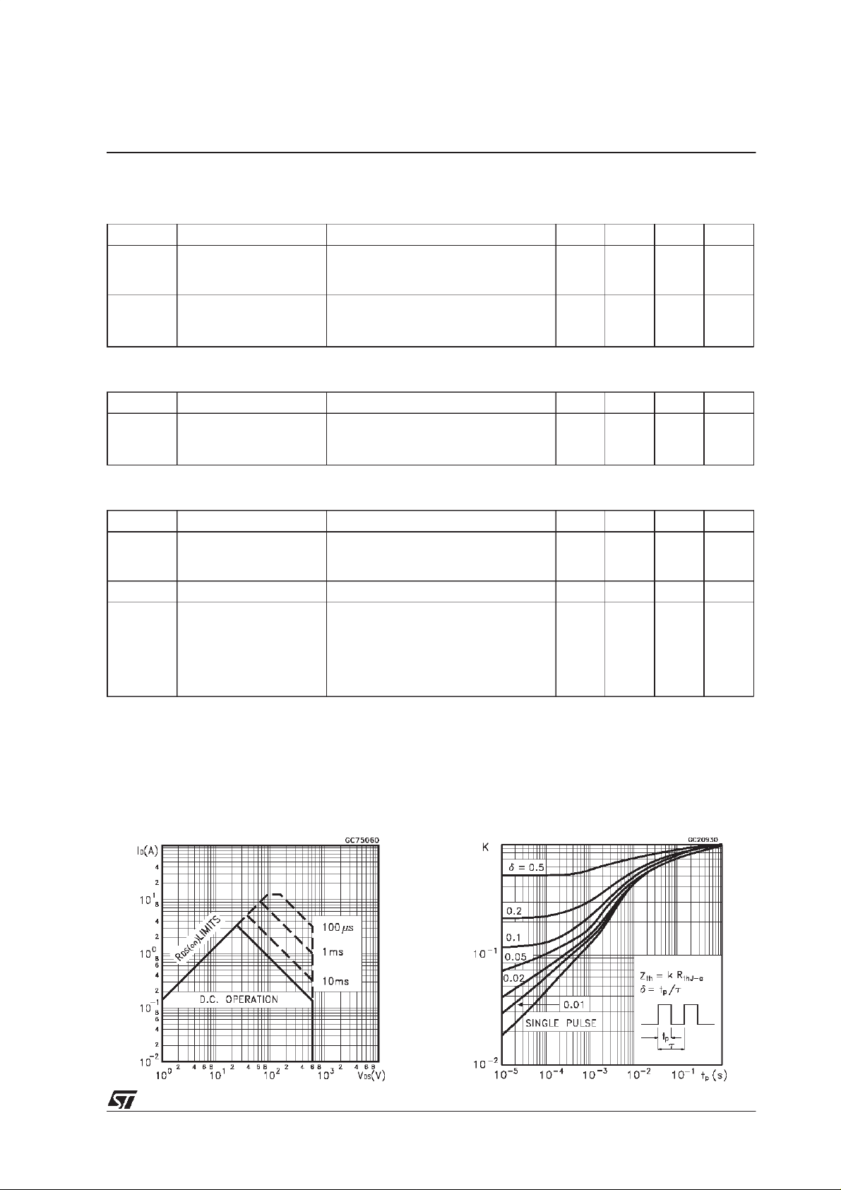
Safe Operating Area for D2PAK/I2PAK ThermalImpedanceforD2PAK/I2PAK
3/9
 Loading...