

SGS Thomson Microelectronics STB3NB60 Datasheet
STB3NB60
N - CHANNEL 600V - 3.3Ω - 3.3A - D2PAK/I2PAK
PowerMESH MOSFET
TYPE V
DSS
R
DS(on)
I
D
STB3NB60 600 V <3.6 Ω 3.3 A
■ TYPICALR
■ EXTREMELY HIGH dv/dt CAPABILITY
■ 100% AVALANCHETESTED
■ VERYLOW INTRINSIC CAPACITANCES
■ GATECHARGEMINIMIZED
DS(on)
=3.3 Ω
DESCRIPTION
Using the latest high voltage MESH OVERLAY
process, SGS-Thomson has designed an
advanced family of power MOSFETs with
outstanding performances. The new patent
pending strip layout coupled with the Company’s
proprietary edge termination structure, gives the
lowest RDS(on) per area, exceptional avalanche
and dv/dt capabilities and unrivalled gate charge
and switching characteristics.
APPLICATIONS
■ HIGH CURRENT, HIGH SPEEDSWITCHING
■ SWITCHMODEPOWER SUPPLIES(SMPS)
■ DC-ACCONVERTERS FOR WELDING
EQUIPMENTAND UNINTERRUPTIBLE
POWERSUPPLIESAND MOTORDRIVE
3
1
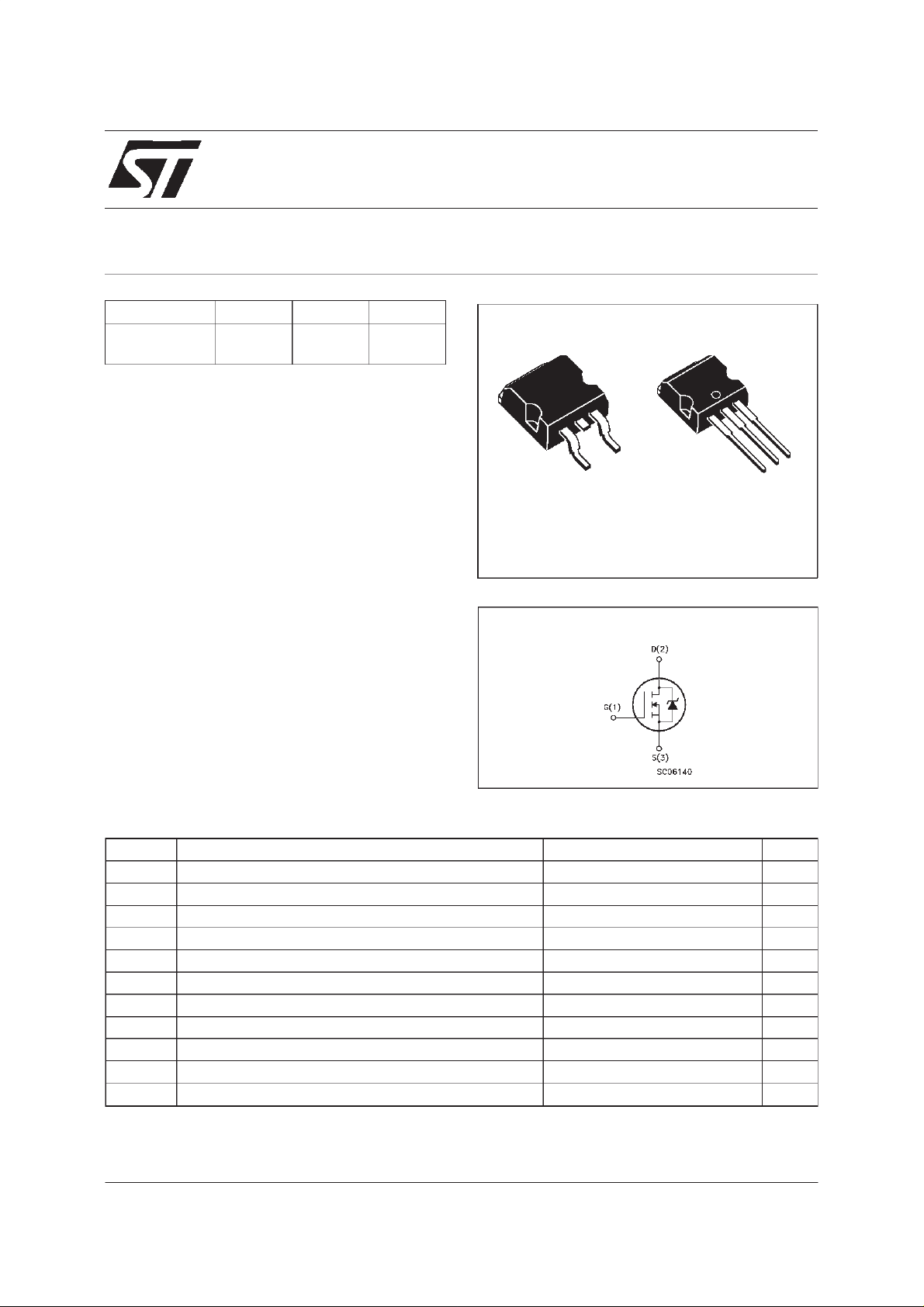
D2PAK
TO-263
(Suffix ”T4”)
INTERNAL SCHEMATIC DIAGRAM
(Suffix ”-1”)
1
I2PAK
TO-262
3
2
ABSOLUTE MAXIMUM RATINGS
Symb o l Para meter Value Uni t
V
V
V
I
DM
P
dv/dt(
T
(•) Pulse width limited by safe operating area (1)ISD≤3.3A, di/dt ≤ 200 A/µs, VDD≤ V
June 1998
Drain-source Voltage (VGS=0) 600 V
DS
Drain- gate Voltage ( RGS=20kΩ)
DGR
Gat e- source Vo lt age ± 30 V
GS
I
Drain Cur rent ( continuous) at Tc=25oC3.3A
D
I
Drain Cur rent ( continuous) at Tc=100oC2.1A
D
600 V
(•) Dra in C urr ent (pulsed) 13.2 A
Tot al Dissipation at Tc=25oC80W
tot
Derating Factor 0.64 W/
1) Peak Diode Rec overy volt age s l ope 4.5 V/ns
Sto rage Tempe rature -65 to 150
stg
T
Max. Operating Ju nc t io n Tem peratur e 150
j
,Tj≤T
(BR)DSS
JMAX
o
C
o
C
o
C
1/9
STB3NB60
THERMAL DATA
R
thj-case
R
thj-amb
R
thc-sin k
T
AVALANCHE CHARACTERISTICS
Symbol Para met e r Max Value Uni t
I
AR
E
Ther mal Resist ance Junctio n-c a se Max 1.56
Ther mal Resist ance Junctio n-ambient Max
Ther mal Resist ance Case-sink T yp
Maximum Lead Temperat u re F o r Soldering Purp ose
l
Avalanche Cur rent, Rep etit ive or Not-Re petitive
(pulse width limited by T
Single Pulse Avalanche Energy
AS
(starting T
=25oC, ID=IAR,VDD=50V)
j
max)
j
62.5
0.5
300
3.3 A
100 mJ
o
C/W
o
C/W
o
C/W
o
C
ELECTRICAL CHARACTERISTICS (T
=25oC unlessotherwise specified)
case
OFF
Symbol Parameter Test Cond itions Min. Typ. M ax. Unit
V
(BR)DSS
Drain-sourc e
=250µAVGS=0
I
D
600 V
Breakdown V oltage
I
DSS
I
GSS
Zer o Gat e V o lt age
Drain Current (V
GS
Gat e-body Leaka ge
Current (V
DS
=0)
=0)
V
=MaxRating
DS
=MaxRating Tc=125oC
V
DS
= ± 30 V
V
GS
1
50
± 100 nA
ON (∗)
Symbol Parameter Test Cond itions Min. Typ. M ax. Unit
V
GS(th )
Gate Threshold
V
DS=VGSID
=250µA
345V
Voltage
R
DS(on)
Stati c D rain-source On
VGS=10V ID= 1.6 A 3.3 3.6 Ω
Resistance
I
D(on)
On State Drain Curre nt VDS>I
D(on)xRDS(on)max
3.3 A
VGS=10V
DYNAMIC
Symbol Parameter Test Cond itions Min. Typ. M ax. Unit
g
(∗)Forward
fs
Tr ansconductanc e
C
C
C
Input Capac i t an c e
iss
Out put C apa c itance
oss
Reverse Transf er
rss
Capa cit an c e
VDS>I
D(on)xRDS(on)maxID
=1.6A 1.2 2 S
VDS=25V f=1MHz VGS= 0 400
57
7
520
77
9
µA
µA
pF
pF
pF
2/9
STB3NB60
ELECTRICAL CHARACTERISTICS (continued)
SWITCHINGON
Symbol Parameter Test Cond itions Min. Typ. M ax. Unit
t
d(on)
Turn-on Time
r
Rise Time
t
VDD=300V ID=1.6A
=4.7 Ω VGS=10V
R
G
11
7
(see test circuit, figure 3)
Q
Q
Q
Total Gate Charge
g
Gat e-Sour ce Cha rge
gs
Gate-Drain Charge
gd
VDD=480V ID=3.3A VGS=10V 15
6.2
5.6
SWITCHINGOFF
Symbol Parameter Test Cond itions Min. Typ. M ax. Unit
t
r(Voff)
t
t
Of f - voltage Rise Time
Fall Time
f
Cross-ov er Time
c
VDD=480V ID=3.3A
=4.7 Ω VGS=10V
R
G
(see test circuit, figure 5)
11
13
18
SOURCE DRAIN DIODE
Symbol Parameter Test Cond itions Min. Typ. M ax. Unit
I
SD
I
SDM
V
SD
t
Q
I
RRM
(∗) Pulsed: Pulse duration =300 µs, duty cycle1.5 %
(•) Pulse width limited by safe operating area
Source-drain Curre nt
(•)
Source-drain Curre nt
(pulsed)
(∗) For ward On Vo ltage ISD=3.3A VGS=0 1.6 V
Reverse Recov er y
rr
Time
Reverse Recov er y
rr
= 3.3 A di/dt = 100 A /µs
I
SD
=100V Tj=150oC
V
DD
(see test circuit, figure 5)
500
2.1
Charge
Reverse Recov er y
8.5
Current
17
11
22 nC
16
18
25
3.3
13.2
ns
ns
nC
nC
ns
ns
ns
A
A
ns
µC
A
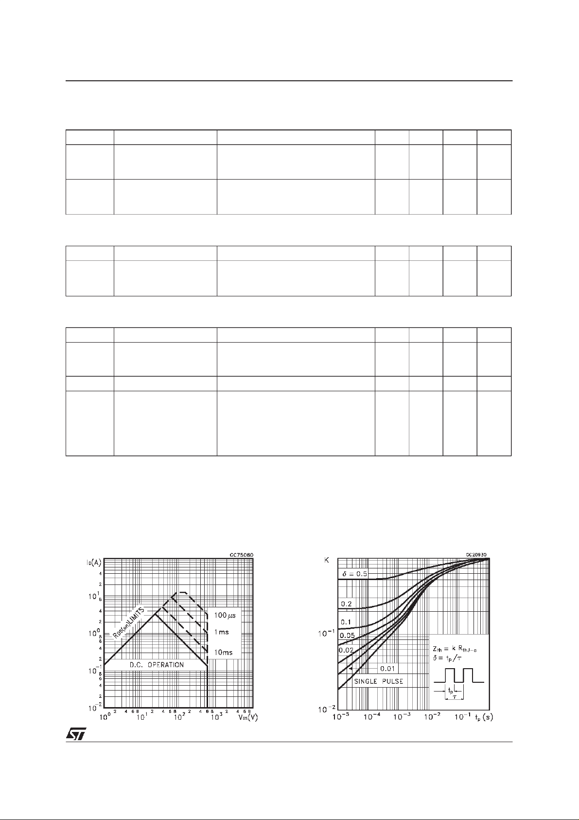
Safe Operating Areafor D2PAK/I2PAK ThermalImpedance for D2PAK/I2PAK
3/9
 Loading...