

N - CHANNEL 100V - 0.07Ω - 24A TO-263
LOW GATE CHARGE STripFET POWER MOSFET
TYPE V
DSS
ST B24NF10 100 V < 0.0 77 Ω 24 A
■ TYPICALR
■ EXCEPTIONALdv/dtCAPABILITY
■ 100%AVALANCHETESTED
■ SURFACE-MOUNTINGD
DS(on)
= 0.07 Ω
POWERPACKAGEIN TAPE & REEL
(SUFFIX”T4”)
DESCRIPTION
This MOSFET series realized with
STMicroelectronicsunique STripFET process has
specifically been designed to minimize input
capacitance and gate charge. It is therefore
suitable as primary switch in advanced
high-efficiency, high-frequency isolated DC-DC
converters for Telecom and Computer
applications. It is also intended for any
applicationswith low gate drive requirements.
R
DS(on)
2
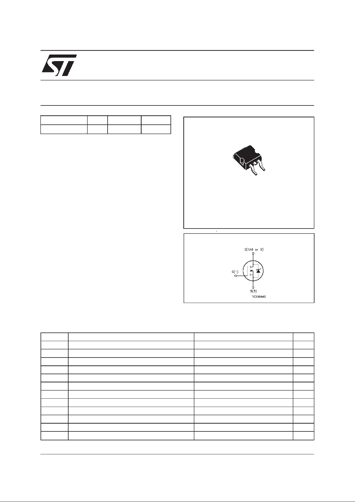
PAK(TO-263)
I
D
STB24NF10
PRELIMINARY DATA
3
1
D2PAK
TO-263
(Suffix ”T4”)
INTERNAL SCHEMATIC DIAGRAM
APPLICATIONS
■ HIGH-EFFICIENCYDC-DC CONVERTERS
■ UPSAND MOTORCONTROL
ABSOLUTE MAXIMUM RATINGS
Symbol Parameter Value Uni t
V
V
V
I
DM
P
dv/ dt (
E
AS
T
(•) Pulse width limitedby safe operating area (2) starting Tj
April 2000
Dra in- sour c e Vol ta ge (VGS= 0) 100 V
DS
Drain- gate Voltage (RGS=20kΩ) 100 V
DGR
Gate-s ource Voltage ± 20 V
GS
Dra in Current ( cont inuous) at Tc=25oC24A
I
D
Dra in Current ( cont inuous) at Tc= 100oC15A
I
D
(•) Dra in Current ( pulsed) 96 A
Tot al Dissipatio n a t Tc=25oC80W
tot
Der ati ng Fact or 0.53 W/
1 ) Peak Diode Reco ve ry volta ge slope 9 V/ns
(2) Single Pu lse Avalanche Energy 75 m J
St orage T e m pe ra tur e -65 to 175
stg
Max. Operat ing Junct ion Temperat ur e 175
T
j
=25oC, ID=24A, VDD= 50V (1) ISD≤ 24 A, di/dt ≤ 300A/µs, VDD≤ V
(BR)DSS,Tj≤TJMA
o
C
o
C
o
C
1/6
STB24NF10
THERMAL DATA
R
thj-case
R
thj-amb
T
Ther mal Resistanc e Junct ion-case Max
Ther mal Resistanc e Junct ion-ambient Max
Maximum Lead Temperat ur e For So lder ing Purp ose
l
1.87
62.5
300
o
C/W
o
C/W
o
C
ELECTRICAL CHARACTERISTICS
=25oC unless otherwisespecified)
(T
case
OFF
Symbol Parameter Test Conditions Min. Typ. Max. Unit
V
(BR)DSS
Drain-source
ID=250µAVGS= 0 100 V
Break dow n Voltage
I
DSS
I
GSS
Zero Gate Voltage
Drain Current ( V
GS
Gat e- bod y L eak ag e
Current (V
DS
=0)
=0)
V
=MaxRating
DS
=MaxRating Tc=125oC
V
DS
V
= ± 20 V ± 100 nA
GS
1
10
ON(∗)
Symbol Parameter Test Conditions Min. Typ. Max. Unit
V
GS(th)
R
DS(on)
Gate Threshold Voltage VDS=VGSID= 250 µ A 234V
Sta t ic Drain-sourc e On
VGS=10V ID= 12 A 0.07 0. 07 7 Ω
Resistance
I
D(on)
On State Drain Current VDS>I
D(on)xRDS(on)max
24 A
VGS=10V
DYNAMIC
Symbol Parameter Test Conditions Min. Typ. Max. Unit
g
(∗)Forward
fs
Tr ansc on duc tance
C
C
C
Input C apacitance
iss
Out put Capacitance
oss
Reverse Tr ansfer
rss
Capacit a nc e
VDS>I
D(on)xRDS(on)maxID
=12 A 20 S
VDS=25V f=1MHz VGS= 0 870
125
52
µA
µ
pF
pF
pF
A
2/6
 Loading...