

SGS Thomson Microelectronics STB20NM50FD Datasheet
STB20NM50FD
N-CHANNEL 500V - 0.20Ω - 20A D2PAK
FDmesh™Power MOSFET (With FAST DIODE)
PRELIMINARY DATA
TYPE V
STB20NM50FD 500V < 0.25Ω 20 A
n
TYPICAL RDS(on) = 0.20Ω
n
HIGH dv/dt AND AVALANCHE CAPABILITIES
n
100% AVALANCHE TESTED
n
LOW INPUT CAPACITANCE AND GATE
DSS
R
DS(on)
I
D
CHARGE
n
LOW GATE INPUT RESIST ANC E
n
TIGHT PROCESS CONTROL AND HIGH
MANUFACTURING YIELDS
DESCRIPTION
The FDmesh™
associates all advantages of re-
duced on-resistance and fast swi tching with an intrinsic fast-recovery body diode. It is therefore
strongly recommended for bridge topologies, in particular ZVS phase-shift converters.
APPLICATIONS
n
ZVS PHASE-SHIFT FULL BRIDGE
CONVERTERS FOR SMPS AND WELDING
EQUIPMENT
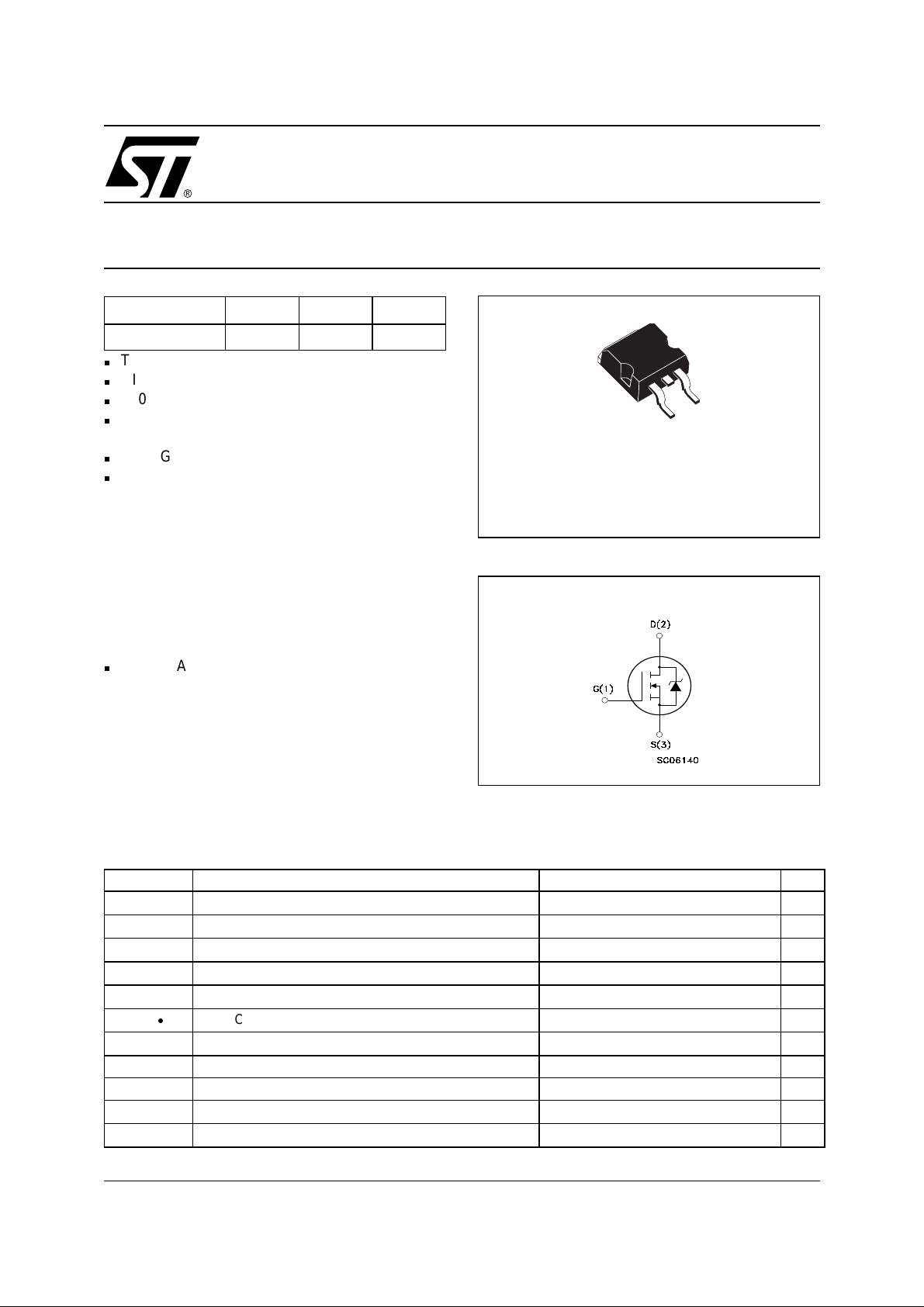
3
1
D2PAK
INTERNAL SCHEMATIC DIAGRAM
ABSOLUTE MAXIMUM RATINGS
Symbol Parameter Value Unit
V
DS
V
DGR
V
GS
I
D
I
D
I
DM
P
TOT
dv/dt Peak Diode Recovery voltage slope 6 V/ns
T
stg
T
j
(•)Pu l se width limited by safe operating area
November 2001
Drain-source Voltage (VGS = 0)
Drain-gate Voltage (RGS = 20 kΩ)
Gate- source Voltage ±30 V
Drain Current (continuos) at TC = 25°C
Drain Current (continuos) at TC = 100°C
(l)
Drain Current (pulsed) 80 A
Total Dissipation at TC = 25°C
Derating Factor 0.88 W/°C
Storage Temperature –65 to 150 °C
Max. Operating Junction Temperature 150 °C
500 V
500 V
20 A
14 A
192 W
1/7

STB20NM50FD
THERMA L D ATA
Rthj-case Thermal Resistance Junction-case Max 0.65 °C/W
Rthj-amb Thermal Resistance Junction-ambient Max 62.5 °C/W
T
l
AVALANCHE CHARACTERISTICS
Symbol Parameter Max Value Unit
I
AR
E
AS
ELECTRICAL CHARACTERISTICS (TCASE = 25 °C UNLESS OTHERWISE SPECIFIED)
OFF
Symbol Parameter Test Conditions Min. Typ. Max. Unit
V
(BR)DSS
I
DSS
I
GSS
Maximum Lead Temperature For Soldering Purpose 300 °C
Avalanche Current, Repetitive or Not-Repetitive
(pulse width limited by T
max)
j
Single Pulse Avalanche Energy
(starting T
Drain-source
= 25 °C, ID = IAR, VDD = 35 V)
j
ID = 250 µA, VGS = 0 500 V
10 A
700 mJ
Breakdown Voltage
Zero Gate Voltage
Drain Current (V
GS
Gate-body Leakage
Current (V
DS
= 0)
= 0)
V
= Max Rating
DS
V
= Max Rating, TC = 125 °C
DS
V
= ±30V ±100 nA
GS
1µA
100 µA
ON
(1)
Symbol Parameter Test Conditions Min. Typ. Max. Unit
V
GS(th)
R
DS(on)
Gate Threshold Voltage
Static Drain-source On
V
= VGS, ID = 250µA
DS
VGS = 10V, ID = 10A
345V
0.20 0.25 Ω
Resistance
DYNAMIC
Symbol Parameter Test Conditions Min. Typ. Max. Unit
(1) Forward Transconductance VDS > I
g
fs
C
iss
C
oss
C
rss
C
oss eq.
Input Capacitance
Output Capacitance 285 pF
Reverse Transfer
Capacitance
(2) Equivalent Output
Capacitance
R
G
1. Pulsed: Pu l se duration = 300 µs, duty c yc l e 1.5 %.
2. C
Gate Input Resistance f=1 MHz Gate DC Bias = 0
is defined as a constant equivalent capacitance giving the same charging time as C
oss eq.
V
.
DSS
I
= 10A
D
V
DS
VGS = 0V, VDS = 0V to 400V 130 pF
Test Signal Level = 20mV
Open Drain
D(on)
x R
DS(on)max,
= 25V, f = 1 MHz, VGS = 0
9S
1480 pF
34 pF
1.7 Ω
when VDS increase s fr om 0 to 80%
oss
2/7

STB20NM50FD
ELECTRICAL CHARACTERISTICS (CONTINUED)
SWITCHING ON
Symbol Parameter Test Conditions Min. Typ. Max. Unit
V
t
d(on)
Q
Q
Q
t
r
g
gs
gd
Turn-on Delay Time
Rise Time 16 ns
Total Gate Charge
Gate-Source Charge 13 nC
Gate-Drain Charge 19 nC
SWITCHING OFF
Symbol Param eter Test Conditions Min. Typ. Max. Unit
t
r(Voff)
t
f
t
c
Off-voltage Rise Time
Fall Time 8.5 ns
Cross-over Time 23 ns
SOURCE DRAIN DIODE
Symbol Parameter Test Conditions Min. Typ. Max. Unit
I
SD
I
SDM
VSD (1)
t
rr
Q
rr
I
RRM
Note: 1. Pulsed: Pulse duration = 300 µs, duty cycle 1.5 %.
2. Pulse width lim i t ed by safe ope rat i ng area.
(2)
Source-drain Current 20 A
Source-drain Current (pulsed) 80 A
Forward On Voltage
Reverse Recovery Time
Reverse Recovery Charg e 1.6 µC
Reverse Recovery Curren t 15 A
= 250V, ID = 10A
DD
RG= 4.7Ω VGS = 10V
(see test circuit, Figure 3)
V
= 400V, ID = 20A,
DD
V
= 10V
GS
V
= 400V, ID = 20A,
DD
RG= 4.7Ω, V
GS
= 10V
(see test circuit, Figure 5)
ISD = 20A, VGS = 0
I
= 20A, di/dt = 100A/µs,
SD
V
= 50V
DD
(see test circuit, Figure 5)
24 ns
40 56 nC
9ns
1.5 V
220 ns
3/7
 Loading...