

SGS Thomson Microelectronics STB19NB20-1 Datasheet
STP19NB20 - STP19NB20FP
STB19NB20-1
N-CHANNEL 200V - 0.15Ω - 19A - TO-220/TO-220FP/I2PAK
PowerMESH™ MOSFET
TYPE V
STP19NB20
STP19NB20 FP
STB19NB20 -1
■ TYPICAL R
■ EXTREMELY HIGH dv/d t C APABILITY
■ 100% AVALANCHE TESTED
■ NEW HIGH VOLTAGE BENCHMARK
■ GATE CHARGE MINIMIZED
DS
DSS
200 V
200 V
200 V
(on) = 0.15 Ω
R
DS(on)
< 0.18 Ω
< 0.18 Ω
< 0.18 Ω
I
D
19 A
10 A
19 A
DESCRIPTION
Using the latest high voltage MESH OVERLAY™
process, STMicroelectronics has designed an advanced family of power MOSFETs with outstanding
performances. The new patent pending strip layout
coupled with the Company’s proprieraty edge termination structure, gives the lowest RDS(on) per area,
exceptional avalanche and dv/dt capabilities and
unrivalled gate charge and switching characteristics.
APPLICATIONS
■ HIGH CURRENT, HIGH SPEED SWITCHING
■ SWITH MODE POWER SUPPLIES ( SMPS)
■ DC-AC CONVERTERS FOR TELECOM,
INDUSTRIAL AND CONSUMER
ENVIRONMENT
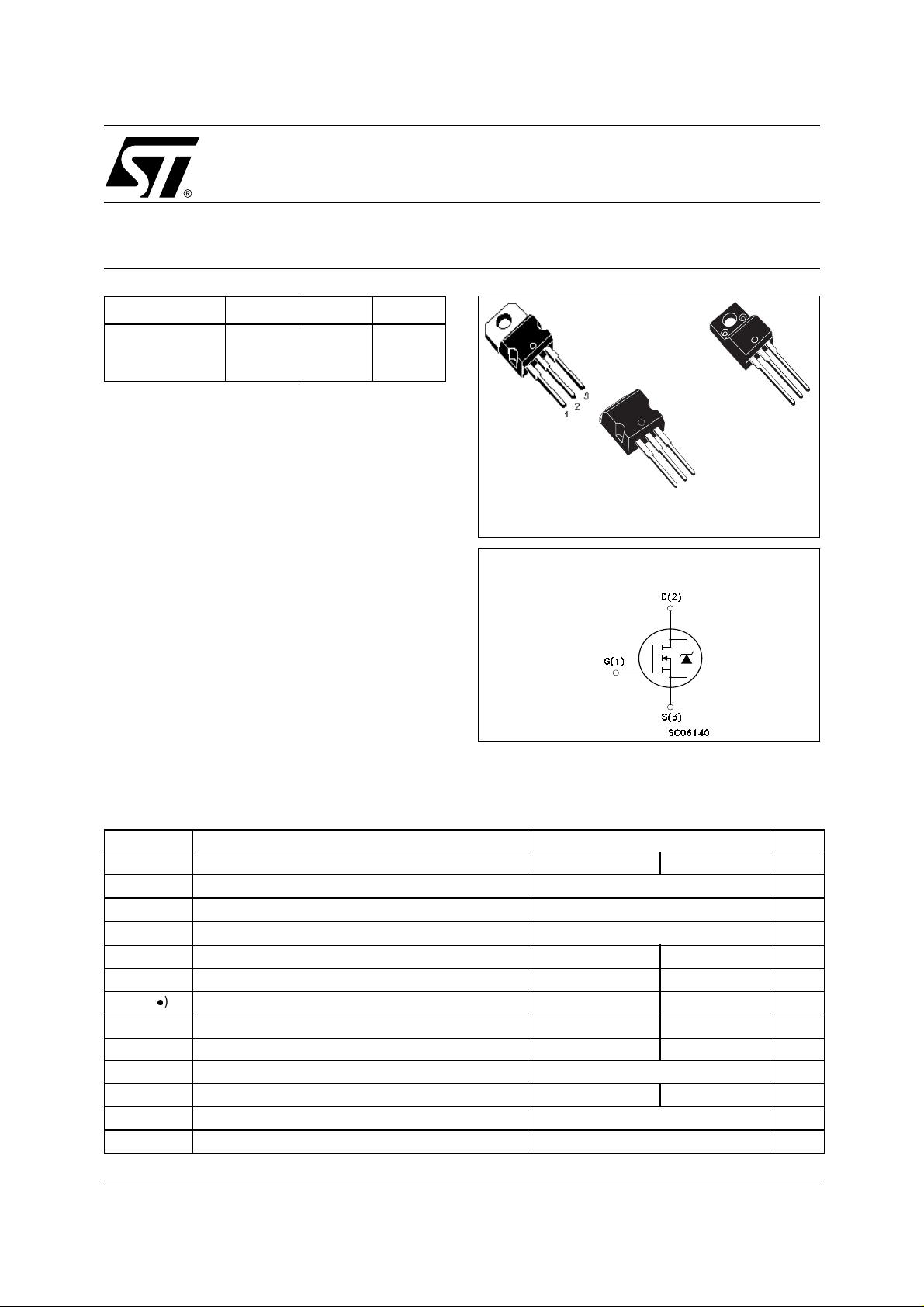
TO-220
3
2
1
I2PAK
(Tabless TO-220)
INTERNAL SCHEMATIC DIAGRAM
TO-220FP
1
3
2
ABSOLUTE MAXIMUM RATINGS
Symbol Parameter Value Unit
STP(B)19NB20(-1) STP19NB20FP
V
DS
V
DGR
V
GS
I
D
I
D
I
DM
P
TOT
dv/dt (1) Peak Diode Recovery voltage slope 5.5 V/ns
V
ISO
T
stg
T
(•)Pu l se width limite d by safe operating area
Drain-source Voltage (VGS = 0)
Drain-gate Voltage (RGS = 20 kΩ)
200 V
200 V
Gate- source Voltage ± 30 V
Drain Current (continuous) at TC = 25°C
Drain Current (continuous) at TC = 100°C
(l)
Drain Current (pulsed) 76 76 A
Total Dissipation at TC = 25°C
19 10 A
12 6.0 A
125 35 W
Derating Factor 1 0.28 W/°C
Insulation Withstand Voltage (DC) - 2500 V
Storage Temperature –65 to 150 °C
Max. Operating Junction Temperature 150 °C
j
(1)ISD ≤19 A, di/dt ≤300A/µs, VDD ≤ V
(BR)DSS
, Tj ≤ T
JMAX
1/12August 2002
STP19NB20/FP/STB19NB20-1
THERMA L D ATA
TO-220/I2PAK
Rthj-case Thermal Resistance Junction-case Max 1 3.57 °C/W
Rthj-amb Thermal Resistance Junction-ambient Max 62.5 °C/W
T
l
Maximum Lead Temperature For Soldering Purpose 300 °C
AVALANCHE CHARACTERISTICS
Symbol Parameter Max Value Unit
I
AR
E
AS
Avalanche Current, Repetitive or Not-Repetitive
(pulse width limited by T
max)
j
Single Pulse Avalanche Energy
(starting T
= 25 °C, ID = IAR, VDD = 50 V)
j
ELECTRICAL CHARACTERISTICS (TCASE = 25 °C UNLESS OTHERWISE SPECIFIED)
OFF
Symbol Parameter Test Conditions Min. Typ. Max. Unit
V
(BR)DSS
I
DSS
I
GSS
Drain-source
Breakdown Voltage
Zero Gate Voltage
Drain Current (V
GS
Gate-body Leakage
Current (V
DS
= 0)
= 0)
ID = 250 µA, VGS = 0 200 V
= Max Rating
V
DS
V
= Max Rating, TC = 125 °C
DS
V
= ±30V ±100 nA
GS
TO-220FP
19 A
580 mJ
1µA
10 µA
ON
(1)
Symbol Parameter Test Conditions Min. Typ. Max. Unit
V
V
GS(th)
R
DS(on)
Gate Threshold Voltage
Static Drain-source On
= VGS, ID = 250µA
DS
VGS = 10V, ID = 9.5 A
345V
0.15 0.18 Ω
Resistance
DYNAMIC
Symbol Parameter Test Conditions Min. Typ. Max. Unit
(1) Forward Transconductance VDS > I
g
fs
C
iss
C
oss
C
rss
Input Capacitance
Output Capacitance 285 pF
Reverse Transfer
Capacitance
ID= 9.5 A
V
DS
D(on)
x R
DS(on)max,
= 25V, f = 1 MHz, VGS = 0
3S
1000 pF
45 pF
2/12
STP19NB20/FP/STB19N B20-1
ELECTRICAL CHARACTERISTICS (CONTINUED)
SWITCHING ON
Symbol Parameter Test Conditions Min. Typ. Max. Unit
V
t
d(on)
Q
Q
Q
t
r
g
gs
gd
Turn-on Delay Time
Rise Time 15 ns
Total Gate Charge
Gate-Source Charge 9.5 nC
Gate-Drain Charge 13 nC
SWITCHING OFF
Symbol Parameter Test Conditions Min. Typ. Max. Unit
t
r(Voff)
t
f
t
c
Off-voltage Rise Time
Fall Time 10 ns
Cross-over Time 20 ns
SOURCE DRAIN DIODE
Symbol Parameter Test Conditions Min. Typ. Max. Unit
I
SD
I
SDM
VSD (1)
t
rr
Q
rr
I
RRM
Note: 1. Pulsed: Puls e duration = 300 µs, duty cycle 1.5 %.
2. Pulse width limited by safe operating area.
Source-drain Current 19 A
(2)
Source-drain Current (pulsed) 76 A
Forward On Voltage
Reverse Recovery Time
Reverse Recovery Charge 1.5 µC
Reverse Recovery Current 14.5 A
= 100V, ID = 9.5 A
DD
RG=4.7Ω VGS = 10V
(see test circuit, Figure 3)
V
= 160V, ID = 19 A,
DD
V
= 10V
GS
V
= 160V, ID = 19 A,
DD
R
= 4.7Ω, V
G
GS
= 10V
(see test circuit, Figure 5)
ISD = 19 A, VGS = 0
I
= 19 A, di/dt = 100A/µs,
SD
V
= 50V, Tj = 150°C
DD
(see test circuit, Figure 5)
15 ns
29 40 nC
10 ns
1.5 V
210 ns
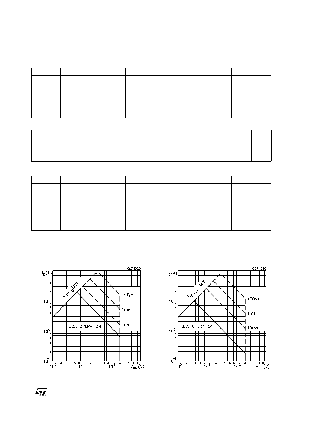
Safe Operating Area for TO-220FPSafe Operating Area for TO-220/I2PAK
3/12
STP19NB20/FP/STB19NB20-1
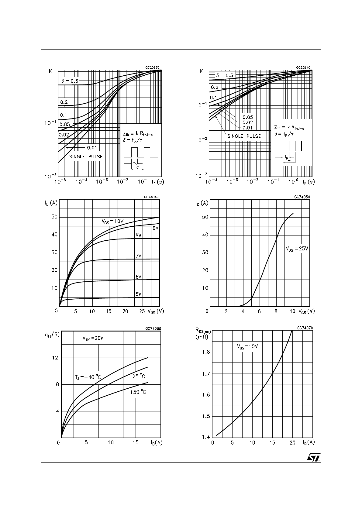
Thermal Impedance for TO-220/I
2
PAK Thermal Impedance for TO-220FP
Output Characteristics
Tranconductance
Tranfer Characteristics
Static Drain-Source On Resistance
4/12
 Loading...