

SGS Thomson Microelectronics STB16NS25 Datasheet
STB16NS25
N-CHANNEL 250V - 0.23Ω -16AD2PAK
MESH OVERLAY™ MOSFET
TYPE V
DSS
R
DS(on)
I
D
STB16NS25 250 V < 0.28 Ω 16 A
■ TYPICAL R
■ EXTREMELY HIGHdv/dt CAPABILITY
■ 100% AVALANCHE TESTED
(on) = 0.23 Ω
DS
DESCRIPTION
Using the latest high voltage MESH OVERLAY™
process, STMicroelectronics has designed an a dvanced family of power MOSFETs with outstanding
performance. The new patented STrip layout co upled with t he C ompany’s proprietary edge te rmin ation structure, makes it s uitable in coverters for
lighting applications.
APPLICATIONS
■ HIGH CURRENT, HIGH SPEED SWITCHING
■ SWITH MODE POWER SUPPLIES (SMPS)
■ DC-DC CONVERTERS FOR TELECOM,
INDUSTRIAL, AND LIGHTING EQUIPMENT
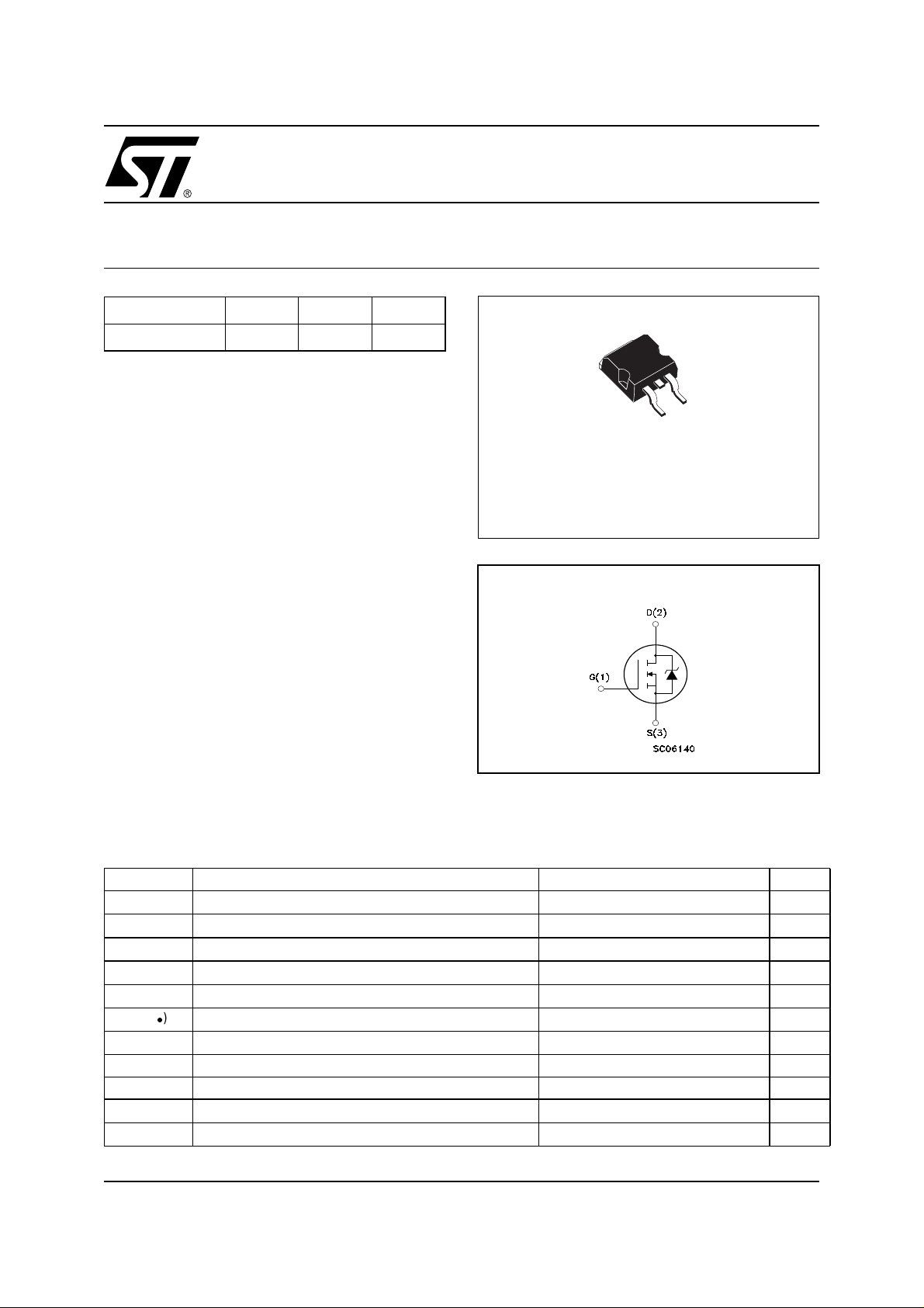
3
1
D2PAK
INTERNAL SCHEMATIC DIAGRAM
ABSOLUTE MAXIMUM RATINGS
Symbol Parameter Value Unit
V
DS
V
DGR
V
GS
I
D
I
D
IDM()
P
TOT
dv/dt (1) Peak Diode Recovery voltage slope 5 V/ns
T
stg
T
j
(•)Pulse width limited by safe operating area
Drain-source Voltage (VGS=0)
Drain-gate Voltage (RGS=20kΩ)
250 V
250 V
Gate- source Voltage ± 20 V
Drain Current (continuos) at TC= 25°C
Drain Current (continuos) at TC= 100°C
16 A
11 A
Drain Current (pulsed) 64 A
Total Dissipation at TC= 25°C
140 W
Derating Factor 1 W/°C
Storage Temperature –65 to 175 °C
Max. Operating Junction Temperature 175 °C
(1) ISD≤ 16A, di/dt≤300 A/µs, VDD≤ V
(BR)DSS
,Tj≤T
jMAX
1/9February 2003
STB16NS25
THERMAL DATA
Rthj-case Thermal Resistance Junction-case Max 0.9 °C/W
Rthj-amb Thermal Resistance Junction-ambient Max 62.5 °C/W
T
l
AVALANCHE CHARACTERISTICS
Symbol Parameter Max Value Unit
I
AR
E
AS
ELECTRICAL CHARACTERISTICS (TCASE = 25 °C UNLESS OTHERWISE SPECIFIED)
OFF
Symbol Parameter Test Conditions Min. Typ. Max. Unit
V
(BR)DSS
I
DSS
I
GSS
Maximum Lead Temperature For Soldering Purpose 300 °C
Avalanche Current, Repetitive or Not-Repetitive
(pulse width limited by T
max)
j
Single Pulse Avalanche Energy
(starting T
Drain-source
= 25 °C, ID=IAR,VDD=28V)
j
ID= 250 µA, VGS= 0 250 V
16 A
200 mJ
Breakdown Voltage
= Max Rating
Zero Gate Voltage
Drain Current (V
GS
Gate-body Leakage
Current (V
DS
=0)
=0)
V
DS
= Max Rating, TC= 125 °C
V
DS
V
= ± 20 V ±100 nA
GS
1µA
50 µA
ON (1)
Symbol Parameter Test Conditions Min. Typ. Max. Unit
V
GS(th)
R
DS(on)
Gate Threshold Voltage
Static Drain-source On
V
DS=VGS,ID
VGS=10V,ID=8A
= 250µA
234V
0.23 0.28 Ω
Resistance
DYNAMIC
Symbol Parameter Test Conditions Min. Typ. Max. Unit
(1) Forward Transconductance VDS>I
g
fs
C
iss
C
oss
C
rss
Input Capacitance
Output Capacitance 190 pF
Reverse Transfer
Capacitance
D(on)xRDS(on)max,
ID=8A
V
=25V,f=1MHz,VGS=0
DS
14 15 S
1270 pF
75 pF
2/9
STB16NS25
ELECTRICAL CHARACTERISTICS (CONTINUED)
SWITCHING ON
Symbol Parameter Test Conditions Min. Typ. Max. Unit
V
t
d(on)
Q
Q
Q
t
r
g
gs
gd
Turn-on Delay Time
Rise Time 25 ns
Total Gate Charge
Gate-Source Charge 8 nC
Gate-Drain Charge 22 nC
SWITCHING OFF
Symbol Parameter Test Conditions Min. Typ. Max. Unit
t
d(off)
t
t
r(Voff)
t
t
f
f
c
Turn-off- Delay Time
Fall Time
Off-voltage Rise Time
Fall Time
Cross-over Time
SOURCE DRAIN DIODE
Symbol Parameter Test Conditions Min. Typ. Max. Unit
I
SD
I
SDM
V
SD
t
rr
Q
rr
I
RRM
Note: 1. Pulsed: Pulse duration = 300 µs, duty cycle 1.5 %.
2. Pulse width limited by s afe operating area.
Source-drain Current 16 A
(2)
Source-drain Current (pulsed) 64 A
(1)
Forward On Voltage
Reverse Recovery Time
Reverse Recovery Charge 1.5 µC
Reverse Recovery Current 11.5 A
=125V,ID=8A
DD
R
= 4.7Ω VGS=10V
G
(see test circuit, Figure 3)
V
=200V,ID=16A,
DD
=10V
V
GS
VDD= 125V, ID=8A,
RG=4.7Ω, VGS= 10V
(see test circuit, Figure 3)
= 200V, ID=16A,
V
clamp
RG=4.7Ω, VGS= 10V
(see test circuit, Figure 5)
ISD=16A,VGS=0
I
= 16 A, di/dt = 100A/µs
SD
V
=33V,Tj= 150°C
DD
(see test circuit, Figure 5)
15 ns
60 80 nC
75
35
25
30
55
1.5 V
270 ns
ns
ns
ns
ns
ns
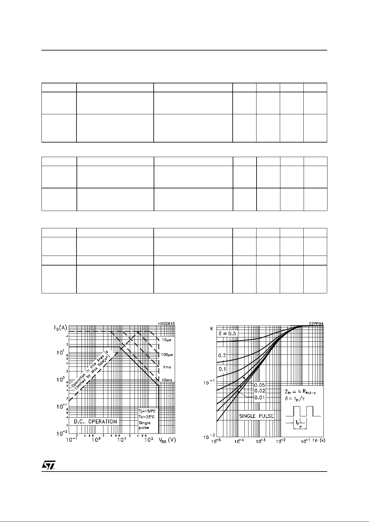
Thermal ImpedanceSafe Operati ng Area
3/9
 Loading...