

SGS Thomson Microelectronics STB16NB25 Datasheet
STB16NB25
N - CHANNEL 250V - 0.220Ω - 16A - TO-263
PowerMESH MOSFET
TYPE V
DSS
R
DS(on)
I
D
ST B16NB25 250 V < 0.28 Ω 16 A
■ TYPICALR
■ 100%AVALANCHETESTED
■ VERYLOW INTRINSIC CAPACITANCES
■ GATECHARGE MINIMIZED
■ EXTREMELY HIGH dv/dt CAPABILITY
■ FORTHROUGH-HOLE VERSIONCONTACT
DS(on)
= 0.220 Ω
SALESOFFICE
■ ADDSUFFIX ”T4” FORORDERING INTAPE
& REEL
DESCRIPTION
Using the latest high voltage MESH OVERLAY
process, STMicroelectronics has designed an
advanced family of power MOSFETs with
outstanding performances. The new patent
pending strip layout coupled with the Company’s
proprietary edge termination structure, gives the
lowest RDS(on) per area, exceptional avalanche
and dv/dt capabilities and unrivalled gate charge
and switching characteristics.
APPLICATIONS
■ HIGHCURRENT, HIGH SPEEDSWITCHING
■ UNINTERRUPTIBLE POWER SUPPLY (UPS)
■ DC-AC CONVERTERS FOR WELDING
EQUIPMENTANDUNINTERRUPTIBLE
POWERSUPPLIESAND MOTOR DRIVE
ABSOLUTE MAXIMUM RATINGS
3
1
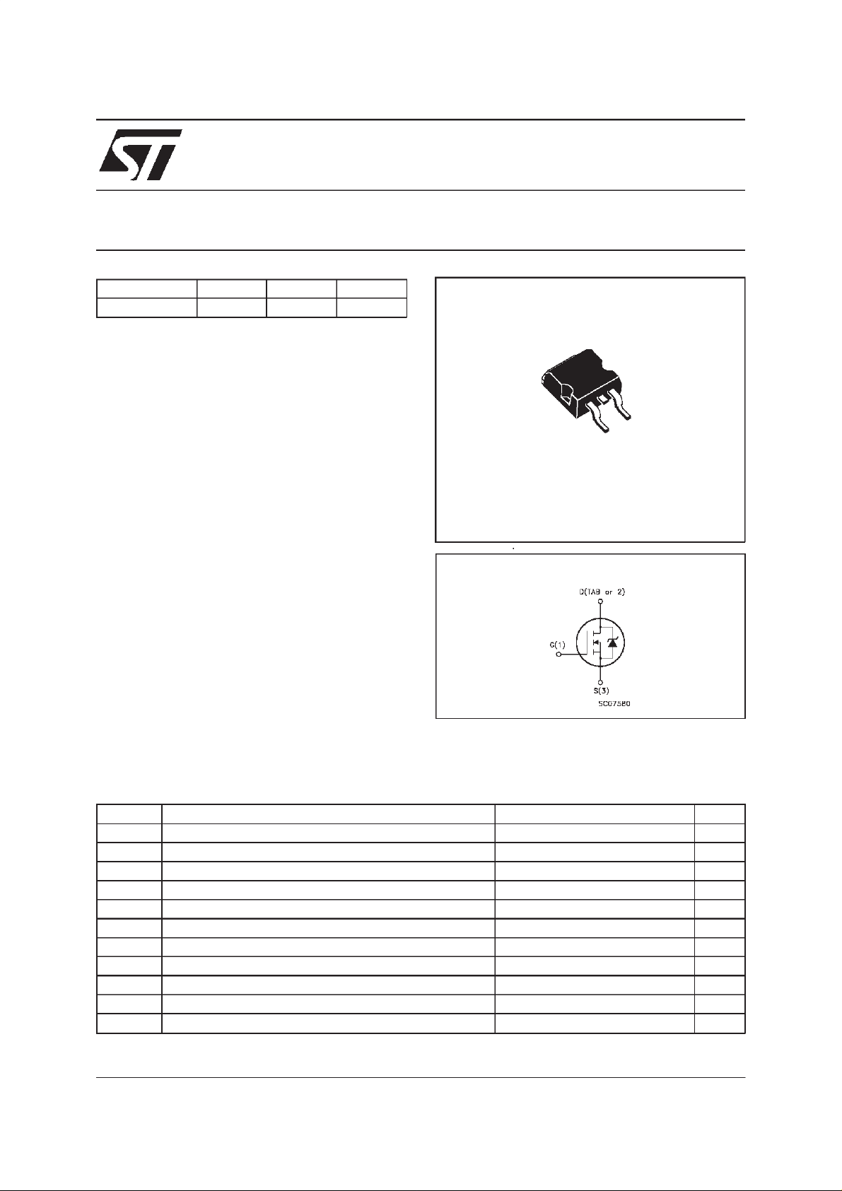
D2PAK
TO-263
(suffix ”T4”)
INTERNAL SCHEMATIC DIAGRAM
Symb o l Parameter Val u e Uni t
V
V
V
I
DM
P
Drain-source Voltage (VGS=0) 250 V
DS
Drain- gate Voltag e (RGS=20kΩ)250V
DGR
Gate-s ource Voltage ± 30 V
GS
Drain Curr ent (conti nuous) at Tc=25oC16A
I
D
Drain Curr ent (conti nuous) at Tc= 100oC10A
I
D
(•) Drain Curr ent (pulsed) 64 A
Total Dissipation at Tc=25oC140W
tot
Derating Factor 1.12 W/
1) Peak Diode Recove ry voltag e slope 5.5 V/ ns
dv/dt(
T
(•) Pulse width limited by safe operating area (1)I
St orage Temp er atur e -65 to 150
stg
Max. Operat ing Junc tion T emperature 150
T
j
≤
16A,di/dt≤200 A/µs, V
SD
≤
DD
V
(BR)DSS
,Tj≤T
JMAX
March 1999
o
C
o
C
o
C
1/8
STB16NB25
THERMAL DATA
R
thj-case
Rthj-a mb
R
thc-sink
T
AVALANCHE CHARACTERISTICS
Symbol Parameter Max Value Unit
I
AR
E
Ther mal Res istance Junc t ion-case Max
Ther mal Res istance Junc t ion-ambie nt Max
Ther mal Res istance Case -s ink Ty p
Maximum Lead Te m pe rat ur e For Solder ing Purpose
l
Avalanche Current, Repetitive or Not-Repetitive
(pulse width limited by T
Single Pulse A v alan c he Energy
AS
(starting T
=25oC, ID=IAR,VDD=50V)
j
max)
j
0.9
62.5
0.5
300
16 A
250 mJ
o
C/W
oC/W
o
C/W
o
C
ELECTRICAL CHARACTERISTICS
=25oC unless otherwisespecified)
(T
case
OFF
Symbol Parameter Test Conditions Min. Typ. Max. Unit
V
(BR)DSS
Drain-source
ID=250µAVGS= 0 250 V
Break dow n Volt age
I
DSS
I
GSS
Zero Gate Voltage
Drain Current (V
GS
Gat e- bod y Leakage
Current (V
DS
=0)
=0)
V
=MaxRating
DS
=MaxRating Tc=125oC
V
DS
V
=± 30 V
GS
1
10
100 nA
±
ON(∗)
Symbol Parameter Test Conditions Min. Typ. Max. Unit
V
GS(th)
R
DS(on)
Gate Threshold Voltage VDS=VGSID= 250 µ A 345V
Sta t ic Drain-sour c e On
VGS=10V ID= 8 A 0.22 0.28
Resistance
I
D(on)
On State Drain Current VDS>I
D(on)xRDS(on)max
16 A
VGS=10V
DYNAMIC
Symbol Parameter Test Conditions Min. Typ. Max. Unit
g
(∗)Forward
fs
Tr ansc on duc tance
C
C
C
Input Capacitanc e
iss
Out put Capacitance
oss
Reverse Transfer
rss
Capacit a nc e
VDS>I
D(on)xRDS(on)maxID
=8 A 4 S
VDS=25V f=1MHz VGS= 0 1000
250
40
µ
µA
Ω
pF
pF
pF
A
2/8
STB16NB25
ELECTRICAL CHARACTERISTICS
(continued)
SWITCHING ON
Symbol Parameter Test Conditions Min. Typ. Max. Unit
t
d(on)
Tur n-on Delay Tim e
Rise Time
t
r
VDD=125V ID=8A
R
=4.7
G
Ω
VGS=10V
12
12
(Resis t iv e Load, see f ig. 3)
Q
Q
Q
Tot al Gate C har ge
g
Gat e- Source Charge
gs
Gate-Drain Charg e
gd
VDD= 200 V ID=16A VGS=10V 29
9
11
38 nC
SWITCHING OFF
Symbol Parameter Test Conditions Min. Typ. Max. Unit
t
d(off)
Tur n-of f Delay Time
t
Fall T ime
f
VDD=125V ID=8A
=4.7 Ω VGS=10V
R
G
35
8
(Resis t iv e Load, see f ig. 3)
t
r(Voff)
t
t
Off-voltage Rise Tim e
Fall T ime
f
Cross-over Tim e
c
V
R
=200V ID=16A
CLAM P
=4.7 Ω VGS=10V
G
(Indu ct iv e Load, see fig . 5)
10
9
20
SOURCEDRAINDIODE
Symbol Parameter Test Conditions Min. Typ. Max. Unit
I
SDM
V
I
SD
Q
I
RRM
SD
t
Source-drain Current
(•)
Source-drain Current
16
64
(pulsed)
(∗)ForwardOnVoltage ISD=16A VGS=0 1.5 V
Reverse Recovery
rr
Time
Reverse Recovery
rr
ISD= 16 A di/dt = 100 A/µs
=50V Tj=150oC
V
DD
(see test circuit, fig. 5)
210
1.5
Charge
Reverse Recovery
14
Current
ns
ns
nC
nC
ns
ns
ns
ns
ns
A
A
ns
µC
A
(∗) Pulsed:Pulse duration = 300 µs, dutycycle 1.5%
(•) Pulse width limited by safeoperatingarea
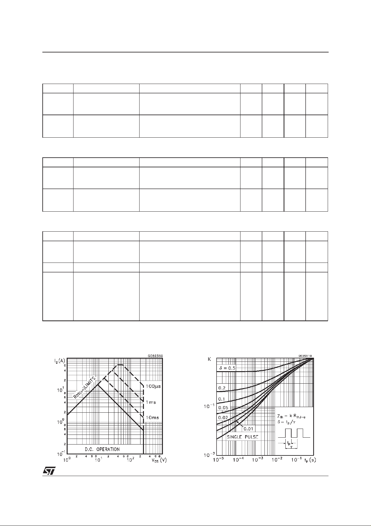
SafeOperating Area ThermalImpedance
3/8
 Loading...