

SGS Thomson Microelectronics STW150NF55, STP150NF55, STB150NF55 Datasheet
N-CHANNEL 55V - 0.005 Ω -120A D²PAK/TO-220/TO-247
TYPE
STB150NF55
STP150NF55
STP150NF55
■ TYPICAL R
■ SURFACE-MOUNTING D
V
DSS
55 V
55 V
55 V
(on) = 0.005 Ω
DS
POWER PACKAGE
DESCRIPTION
This Power MOSFET is the latest dev elo pment of
STMicroelectronis unique "Single Feature Size™"
strip-based process. The resulting transistor
shows extremely high packing density for low onresistance, rugged avalanche characteristics and
less critical alignment steps therefore a
remarkable manufacturing reproducibility.
APPLICATIONS
■ HIGH CURRENT, HIGH SWITCHING SPEED
■ SOLENOID AND RELAY DRIVERS
■ MOTOR CONTROL, AUDIO AMPLIFIERS
■ DC-DC & DC-AC CONVERTERS
■ AUTOMOTIVE
R
DS(on)
<0.006
Ω
<0.006
Ω
<0.006
Ω
2
PAK (TO-263)
I
D
120 A(**)
120 A(**)
120 A(**)
STB150NF55 STP150NF55
STW150NF55
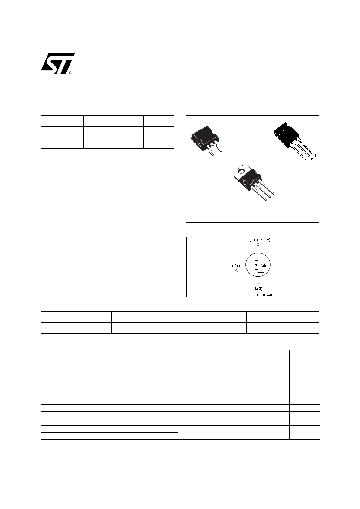
STripFET™ II POWER MOSFET
AUTOMOTIVE SPECIFIC
3
1
D2PAK
TO-263
(Suffix “T4”)
2
1
TO-220
INTERNAL SCHEMATIC DIAGRAM
TO-247
3
Ordering Information
STB150NF55T4 B150NF55
SALES TYPE MARKING PACKAGE PACKAGING
STP150NF55 P150NF55 TO-220 TUBE
STW150NF55 W150NF55 TO-247 TUBE
2
D
PAK
T APE & REEL
ABSOLUTE MAXIMUM RATINGS
Symbol Parameter Value Unit
V
DS
V
DGR
V
GS
(**) Drain Current (continuous) at T
I
D
I
D
(
I
DM
P
tot
Drain-source Voltage (VGS = 0)
Drain-gate Voltage (RGS = 20 kΩ)
55 V
55 V
Gate- source Voltage ± 20 V
= 25°C
C
Drain Current (continuous) at TC = 100°C
•)
Drain Current (pulsed) 480 A
Total Dissipation at TC = 25°C
120 A
106 A
300 W
Derating Factor 2.0 W/°C
(1)
dv/dt
E
AS
T
stg
T
j
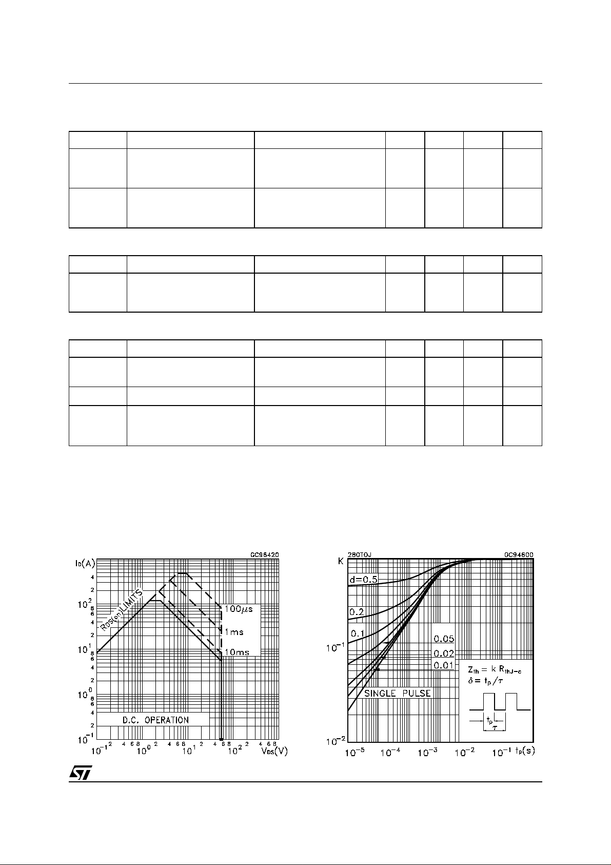
Pulse widt h l i m i ted by safe op erating area.
(
•)
(**) Curre nt Limited by Pac kage
Peak Diode Recovery voltage slope 8 V/ns
(2)
Single Pulse Avalanche Energy 850 mJ
Storage Temperature
Operating Junction Temperature
(1) ISD ≤120A, di/dt ≤200A/µs, VDD ≤ V
(2) Starting Tj = 25 oC, ID = 60 A, VDD = 30V
-55 to 175 °C
(BR)DSS
, Tj ≤ T
October 2002
JMAX
1/14
STB150NF55 STP150NF55 STW150NF55
THERMA L D ATA
Rthj-case
Rthj-amb
T
Thermal Resistance Junction-case
Thermal Resistance Junction-ambient
Maximum Lead Temperature For Soldering Purpose
l
Max
Max
Typ
0.5
62.5
300
°C/W
°C/W
°C
ELECTRICAL CHARACTERISTICS (T
= 25 °C unless otherwise specified)
case
OFF
Symbol Parameter Test Conditions Min. Typ. Max. Unit
I
V
(BR)DSS
Drain-source
= 250 µA VGS = 0
D
55 V
Breakdown Voltage
V
= Max Rating
DS
V
= Max Rating TC = 125°C
DS
V
= ± 20 V
GS
1
10
±100 nA
ON
(*)
I
DSS
I
GSS
Zero Gate Voltage
Drain Current (V
GS
Gate-body Leakage
Current (V
DS
= 0)
= 0)
Symbol Parameter Test Conditions Min. Typ. Max. Unit
V
GS(th)
R
DS(on)
Gate Threshold Voltage
Static Drain-source On
= VGS I
DS
V
= 10 V ID = 60 A
GS
= 250 µA
D
24V
0.005 0.006
V
Resistance
DYNAMIC
Symbol Parameter Test Conditions Min. Typ. Max. Unit
(*)
g
fs
C
iss
C
oss
C
rss
Forward Transconductance
Input Capacitance
Output Capacitance
Reverse Transfer
Capacitance
V
15 V ID= 60 A
DS =
= 25V, f = 1 MHz, VGS = 0
V
DS
160 S
4400
1050
350
µA
µA
Ω
pF
pF
pF
2/14
STB150NF55 STP150NF55 STW 150NF55
ELECTRICAL CHARACTERISTICS (continued)
SWITCHING ON
Symbol Parameter Test Conditions Min. Typ. Max. Unit
= 27.5 V ID = 60 A
t
d(on)
Turn-on Delay Time
t
r
Rise Time
V
DD
R
= 4.7 Ω VGS = 10 V
G
(Resistive Load, Figure 3)
Q
g
Q
gs
Q
gd
Total Gate Charge
Gate-Source Charge
Gate-Drain Charge
VDD=27.5 V ID=120A VGS= 10V
SWITCHING OFF
Symbol Parameter Test Conditions Min. Typ. Max. Unit
= 27.5 V ID = 60 A
t
d(off)
Turn-off Delay Time
t
f
Fall Time
V
DD
R
= 4.7Ω, V
G
GS
= 10 V
(Resistive Load, Figure 3)
SOURCE DRAIN DIODE
Symbol Parameter Test Conditions Min. Typ. Max. Unit
I
SD
I
SDM
V
SD
t
rr
Q
rr
I
RRM
(*)
Pulsed: P ul se duration = 300 µs, duty cycle 1.5 %.
(
•)Pulse width limited by s af e operatin g area.
Source-drain Current
(•)
Source-drain Current (pulsed)
(*)
Forward On Voltage
Reverse Recovery Time
Reverse Recovery Charge
Reverse Recovery Current
I
= 120 A VGS = 0
SD
= 120 A di/dt = 100A/µs
I
SD
V
= 25 V Tj = 150°C
DD
(see test circuit, Figure 5)
35
180
140
35
70
140
80
130
350
7.5
170 nC
120
480
1.5 V
ns
ns
nC
nC
ns
ns
A
A
ns
nC
A
Thermal ImpedanceSafe Operating Area
3/14
STB150NF55 STP150NF55 STW150NF55
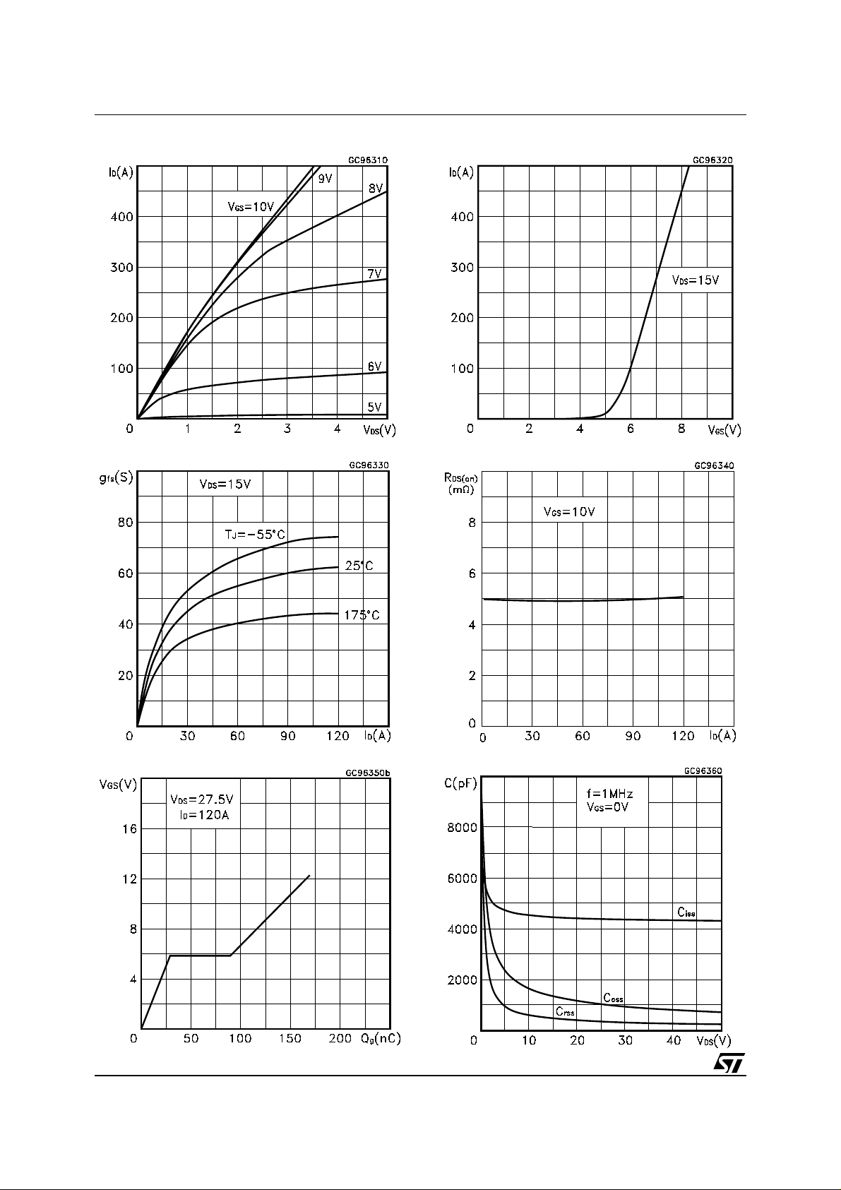
Output Characteristics Transfer Characteristics
Transconductance Static Drain-source On Resistance
Gate Charge vs Gate-source Voltage Capacitance Variations
4/14
STB150NF55 STP150NF55 STW 150NF55
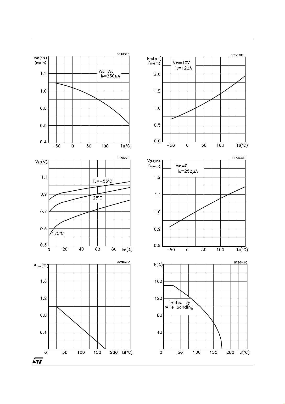
Normalized Gate Threshold Voltage vs Temperature Normalized on Resistance vs Temperature
Source-drain Diode Forward Characteristics Normalized Breakdown Voltage vs Temperature.
. .
Power Derating vs Tc Max Id Current vs Tc.
5/14
 Loading...