

ST9294
24K ROM HCMOS MCU WITH
ON SCRE EN DISPLA Y AND C LOSED -CAPTI ON DATA SLICER
FUNCTIONAL DESCRIPTION
Register oriented 8/ 16 bit C OR E with
RUN, WFI and HALT modes
Minimum instruct ion cycle time: 500ns
(12MHz internal)
12 to 32K bytes of ROM,
384/640 bytes of RAM ,
224 general purpose registers available as R AM,
accumulators or index registers (Register File)
42-lead Shrink DIP package or
56-lead Shrink DIP packag e
Interrupt handler and Serial P eripheral Interface
as standard features
31 (42 pin package) / 42 (56 pin package) fully
programmable I/O pins
34 character x15 rows software programmable
On Screen Dis play module with c olour, italic, underline, flash, transparent and fringe attribute
options
Digital Data Slicer extracting closed caption data
from video
8 8-bit PWM D/A outputs with repetition frequency 2 to 32kHz and 12V Open Drain
Capability
16 bit Timer wit h 8 bit Pres caler, able to be used
as a Watchdog Timer
16-bit programmable Slice Timer with 8-bit prescaler
3 channel Analog to Digital Converter, with integral sample and hold, fast 5.75µs conversion
time, 6-bit guaranteed resolution
Rich Instruct ion S et and 14 A ddressing modes
Division-by-Zero trap generati on
Versatile Development tools, including assembler,
linker, C-compiler, archiver, graphic oriented debugger and hardware emulators
Real Time Operating Sys tem
Windowed EPROM parts available for prototyp-
ing and pre-production development phases
(Ordering Information at the end of the Datasheet)
PSDIP42
PSDIP56
May 1993
This is Preliminary Data from SGS-THOMSON. Details are subject to change without notice.
1/6
ST9294
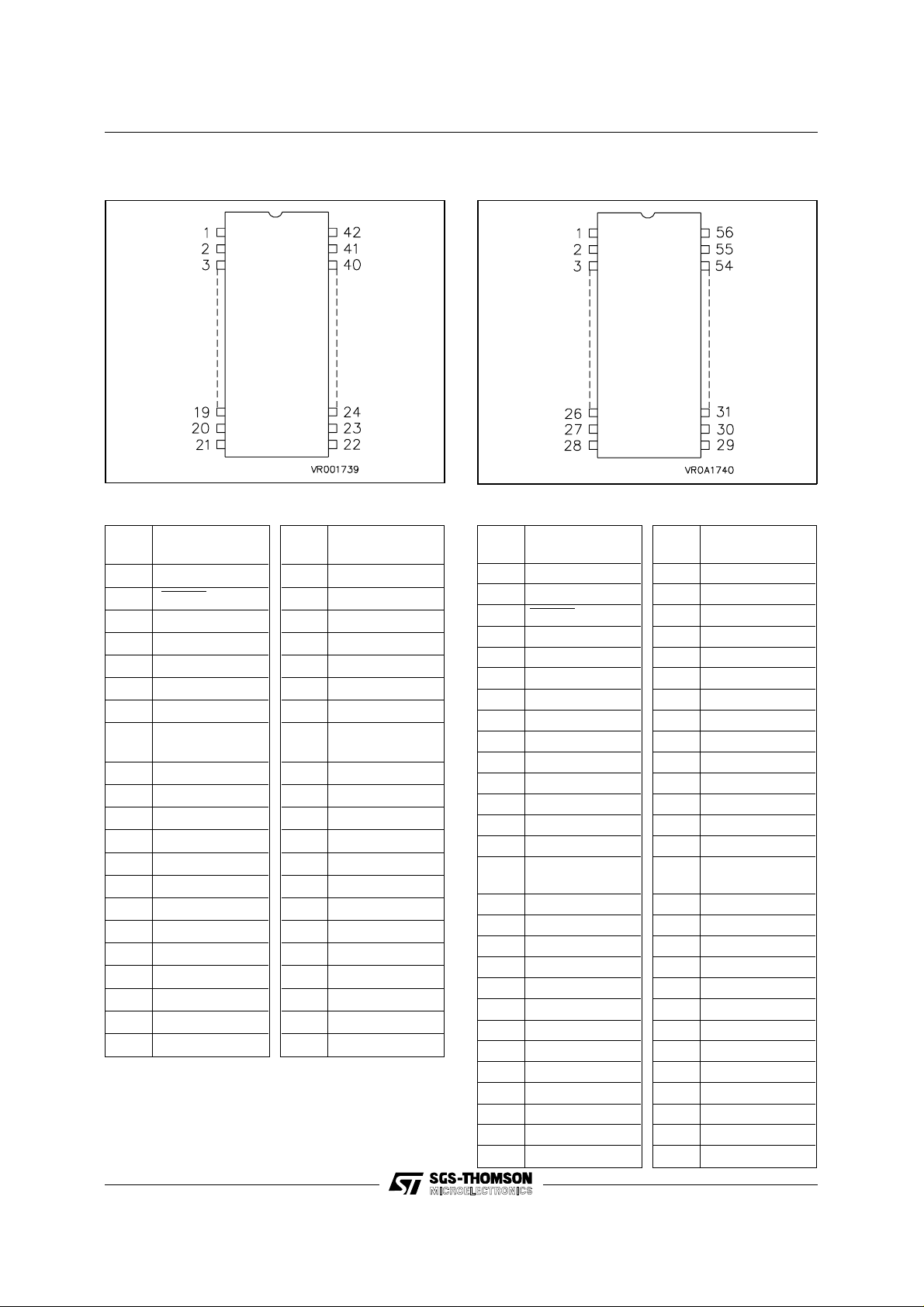
Figure 1a. 42 Pin Shrink DIP Pinout
ST9294J Pin Description
DD
Pin
name
Pin
42 P2.1/INT5/AIN1
41 P2.2/INT0/AIN2
40 P2.3/INT6/SDO
39 P2.4/NMI
38 P2.5/AIN3
37 OSCIN
36 OSCOUT
35 P4.7/PWM7/
EXTRG (AD)
34 P4.6/PWM6
33 P4.5/PWM5
32 P4.4/PWM4
31 P4.3/PWM3
30 P4.2/PWM2
29 P4.1/PWM1
28 P4.0/PWM0
27 VSYNC
26 HSYNC
25 AV
24 PLLR
23 PLLF
22 V
SS
Pin
1 P2.0/INT7
2 RESET
3 P0.7
4 P0.6
5 P0.5
6 P0.4
7 P0.3
8 P0.2
9 P0.1
10 P0.0
11 CCVideo
12 P3.6
13 P3.5
14 P3.4
15 P3.3/B
16 P3.2/G
17 P3.1/R
18 P3.0/FB
19 P5.1/SDIO
20 P5.0/SCK/INT2
21 V
2/6
DD
Pin
name
Figure 1b. 56 Pin Shrink DIP Pinout
ST9294N Pin Description
Pin
1 P2.1/INT5/AIN1
2 P2.0/INT7
3
4P0.7
5P0.6
6P0.5
7NC
8P0.4
9P0.3
10 P0.2
11 P0.1
12 P0.0
13 NC
14 V
15
16 P3.7
17 P3.6
18 P3.5
19 P3.4
20 P3.3/B
21 P3.2/G
22 P3.1/R
23 P3.0/FB
24 P5.3
25 P5.2
26 P5.1/SDIO
27 P5.0/SCK/INT2
28 V
name
RESET
DD
CCVideo
DD
Pin
Pin
56 P2.2/INT0/AIN2
55 P2.3/INT6/SDO
54 P2.4/NMI
53 P2.5/AIN3
52 P1.0
51 P1.1
50 P1.2
49 P1.3
48 P1.4
47 P1.5
46 P1.6
45 P1.7
44 OSCIN
43 OSCOUT
42
41 P4.6/PWM6
40 P4.5/PWM5
39 P4.4/PWM4
38 P4.3/PWM3
37 P4.2/PWM2
36 P4.1/PWM1
35 P4.0/PWM0
34 VSYNC
33 HSYNC
32 AV
31 PLLR
30 PLLF
29 V
Pin
name
P4.7/PWM7/
EXTRG (AD)
DD
SS

1.1 GENERAL DE SCRIPTI ON
The ST9294 is a ROM member of the ST9 fam ily of
microcontrollers, completely developed and produced by SGS-THOMSON Microelectronics using
a proprietary n-well HCMOS process.
The ROM parts are fully compatible with their
EPROM versions, which may be used for the prototyping and pre-production phases of development.
The nucleus of the ST9294 is the advanced Core
which includes the Central Processing Unit (C PU),
the Register File, a 16-bit Timer/Watchdog wit h 8bit Prescaler, a Serial P eripheral Interface support ing S-bus, I
2
C-bus and IM-bus Interface, plus two
8-bit I/O ports. The Core has independent m emory
and register buses allowing a high degree of pipelining to add to the efficiency of the code execution
speed of the extensive instruction s et.
The powerful I/O capabilities demanded by microcontroller applications are fulfilled by the ST9294
with up to 31/42 I/O lines dedicated to digital Input/Output. These lines are grouped into up to six
I/O Ports and can be configured on a bit basis under software control to provide timing, status sig-
ST9294
nals, timer inputs and outputs, analog inputs, external interrupts and serial or parallel I/O.
Three basic memory spaces are available to support this wide range of configurations: Program
Memory, Data Memory and the Register File,
which includes the control and status registers of
the on-chip peripherals.
The 16-bit Slice Timer with an 8-bit Presc aler.
The human interface is provided by the On S creen
Display module, this can produce up to 15 lines of
up to 34 characters from a ROM defined 128 character set. The 9x 13 charac ter can be modif ied by 4
different pixel sizes, with character rounding, and
formed into words with colour and format attributes.
Closed Caption control for the display of information transmitted through the video input is facilitated with the Data Slicer. This module has manual
and automatic Slicing levels for both Sync and
Data and allows the user to select the video line
containing the data relative to the Vertical synchronisation pulse.
Figure 1-2. ST9294 Block Diagram
12k / 24k Bytes
ROM
I/O PORT 0
8
Note : 42 SDIP shown
384 / 640 Bytes
RAM
MEMORY BUS ( Address & Data )
I/O PORT 2
( Analog Inputs )
6
256 Bytes
REGIST ER FILE
REGISTER BUS ( Address & Data )
A/D
CONVERTER
16-Bit TIMER / WATCHDOG + SPI
I/O PORT 3
7
VSYNC
CPU
ON SCREEN
DISPLAY
PLL
HSYNC
PLLR
PLLF
I/O PORT 4
P.W.M.
Outputs
AV
DD
SLICE
TIMER
P.W.M.
D/A
CONVERTER
8
DATA
SLICER
CC Video
I/O PORT 5
( SPI )
2
VR0A1749
3/6

ST9294
GENERAL DES CRIPTI ON (Continued)
Control of TV settings is able to be made with up to
eight 8-bit PWM outputs, with a frequency maximum of 23,437Hz at 8-bit resolution (INTCLK =
12MHz). Low resolutions with higher frequency operation can be programmed.
In addition th ere is a 3 cha nnel Analog to Digital Converter with integral sample and hold, fast 5.75µs conversion time and 6-bit guaranteed resolution.
1.2 PIN DESCRIPTI ON
VSYNC.
Vertical Synch.
Vertical video synchroni-
sation input to OSD. Positive or negative polarity.
HSYNC.
Horizontal Synch.
Horizontal video synchronisation input to OSD. Positive or negative polarity.
CCVideo.
Composite Video Input
. Input to Data
Slicer for Closed Caption extraction, 1V± 6dB or
2V± 3dB.
PLLF.
PLL Filter input.
Filter input for the OSD for
PLL feed-back.
PLLR .
PLL Resistor connection pin.
For resistor
connection to select the PLL gain adjust.
RESET.
ised by the Reset signal. With the deactivation of
Reset (input, active low).
The ST9 is initial-
RESET, program execution begins from the Program
memory location pointed to by the vector contained
in program memory locations 00h and 01h.
OSCIN, OSCOUT.
Oscillator (input and output).
These pins connect a parallel-resonant crystal
(24MHz maximum), or an external source to the
on-chip clock oscillator and buffer. OS CIN is the input of the oscillator inverter and internal clock ge nerator; OSCOUT is the output of the oscillator
inverter.
. Analog VDD of PLL. This pin mus t be tied to
AV
DD
externally to the ST9294.
V
DD
. Main Power Supply Voltage (5V±10%)
V
DD
V
. Digital Circuit Ground.
SS
P0.0-P0.7, P2.0-P2.5, P3.0-P3.6, P4.0-P4.7,
P5.0-P5.1 (J suffix)
P0.0-P0.7, P1.0-P1.7, P2.0-P2.5, P3.0-P3.7,
P4.0-P4.7, P5.0-P5.3 (N suffix)
put/Output, TTL or C MOS compat ible).
I/O Port Lines (In-
31/42 lines
grouped into I/O ports, bit programmable under
program control as general purpose I/O or as Alternate functions (see next section).
P4.0 - P4.7 are high voltage (12V) open drain
1.2.1I/O Port Alt ernate Fun ctions.
Each pin of the I/O ports of the ST9294 may assume software programmable Alternative Functions as shown in the Pin Configuration Drawings.
Table 1 shows the Functions alloc ated to e ach I/O
Port pin.
4/6

PIN DESCRIPTI ON (Continued)
Table 1-1. ST9294 I/O Port Alternative Function Summary
ST9294
I/O PORT
Port.bit 9294J 9294N
P0.0 I/O 10 12
P0.1 I/O 9 11
P0.2 I/O 8 10
P0.3 I/O 7 9
P0.4 I/O 6 8
P0.5 I/O 5 6
P0.6 I/O 4 5
P0.7 I/O 3 4
P1.0 I/O - 52
P1.1 I/O - 51
P1.2 I/O - 50
P1.3 I/O - 49
P1.4 I/O - 48
P1.5 I/O - 47
P1.6 I/O - 46
P1.7 I/O - 45
P2.0 INT7 I External Interrupt 7 with Schmitt Trigger 1 2
P2.1 INT5 I External Interrupt 5 with Schmitt Trigger 42 1
P2.1 AIN1 I A/D Analog Input 1 42 1
P2.2 INT0 I External Interrupt 0 41 56
P2.2 AIN2 I A/D Analog Input 2 41 56
P2.3 INT6 I External Interrupt 6 40 55
P2.3 SDO O MSPI Serial Data Output 40 55
P2.4 NMI I Non-Maskable Interrupt 39 54
P2.5 AIN3 I A/D Analog Input 3 38 53
P3.0 FB O Fast Blanking OSD output 18 23
P3.1 R O Red Video Colour OSD output 17 22
P3.2 G O Green Video Colour OSD output 16 21
P3.3 B O Blue Video Colour OSD output 15 20
Name Function Alternate Function
Pin Assignment
5/6

ST9294
PIN DESCRIPTI ON (Continued)
Table 1-1. ST9294 I/O Port Alternative Functi on Su mm ar y
I/O PORT
Port.bit 9294J 9294N
Name Function Alternate Function
Pin Assignment
P3.4 I/O 14 19
P3.5 I/O 13 18
P3.6 I/O 12 17
P3.7 I/O - 16
P4.0 PWM0 O PWM Output 0 28 35
P4.1 PWM1 O PWM Output 1 29 36
P4.2 PWM2 O PWM Output 2 30 37
P4.3 PWM3 O PWM Output 3 31 38
P4.4 PWM4 O PWM Output 4 32 39
P4.5 PWM5 O PWM Output 5 33 40
P4.6 PWM6 O PWM Output 6 34 41
P4.7 PWM7 O PWM Output 7 35 42
P4.7 EXTRG I A/D External Trigger 35 42
P5.0 SCK O SPI Serial Clock
P5.0 INT2 I External Interrupt 2
P5.1 SDIO O SPI Serial Data Input/Output
(1)
(1)
(1)
20 27
20 27
19 26
P5.2 I/O - 25
P5.3 I/O - 24
Notes.
1. The alternate functions of SCK/INT2 and SDIO may be swapped by using the SWAP Register Function.
2. Schmitt trigger options are available as a mask option for any input pin.
Information furnished is believed to be accurate and reliable. However, SGS-THOMSON Microelectronics assumes no responsability for the
consequences of use of such information nor for any infringement of patents or other rights of third parties which may result from its use. No
license is granted by implication or otherwise under any patent or patent rights of SGS-THOMSON Microelectronics. Specifications mentioned
in this publicat ion are subject t o change without not ice. This publication sup erse des a nd replaces all information previously supplied.
SGS-THOMSON Microelectronics products are not au thor ized for use as critical components in life support devices or systems without the
express written approval of SGS-THOMSON Microelectronics.
© 1995 SGS-THOMSON Microelectronics - All rights reserved.
2
Purchase of I
C Components by SGS-THOMSON Microelectronics conveys a license under the Philips I2C Patent.
Rights to use these components in an I
conforms to the I
2
C Standard Specification as defined by Philips.
2
C system is granted provided that the system
SGS-THOMSON Microelectronics Group of Companies
Australia - Brazil - France - Germany - Hong Kong - Italy - Japan - Korea - Malaysia - Malta - Morocco - The Netherlands
Singapore - Spain - Sweden - S wi t ze r la nd - Tai w an - T ha i la nd - Uni t ed K i ngd om - U. S. A .
6/6
 Loading...