

Datasheet ST90E158M9G0, ST90158P9C6, ST90158M9T1, ST90158M9Q6, ST90158M9 Datasheet (SGS Thomson Microelectronics)
...
January 2000 1/190
Rev. 3.0
ST90158 - ST90135
8/16-BIT MCU FAMILY WITH
UP TO 64K ROM/OTP/EPROM AND UP TO 2K RAM
■ Register File based 8/16 bit Core Architecture
with RUN, WFI, SLOW and HALT modes
■ 0 - 16 MHz Operation @ 5V±10%, -40°Cto
+85°C and 0°C to +70°C Operating
Temperature Ranges
■ 0 - 14 MHz Operation @ 3V±10% and 0°Cto
+70°C Operating Temperature Range
■ Fully Programmable PLL Clock Generator, with
Frequency Multiplication and low frequency,
low cost external crystal
■ Minimum 8-bit InstructionCycle time:83ns - (@
24 MHz internal clock frequency)
■ Minimum 16-bit Instruction Cycle time: 250ns -
(@ 24 MHz internal clock frequency)
■ Internal Memory:
– EPROM/OTP/ROM 16/24/32/48/64K bytes
– ROMlessversion available
– RAM512/768/1K/1.5K/2K bytes
■ Maximum External Memory: 64K bytes
■ 224 general purpose registers available as
RAM, accumulators or index pointers (register
file)
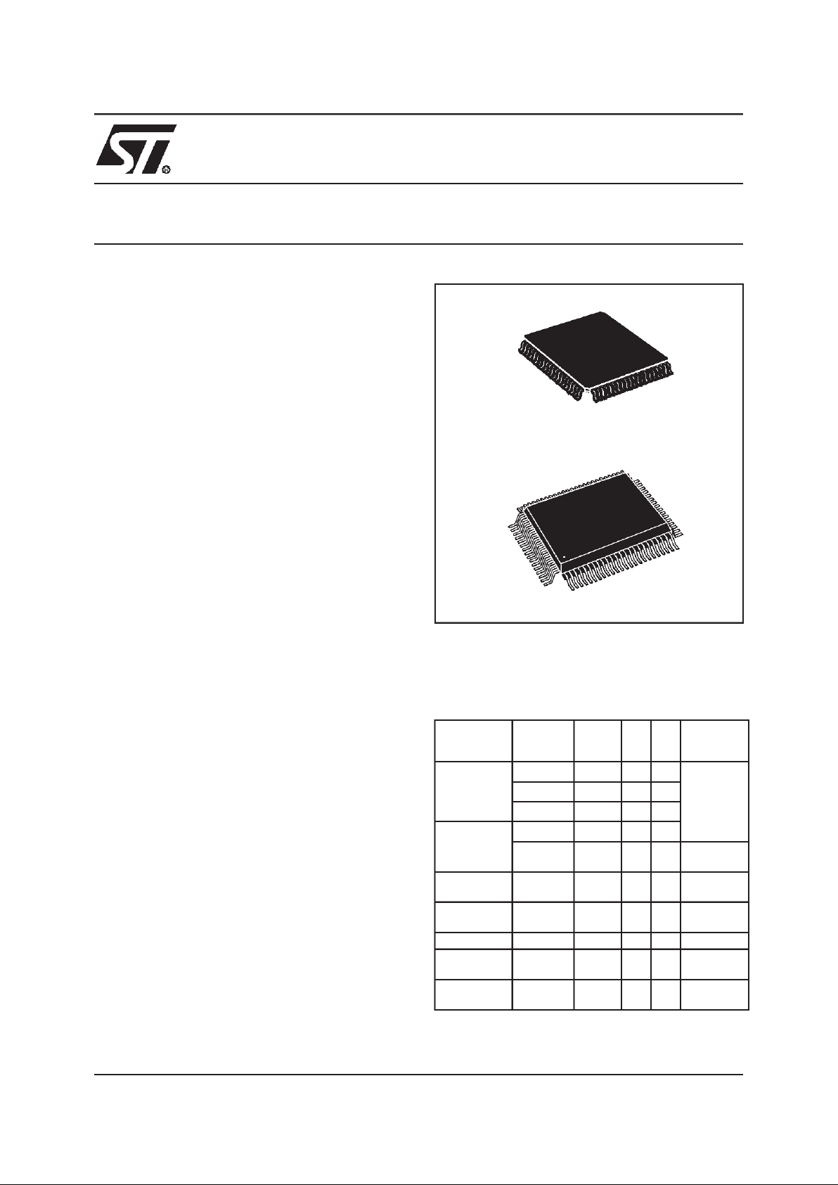
■ 80-pin Plastic Quad Flat Package and 80-pin
Thin Quad Flat Package
■ 67 fully programmable I/O bits
■ 8 external and 1 Non-Maskable Interrupts
■ DMA Controller and Programmable Interrupt
Handler
■ Single Master Serial Peripheral Interface
■ Two 16-bit Timers with 8-bit Prescaler, one
usable as a Watchdog Timer (software and
hardware)
■ Three (ST90158) or two (ST90135) 16-bit
Multifunction Timers, each with an 8 bit
prescaler, 12 operating modes and DMA
capabilities
■ 8 channel 8-bitAnalog toDigital Converter, with
Automatic voltage monitoring capabilities and
external reference inputs
■ Two (ST90158) or one (ST90135) Serial
Communication Interfaces with asynchronous,
synchronous and DMA capabilities
■ Rich Instruction Set with 14 Addressing modes
■ Division-by-Zero trap generation
■ Versatile Development Tools, including
Assembler, Linker, C-compiler, Archiver,
Source Level Debugger and Hardware
Emulators with Real-Time Operating System
available from Third Parties
DEVICE SUMMARY
DEVICE
Program
Memory
(Bytes)
RAM
(Bytes)
MFT SCI PACKAGE
ST90135
16K ROM 512 2 1
PQFP80
24K ROM 768 2 1
32K ROM 1K 2 1
ST90158
48K ROM 1.5K 3 2
64k ROM 2K 3 2
PQFP80/
TQFP80
ST90E158
64K
EPROM
2K 3 2 CQFP80
ST90E158LV
64K
EPROM
2K 3 2 CQFP80
ST90T158 64K OTP 2K 3 2 PQFP80
ST90T158LV 64K OTP 2K 3 2
PQFP80/
TQFP80/
ST90R158 ROMless 2K 3 2
PQFP80/
TQFP80
PQFP80
TQFP80
9

2/190
Table of Contents
190
9
1 GENERAL DESCRIPTION . . . . . . ................................................ 6
1.1 INTRODUCTION . . . . . . . . . . . . . ............................................ 6
1.1.1 ST9+ Core . . . ..................................................... 6
1.1.2 Power Saving Modes . . . .. . . . . . .. . ................................... 6
1.1.3 system Clock . . . . . .. .. . . . . .........................................6
1.1.4 I/O Ports . . . . . . . . . .. . . . ............................................ 6
1.1.5 Multifunction Timers (MFT) . . . ......................................... 7
1.1.6 Standard Timer (STIM) . . . . . . . . . . . .. . . . . . . . . . . . . . . . . . . . . . . . . . . . . . . . . . . 7
1.1.7 Watchdog Timer (WDT) . . . . . . . . . .....................................7
1.1.8 Serial Peripheral Interface (SPI) . . .. . ................................... 7
1.1.9 Serial Communications Controllers (SCI) . . . . . . . . . . . . ..................... 7
1.1.10 Analog/Digital Converter (ADC) . . . . . . . . . . . .. . . . . . .. . . . . . .. . ............ 7
1.2 PIN DESCRIPTION . . .................................................... 10
1.3 I/O PORT PINS . . . . . . . . . . . . . . . . . ........................................13
2 DEVICE ARCHITECTURE . . . . . . . . . . ........................................... 18
2.1 CORE ARCHITECTURE . . . . . . .. . .. .. . . . . . ................................18
2.2 MEMORY SPACES . . . . . . . . .. . . . . ........................................ 18
2.2.1 Register File . . . . . . . .. . . . . . .. . . . . . .. . .............................. 18
2.2.2 Register Addressing . . . . ............................................20
2.3 SYSTEM REGISTERS . . . .. . . . . . . . . . . . . .. . . . .............................. 21
2.3.1 Central Interrupt Control Register .. . . . . . . . . . ........................... 21
2.3.2 Flag Register . . . . . . ............................................... 22
2.3.3 Register Pointing Techniques . ........................................23
2.3.4 Paged Registers . . . .. . . . . . . . .. .. . . . . . . . . . . . . . . . . . . . . . . . . . . . . . .. . . . . 26
2.3.5 Mode Register . . . . . ............................................... 26
2.3.6 Stack Pointers . . . . . . . . . .. . .. . . . . . . .................................27
2.4 MEMORY ORGANIZATION . . . . . . . . . . . . . . . ................................. 29
2.5 MEMORY MANAGEMENT UNIT . . . . . . . .. . .................................. 30
2.6 ADDRESS SPACE EXTENSION . . . . . .. . . . . . . .. . . . . . . . . . . . . . . .. . . . . . .. . . . . . . 31
2.6.1 Addressing 16-Kbyte Pages . .. . . . . . . ................................. 31
2.6.2 Addressing 64-Kbyte Segments . . . . . .................................. 32
2.7 MMU REGISTERS . ...................................................... 32
2.7.1 DPR[3:0]: Data Page Registers . . . . . . . . . . . . . . . . . . .. . . . . . .. . ........... 32
2.7.2 CSR: Code Segment Register ........................................34
2.7.3 ISR: Interrupt Segment Register . . . . .. . . . .............................. 34
2.7.4 DMASR: DMA Segment Register . . . . . . . . .............................. 34
2.8 MMU USAGE . . . . .. . . . . . .. . . . . . . . . . . . . . ................................. 36
2.8.1 Normal Program Execution . . . . . . . . .. . . . . . .. . . . . . .. . . . . ............... 36
2.8.2 Interrupts . . . . . . . . . . . . . . . . . .. . . . . . . . . .............................. 36
2.8.3 DMA . . . . . . .. . . . . . .. . . . . . .. . . . . . .. . . . . ........................... 36
3 REGISTER AND MEMORY MAP ................................................ 37
3.1 MEMORY CONFIGURATION . . . . . . . . . . . . . .................................37
3.2 EPROM PROGRAMMING . . . . . .. . . . . . . . . . .. . . . . . . . . . .. .. . . . . . . .. . . . . . . . . . . 37
3.3 MEMORY MAP . . . . . .. .. . ...............................................39
3.4 ST90158/135 REGISTER MAP . . . . . . .. . . . .................................. 40
4 INTERRUPTS . . ............................................................. 48
4.1 INTRODUCTION . . . . . . . . . . . . . ...........................................48
4.2 INTERRUPT VECTORING ................................................ 48

3/190
Table of Contents
9
4.2.1 Divide by Zero trap . . . . .. . .. . . . . . .. ................................. 48
4.2.2 Segment Paging During Interrupt Routines . ............................. 49
4.3 INTERRUPT PRIORITY LEVELS . . . . . . . . .. . . . . . .. . . . . . .. . . . . . .. . . . . . .. . . . . . 49
4.4 PRIORITY LEVEL ARBITRATION . .. ........................................49
4.4.1 Priority level 7 (Lowest) . . . . . . . . . . .. . . . . . .. . . . . . .. . . . . . .. . . . . . .. . . . . . 49
4.4.2 Maximum depth of nesting . . . ........................................ 49
4.4.3 Simultaneous Interrupts . . . . . . .. . . . . ................................. 49
4.4.4 Dynamic Priority Level Modification . . . . .. . . . . . .. . . . . . .. .. . . . . . . . . . .. . . . 50
4.5 ARBITRATION MODES . . . . . . . .. .. . . . . . . .................................. 50
4.5.1 Concurrent Mode . . .. . . . . . . . . . . . . . . . . . . . . .. . . . . . . . . .. . . . . . . .. .. . . . . 50
4.5.2 Nested Mode . . . . . . ............................................... 53
4.6 EXTERNAL INTERRUPTS . . . . . . . . .. . . . . . .. . .............................. 55
4.7 TOP LEVEL INTERRUPT . . . . . . . . .. . . . . . . .................................57
4.8 ON-CHIP PERIPHERAL INTERRUPTS . . . .. . . . . . .. . . . . . .. . . . . . .. . ........... 57
4.9 INTERRUPT RESPONSE TIME . ...........................................58
4.10INTERRUPT REGISTERS . . ...............................................59
5 ON-CHIP DIRECT MEMORY ACCESS (DMA) . . . . .................................. 63
5.1 INTRODUCTION . . . . . . . . . . . . . ...........................................63
5.2 DMA PRIORITY LEVELS . . . ...............................................63
5.3 DMA TRANSACTIONS .. . . . . . . . . . ........................................64
5.4 DMA CYCLE TIME . . . . . . . .. .. . . . . ........................................ 66
5.5 SWAP MODE . . . . . . . .. . . . ...............................................66
5.6 DMA REGISTERS . . . . . . . . . . . . ...........................................67
6 RESET AND CLOCK CONTROL UNIT (RCCU) . . . .................................68
6.1 INTRODUCTION . . . . . . . . . . . . . ...........................................68
6.2 CLOCK CONTROL UNIT . . . . . . . ...........................................68
6.2.1 Clock Control Unit Overview . . ........................................68
6.3 CLOCK MANAGEMENT . . .. .. . . . . ........................................ 69
6.3.1 PLL Clock Multiplier Programming . . . . .................................70
6.3.2 CPU Clock Prescaling . . . . . . . . . . . .. . . . . . .. . . . . . .. . . . . . .. . . . . . .. . . . . . 70
6.3.3 Peripheral Clock . . . . . . . . . . .. .. . . . . . . .. . . . . . . . . . . . . . . . . . . . . . . . .. . . . . 70
6.3.4 Low Power Modes . . . . . . . . . . . . . . . . . . . . . . . . . . . . . . . . . . . . . . . .. ........ 71
6.3.5 Interrupt Generation . . . . . . . . . . . . . . . . . . . . . . . . . . . . .................... 71
6.4 CLOCK CONTROL REGISTERS . . . . . . .. . . . . . . .............................. 74
6.5 OSCILLATOR CHARACTERISTICS . . . . . . . . . . . .............................. 77
6.6 RESET/STOP MANAGER . . . . . . ...........................................79
6.6.1 RESET Pin Timing . . . . . . . . . . . . . . . . ................................. 80
6.7 EXTERNAL STOP MODE . . ...............................................80
7 EXTERNAL MEMORY INTERFACE (EXTMI) . . . . . . . . . . . . . . . . . . . . . . . . . . . . . . . . . . . . . . 81
7.1 INTRODUCTION . . . . . . . . . . . . . ...........................................81
7.2 EXTERNAL MEMORYSIGNALS . . . . . . . . . . . .. . . . . ........................... 82
7.2.1 AS: Address Strobe . . . .. . . . . . . . . . . . . . . . . ........................... 82
7.2.2 DS: Data Strobe . . . . ...............................................82
7.2.3 DS2: Data Strobe 2 . . . . . . . .. . . . . . .. . . . . .. . . . . . . . .. . . . . .. . . . . . .. . . . . . 82
7.2.4 RW: Read/Write . . . . ............................................... 85
7.2.5 BREQ, BACK: Bus Request, Bus Acknowledge . . . . .. . . . . . .. . . . . . . ........ 85
7.2.6 PORT 0 . . . . . . .................................................... 86

4/190
Table of Contents
1
7.2.7 PORT 1 . . . . . . .................................................... 86
7.2.8 WAIT: External Memory Wait . . . . . . . . . . . . . . . . . . .. . . . . . . ............... 86
7.3 REGISTER DESCRIPTION . ............................................... 87
8 I/O PORTS . . . . . . . . . . . . . . . . . . . . . . . . . . ........................................ 90
8.1 INTRODUCTION . . . . . . . . . . . . . ...........................................90
8.2 SPECIFIC PORT CONFIGURATIONS .. . . . . . . . . . . . . . . . . . . . . . . . . . . . . . ........ 90
8.3 PORT CONTROL REGISTERS . . . . . . . . . . .. .. . . . . ........................... 90
8.4 INPUT/OUTPUT BIT CONFIGURATION . . . . . . . . . . . . . . . . . . . . . . . . . .. . .. . . . . . .. . 91
8.5 ALTERNATE FUNCTION ARCHITECTURE . . .. . . . . . . . . . . . . . . . . . . . . ........... 95
8.5.1 Pin Declared as I/O . . ............................................... 95
8.5.2 Pin Declared as an Alternate Input . . . . . . . . . . . .. . . . . . . . . .. . . . . . . . . . . . . . . 95
8.5.3 Pin Declared as an Alternate Function Output . . .. . . . . .. . . . . . . .. . . . . . . . . . . 95
8.6 I/O STATUS AFTER WFI,HALT AND RESET . . . . . . . . . . . . . . . . . . . . . ............ 95
9 ON-CHIP PERIPHERALS . . . . . . . . . . . ...........................................96
9.1 TIMER/WATCHDOG (WDT) . . . . . .. . . . . . . .................................. 96
9.1.1 Introduction . . . . . . . .. . . . ...........................................96
9.1.2 Functional Description . . . . . . ........................................97
9.1.3 Watchdog Timer Operation . . . . . . . ....................................98
9.1.4 WDT Interrupts ................................................... 100
9.1.5 Register Description . . . . ...........................................101
9.2 MULTIFUNCTION TIMER (MFT) . . . . . . . .. . . . . . . . . . . . . . . . ................... 103
9.2.1 Introduction . . . . . . . .. . . . ..........................................103
9.2.2 Functional Description . . . . . . .......................................105
9.2.3 Input Pin Assignment . . . . . .. . . . . . . ................................. 108
9.2.4 Output Pin Assignment . . . . . .. .. . . . . . . . . . . . . . . . . . . . . . . . . . . . . . . . .. . . . 112
9.2.5 Interrupt and DMA . . . . . . . . . . .. . . . . ................................114
9.2.6 Register Description . . . . ...........................................116
9.3 STANDARD TIMER (STIM) . ..............................................127
9.3.1 Introduction . . . . . . . .. . . . ..........................................127
9.3.2 Functional Description . . . . . . .......................................128
9.3.3 Interrupt Selection . . . .............................................. 129
9.3.4 Register Mapping . . . . . . . ..........................................129
9.3.5 Register Description . . . . ...........................................130
9.4 SERIAL PERIPHERAL INTERFACE (SPI) . . . . . . . . . . . . . . . .. . . . . . .. . .......... 131
9.4.1 Introduction . . . . . . . .. . . . ..........................................131
9.4.2 Device-Specific Options . . . . . . . . . . . . . . . . . . . . . . . . . . . . . .. . . . . . . .. . . . . . 131
9.4.3 Functional Description . . . . . . .......................................132
9.4.4 Interrupt Structure . . . .............................................. 133
9.4.5 Working With Other Protocols . . . . ................................... 134
9.4.6 I2C-bus Interface . . . .............................................. 134
9.4.7 S-Bus Interface . . . . . .. . . . . . .. . . . . . .. . . . . . . .. .. . ................... 137
9.4.8 IM-bus Interface . . . . . . . . . . . .......................................138
9.4.9 Register Description . . . . ...........................................139
9.5 SERIAL COMMUNICATIONS INTERFACE (SCI) . . . .. . . . . . . . . . . . . . . . . . . . . . . . .. 141
9.5.1 Introduction . . . . . . . .. . . . ..........................................141
9.5.2 Functional Description . . . . . . .......................................142
9.5.3 SCI Operating Modes . . . . . .. . . . . . .. . . . . . .. . . . . . .. . . . . . .. . . . . . . .. . . . 143
9.5.4 Serial Frame Format . . . . . . . . . . . . . . . . . . . .. . . . . . . . .. . . . . .. . . . . . .. . . . . 146

5/190
Table of Contents
1
9.5.5 Clocks And Serial Transmission Rates . ................................ 149
9.5.6 SCI Initialization Procedure . . . . . . . .. . . . ............................. 149
9.5.7 Input Signals . . . . . . . . . . . . . . .......................................151
9.5.8 Output Signals . . . . . . .. . . . . . . . . . . . . .. . . . . . . . . . . . . . . .. . . . . . . ....... 151
9.5.9 Interrupts and DMA . . . . . . . . . .......................................152
9.5.10 Register Description . ..............................................155
9.6 EIGHT-CHANNEL ANALOG TO DIGITAL CONVERTER (A/D) . . . . . . . . . . . . . . . . . .. 166
9.6.1 Introduction . . . . . . . .. . . . ..........................................166
9.6.2 Functional Description . . . . . . .......................................167
9.6.3 Interrupts . . . . . . . . . . . . . . . . . .. . . . . . . . . ............................. 169
9.6.4 Register Description . . . . ...........................................170
10 ELECTRICAL CHARACTERISTICS . . . . ........................................ 174
11 GENERAL INFORMATION ................................................... 188
11.1PACKAGE MECHANICALDATA . . . . . . . . . . . . . . . . . .......................... 188
11.280-PIN PLASTIC QUADFLAT PACKAGE . . . . ................................188
11.3ORDERING INFORMATION . . . . . . . . . . . . . ................................. 189

6/190
ST90158 - GENERAL DESCRIPTION
1 GENERAL DESCRIPTION
1.1 INTRODUCTION
The ST90158 and ST90135 microcontrollers are
developed and manufactured by STMicroelectronics using a proprietary n-well CMOS process.
Their performance derives from the use of a flexible 256-register programming model for ultra-fast
context switching and real-time event response.
The intelligent on-chip peripherals offload the ST9
core from I/O and data management processing
tasks allowing critical application tasks to get the
maximum use of core resources. The new-generation ST9 MCU devices now also support low
power consumption and low voltage operation for
power-efficient and low-cost embedded systems.
1.1.1 ST9+ Core
The advanced Core consists of the Central
Processing Unit(CPU), the RegisterFile, the Interrupt and DMA controller, and the Memory Management Unit. The MMU allows addressing of up
to 4 Megabytes of program and data mapped into
a single linear space.
Four independent buses are controlled by the
Core: a 16-bit memory bus, an 8-bit register data
bus, an 8-bit register address bus and a 6-bit interrupt/DMA bus which connects the interrupt and
DMA controllersin theon-chip peripherals with the
core.
This multiple bus architecture makes the ST9 family deviceshighly efficient foraccessing onand offchip memory and fast exchange of data with the
on-chip peripherals.
The general-purpose registers canbe used as accumulators, index registers, or address pointers.
Adjacent registerpairs make up 16-bit registersfor
addressing or 16-bit processing. Although theST9
has an 8-bit ALU, the chip handles 16-bit operations, including arithmetic, loads/stores, and memory/register and memory/memory exchanges.
1.1.2 Power Saving Modes
To optimize performance versus power consumption, a range of operating modes can be dynamically selected.
Run Mode. This is the full speed execution mode
with CPUand peripherals running at the maximum
clock speed delivered by the Phase Locked Loop
(PLL) of the Clock Control Unit (CCU).
Slow Mode. Power consumption can be significantly reduced byrunning the CPU and the peripherals at reduced clock speed using the CPU Prescaler and CCU Clock Divider(PLL not used) or by
using the CK_AF external clock.
Wait For Interrupt Mode. The Wait For Interrupt
(WFI) instruction suspends program executionuntil an interrupt request is acknowledged. During
WFI, the CPU clock is halted while the peripheral
and interrupt controller keep running at a frequency programmable via the CCU. In this mode, the
power consumption of the device can be reduced
by more than 95% (Low Power WFI).
Halt Mode. When executing the HALT instruction,
and if the Watchdog is not enabled, the CPU and
its peripherals stop operating and the status of the
machine remains frozen (the clock is also
stopped). A reset is necessary to exit from Halt
mode.
1.1.3 system Clock
A programmable PLL Clock Generator allows
standard 3 to 5MHz crystals tobe used to obtaina
large range of internal frequencies up to 24 MHz.
1.1.4 I/O Ports
The I/O lines are grouped into up to nine 8-bit I/O
Ports and can be configured on a bit basis to provide timing,status signals, an address/databus for
interfacing to external memory, timer inputs and
outputs, analog inputs, external interrupts and serial or parallel I/O.
9

7/190
ST90158 - GENERAL DESCRIPTION
1.1.5 Multifunction Timers (MFT)
Each multifunction timer has a 16-bit Up/Down
counter supported by two 16-bit Compare registers and two 16-bit input capture registers. Timing
resolution canbeprogrammed using an 8-bit prescaler. Multibyte transfers between the peripheral
and memory aresupported by two DMA channels.
1.1.6 Standard Timer (STIM)
The Standard Timer includes a programmable 16bit downcounter andan associated 8-bit prescaler
with Single and Continuous counting modes.
1.1.7 Watchdog Timer (WDT)
The Watchdog timer can be used to monitor system integrity. When enabled, it generates a reset
after a timeout period unless the counter is refreshed by the application software. For additional
security, watchdog function can be enabled by
hardware using a specific pin.
1.1.8 Serial Peripheral Interface (SPI)
The SPI bus is used to communicate with external
devices via the SPI, or I C bus communication
standards. The SPI uses oneor two lines for serial
data and a synchronous clock signal.
1.1.9 Serial Communications Controllers (SCI)
Each SCI provides a synchronous or asynchronous serial I/O port using two DMA channels.
Baud rates and data formats are programmable.
1.1.10 Analog/Digital Converter (ADC)
The ADCs provide up to 8 analog inputs with onchip sample and hold. The analog watchdog generates an interrupt when the input v oltage moves
out of a preset threshold.
9

8/190
ST90158 - GENERAL DESCRIPTION
Figure 1. ST90158 Block Diagram
256 bytes
Register File
RAM
up to 2 Kbytes
ST9+ CORE
8/16 bits
CPU
Interrupt
Management
MEMORY BUS
RCCU
REGISTER BUS
WATCHDOG
OSCIN
OSCOUT
RESET
INTCLK
CKAF
AS
WAIT
NMI
R/W
DS
MFT1
MFT0
T0OUTA
T0OUTB
T0INA
T0INB
EPROM/
ROM/OTP
up to64 Kbytes
WDIN
WDOUT
HW0SW1
All alternate functions (
Italic characters
) are mapped on Port2 through Port9
INT0-7
MFT3
T3OUTA
T3OUTB
T3INA
T3INB
T1OUTA
T1OUTB
T1INA
T1INB
ADDRESS
DATA
Port0
SDI
SDO
SCK
P1[7:0]
P0[7:0]
SPI
I
2
C/IM Bus
STIM
SCI0
EXTRG
AIN[7:0]
TX0CKIN
RX0CKIN
S0IN
DCD0
S0OUT
CLK0OUT
RTS0
STOUT
ADDRESS
Port1
Fully Prog.
I/Os
A/D
Converter
with analog
watchdog
P0[7:0]
P1[7:0]
P2[6:0]
P4[7:0]
P5[7:3], P5.1
P6[6:0]
P7[7:0]
P8[7:0]
P9[7:4], P9[2:0]
SCI1
TX1CKIN
RX1CKIN
S1IN
DCD1
S1OUT
CLK1OUT
RTS1
9

9/190
ST90158 - GENERAL DESCRIPTION
Figure 2. ST90135 Block Diagram
256 bytes
Register File
RAM
up to 1 Kbyte
ST9+ CORE
8/16 bits
CPU
Interrupt
Management
MEMORY BUS
RCCU
ADDRESS
DATA
Port0
REGISTER BUS
WATCHDOG
OSCIN
OSCOUT
RESET
INTCLK
CKAF
AS
WAIT
NMI
R/W
DS
SDI
SDO
SCK
P1[7:0]
P0[7:0]
MFT3
MFT1
SPI
I
2
C/IM Bus
T1OUTA
T1OUTB
T1INA
T1INB
STIM
SCI0
ROM
up to 32
Kbytes
EXTRG
AIN[7:0]
TX0CKIN
RX0CKIN
S0IN
DCD0
S0OUT
CLK0OUT
RTS0
STOUT
All alternate functions (
Italic characters
) are mapped on Port2 through Port9
INT0-7
ADDRESS
Port1
Fully Prog.
I/Os
T3OUTA
T3OUTB
T3INA
T3INB
WDIN
WDOUT
HW0SW1
A/D
Converter
with analog
watchdog
P0[7:0]
P1[7:0]
P2[6:0]
P4[7:0]
P5[7:3], P5.1
P6[6:0]
P7[7:0]
P8[7:0]
P9[7:4], P9[2:0]
9

10/190
ST90158 - GENERAL DESCRIPTION
9
1.2 PIN DESCRIPTION
AS: Address Strobe (output, active low, 3-state).
Address Strobe is pulsed low once at the beginning of each memory cycle. The rising edge of AS
indicates that address, Read/Write (R/W), and
Data Memory signals are valid for memory transfers. Underprogram control, AS canbe placed in a
high-impedance statealong withPort 0, Port 1and
Data Strobe (DS).
DS: Data Strobe (output, active low, 3-state). Data
Strobe provides thetiming for data movement toor
from Port 0 for each memory transfer. During a
write cycle, data out is valid at the leading edge of
DS. During a readcycle, Data In must be valid prior to the trailing edge of DS. When the ST90158
accesses on-chip memory, DS isheld high during
the whole memory cycle. It can be placed ina high
impedance state along with Port 0, Port 1 and AS.
RESET: Reset (input, active low).The ST9+ is initialised by the Reset signal. With the deactivation
of RESET, program execution begins from the
memory location pointed to by the vector contained in memory locations 00h and 01h.
R/W: Read/Write (output, 3-state).Read/Write determines the direction of data transfer for external
memory transactions. R/W is low when writing to
external memory, and high for all other transactions. It can be placed in high impedance state
along with Port 0, Port 1, ASand DS.
OSCIN, OSCOUT: Oscillator (input and output).
These pins connect a parallel-resonant crystal (3
to 5 MHz), or an external source to the on-chip
clock oscillator and buffer. OSCIN is the input of
the oscillator inverter and internal clock generator;
OSCOUT is the output of theoscillator inverter.
HW0_SW1: When connectedto VDDthrough a 1K
pull-up resistor, the software watchdog option is
selected. When connected to VSSthrough a 1K
pull-down resistor, the hardware watchdog option
is selected.
VPP: Programming voltage for EPROM/OTP devices. Must be connected to VSSin user mode
through a 10Kohm resistor.
AVDD: Analog VDDof the Analog to Digital Con-
verter.
AVSS: Analog VSSof the Analog to Digital Con-
verter.
VDD: Main Power Supply Voltage (5V ± 10%).
VSS: Digital Circuit Ground.
P0[7:0], P1[7:0]: (
Input/Output,TTL or CMOS
compatible
). 16lines grouped into I/Oports providing the external memory interface for addressing
64Kbytes of external memory.
P0[7:0], P1[7:0], P2[6:0], P4[7:0], P5[7:3], P5.1,
P6[6:0], P7[7:0], P8[7:0], P9[7:4], P9[2:0]:
I/O
Port Lines (Input/Output, TTL or CMOS compatible).
I/O lines grouped into I/O ports of 8 bits, bit
programmable under program control as general
purpose I/O or as alternate functions.
11/190
ST90158 - GENERAL DESCRIPTION
1
PIN DESCRIPTION (Cont’d)
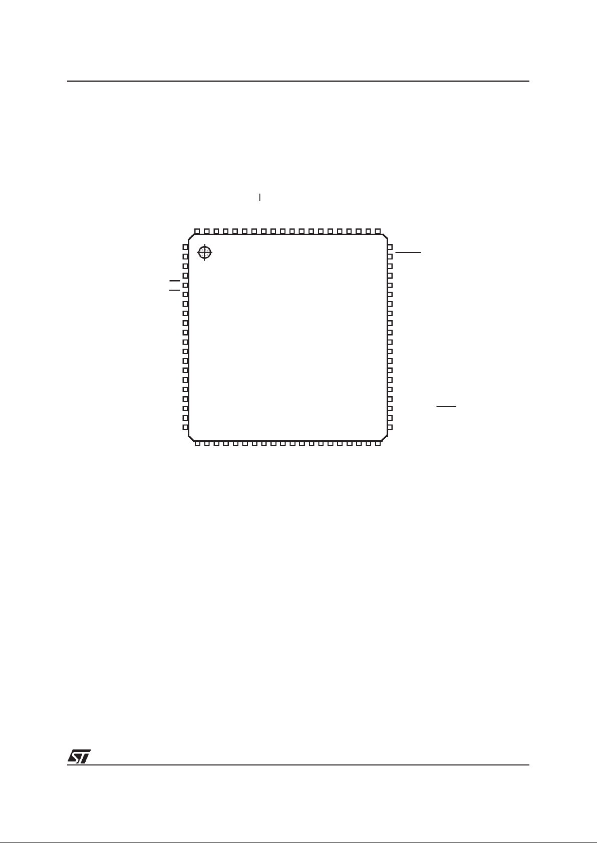
Figure 3. 80-Pin TQFP Pin-out
*EPROM or OTP devices only
ST90158/ST90135
P0.5/AD5
P0.4/AD4
P0.3/AD3
P0.2/AD2
P0.1/AD1
P0.0/AD0
P6.6
P6.5/RW
P6.4
P6.3
P6.2
P6.1
P6.0
P1.7/A15
P1.6/A14
P1.5/A13
P1.4/A12
P1.3/A11
P1.2/A10
P1.1/A9
AD6/P0.6
V
SS
AD7/P0.7
V
DD
AS
DS
V
PP
*
P4.0
P4.1
INTCLK/P4.2
STOUT/P4.3
WDOUT/INT0/P4.4
INT4/P4.5
T0OUTB/INT5/P4.6
T0OUTA/P4.7
P2.0
P2.1
P2.2
P2.3
P2.4
1
20
21
40
41
60
6180
P2.5
P2.6
S1OUT/P9.0
T0OUTB/S1IN/P9.1
TX1CKIN/CLK1OUT/P9.2
S0OUT/RX1CKIN/P9.4
S0IN/P9.5
INT2/SCK/P9.6
INT6/SDO/P9.7
AIN0/RX0CKIN/WDIN/EXTRG/P7.0
AIN1/T0INB/SDI/P7.1
AIN2/CLK0OUT/TX0CKIN/P7.2
AIN3/T0INA/P7.3
AIN4/P7.4
AIN5/P7.5
AIN6/P7.6
AIN7/P7.7
AV
DD
AV
SS
NMI/T3OUTB/P8.7
P1.0/A8
RESET
OSCIN
V
SS
OSCOUT
P5.1/SDI
HW0SW1
P5.3
P5.4/T1OUTA/DCD0
P5.5/T1OUT1/RTS0
P5.6/T3OUTA/DCD1
P5.7/T3OUTB/RTS1/CKAF
V
DD
P8.0/T3INA
P8.1/T1INB
P8.2/INT1/T1OUTA
P8.3/INT3/T1OUTB
P8.4/T1INA/WAIT/WDOUT
P8.5/T3INB
P8.6/INT7/T3OUTA

12/190
ST90158 - GENERAL DESCRIPTION
PIN DESCRIPTION (Cont’d)
Figure 4. 80-Pin PQFP Pin-Out
AD4/P0.4
AD5/P0.5
AD6/P0.6
V
SS
AD7/P0.7
V
DD
AS
DS
V
PP
*
P4.0
P4.1
INTCLK/P4.2
STOUT/P4.3
INT0/WDOUT/P4.4
INT4/P4.5
INT5/T0OUTB/P4.6
T0OUTA/P4.7
P2.0
P2.1
P2.2
P2.3
P2.4
P2.5
P2.6
P0.3/AD3
P0.2/AD2
P0.1/AD1
P0.0/AD0
P6.6
P6.5/RW
P6.4
P6.3
P6.2
P6.1
P6.0
P1.7/A15
P1.6/A14
P1.5/A13
P1.4/A12
P1.3/A11
P1.2/A10
P1.1/A9
P1.0/A8
RESET
OSCIN
V
SS
OSCOUT
P5.1/SDI
HW0SW1
P5.3
P5.4/T1OUTA/DCD0
P5.5/T1OUTB/RTS0
P5.6/T3OUTA/DCD1
P5.7/T3OUTB/RTS1/CK_AF
V
DD
P8.0/T3INA
P8.1/T1INB
P8.2/T1OUTA/INT1
P8.3/T1OUTB/INT3
P8.4/T1INA/WAIT/WDOUT
P8.5/T3INB
P8.6/INT7/T3OUTA
P8.7/NMI/T3OUTB
AV
SS
S1OUT/P9.0
T0OUTB/S1IN/P9.1
TX1CKIN/CLK1OUT/P9.2
S0OUT/RX1CKIN/P9.4
S0IN/P9.5
INT2/SCK/P9.6
INT6/SDO/P9.7
AIN0/RX0CKIN/WDIN/EXTRG/P7.0
AIN1/T0INB/P7.1
AIN2/CLK0OUT/TX0CKIN/P7.2
AIN3/T0INA/P7.3
AIN4/P7.4
AIN5/P7.5
AIN6/P7.6
AIN7/P7.7
AV
DD
1
80
24
40
64
ST90158/ST90135
*EPROM or OTP devices only
9

13/190
ST90158 - GENERAL DESCRIPTION
1.3 I/O PORT PINS
All the ports of the device can be programmed as
Input/Output or in Input mode, compatible with
TTL or CMOS levels (except where Schmitt Trigger is present). Each bit can be programmed individually (Refer to the I/O ports chapter).
TTL/CMOS Input
For all those port bits where no input schmitt trigger is implemented, it is always possible to program the input level as TTL or CMOS compatible
by programming the relevant PxC2.n control bit.
Refer to the sectiontitled “Input/Output Bit Configuration” in the I/O Ports Chapter .
Push-Pull/OD Output
The output buffer can be programmed as pushpull or open-drain: attention must be paid to the
fact thatthe open-drain option correspondsonly to
a disabling of P-channel MOS transistor of the
buffer itself: it is still present and physically connected to thepin. Consequently it isnot possible to
increase the output voltage on the pin over
VDD+0.3 Volt, to avoid direct junctionbiasing.
Table 1. I/O Port Characteristics
Legend: WPU = Weak Pull-Up, OD = Open Drain
Input Output Weak Pull-Up Reset State
Port 0 TTL/CMOS Push-Pull/OD Yes Bidirectional WPU
Port 1 TTL/CMOS Push-Pull/OD Yes Bidirectional WPU
Port 2 TTL/CMOS Push-Pull/OD No Bidirectional
Port 4 Schmitt trigger Push-Pull/OD Yes Bidirectional WPU
Port 5 Schmitt trigger Push-Pull/OD Yes Bidirectional WPU
Port 6 TTL/CMOS Push-Pull/OD No Bidirectional
Port 7 Schmitt trigger Push-Pull/OD Yes Bidirectional WPU
Port 8 Schmitt trigger Push-Pull/OD Yes Bidirectional WPU
Port 9 Schmitt trigger Push-Pull/OD Yes Bidirectional WPU
9

14/190
ST90158 - GENERAL DESCRIPTION
I/O PORT PINS (Cont’d)
How to Configure the I/Oports
To configure the I/O ports, use the information in
Table 1, Table 2 andthe Port BitConfiguration Table in the I/O ports Chapter (See page 92).
Input Note = the hardware characteristics fixed for
each port line in Table1.
– IfInput note = TTL/CMOS, either TTL or CMOS
input level can be selected by software.
– IfInput note = Schmitt trigger, selecting CMOS
or TTL input by software has no effect, the input
will always be Schmitt Trigger.
Alternate Functions (AF) = More than one AF
cannot beassigned to anI/O pin atthe sametime:
An alternate function can be selected as follows.
AF Inputs:
– AF isselected implicitly by enabling the corre-
sponding peripheral. Exceptionto this are A/D
inputs which must beexplicitly selectedas AFby
software.
AF Outputs or Bidirectional Lines:
– In the case of Outputs or I/Os, AF is selected
explicitly by software.
Example 1: SCI data input
AF: S0IN, Port: P9.5, Port Style: Input Schmitt
Trigger.
Write the port configuration bits:
P9C2.5=1
P9C1.5=0
P9C0.5=1
Enable the SCI peripheral by software as de-
scribed in the SCI chapter.
Example 2: SCI data output
AF: S0OUT, Port: P9.4 Output push-pull(configured by software).
Write the port configuration bits:
P9C2.4=0
P9C1.4=1
P9C0.4=1
Example 3: ADC data input
AF: AIN0, Port : P7.0, Input Note: does not apply
to ADC
Write the port configuration bits:
P7C2.0=1
P7C1.0=1
P7C0.0=1
Example 4: External Memory I/O
AF: AD0, Port : P0.0
Write the port configuration bits:
P0C2.0=0
P0C1.0=1
P0C0.0=1
Table 2. I/O Port Description and Alternate Functions
Port
Name
General
Purpose I/O
Pin
No.
Alternate Functions
TQFP
PQFP
P0.0
All ports useable
for general purpose I/O (input,
output or bidirectional)
75 77 AD0 I/O Address/Data bit 0 mux
P0.1 76 78 AD1 I/O Address/Data bit 1 mux
P0.2 77 79 AD2 I/O Address/Data bit 2 mux
P0.3 78 80 AD3 I/O Address/Data bit 3 mux
P0.4 79 1 AD4 I/O Address/Data bit 4 mux
P0.5 80 2 AD5 I/O Address/Data bit 5 mux
P0.6 1 3 AD6 I/O Address/Data bit 6 mux
P0.7 3 5 AD7 I/O Address/Data bit 7 mux
P1.0 60 62 A8 I/O Address bit 8
P1.1 61 63 A9 I/O Address bit 9
P1.2 62 64 A10 I/O Address bit 10
9

15/190
ST90158 - GENERAL DESCRIPTION
P1.3
All ports useable
for general purpose I/O (input,
output or bidirec-
tional)
63 65 A11 I/O Address bit 11
P1.4 64 66 A12 I/O Address bit 12
P1.5 65 67 A13 I/O Address bit 13
P1.6 66 68 A14 I/O Address bit 14
P1.7 67 69 A15 I/O Address bit 15
P2.0 16 18 I/O
P2.1 17 19 I/O
P2.2 18 20 I/O
P2.3 19 21 I/O
P2.4 20 22 I/O
P2.5 21 23 I/O
P2.6 22 24 I/O
P4.0 8 10 I/O
P4.1 9 11 I/O
P4.2 10 12 INTCLK O Internal main Clock
P4.3 11 13 STOUT O Standard Timer Output
P4.4 12 14
INT0 I External Interrupt 0
WDOUT O Watchdog Timeroutput
P4.5 13 15 INT4 I External interrupt 4
P4.6 14 16
INT5 I External Interrupt 5
T0OUTB O MF Timer 0 Output B
1)
P4.7 15 17 T0OUTA O MF Timer 0 Output A
1)
P5.1 55 57 SDI I SPI Serial Data In
P5.3 53 55 I/O
P5.4 52 54
T1OUTA O MF Timer 1 output A
DCD0 I SCI0 Data Carrier Detect
P5.5 51 53
RTS0 O SCI0 Request to Send
T1OUTB O MF Timer 1 output B
P5.6 50 52
T3OUTA O MF Timer 3 output A
DCD1 I SCI1 Data Carrier Detect
1)
P5.7 49 51
RTS1 O SCI1 Request to Send
1)
T3OUTB O MF Timer 3 output B
CK_AF I External Clock Input
P6.0 68 70 I/O
Port
Name
General
Purpose I/O
Pin
No.
Alternate Functions
TQFP
PQFP
9

16/190
ST90158 - GENERAL DESCRIPTION
P6.1
All ports useable
for general purpose I/O (input,
output or bidirec-
tional)
69 71 I/O
P6.2 70 72 I/O
P6.3 71 73 I/O
P6.4 72 74 I/O
P6.5 73 75 R/W O Read/Write
P6.6 74 76 I/O
P7.0 30 32
AIN0 I A/D Analoginput 0
RX0CKIN I SCI0 Receive Clock input
WDIN I T/WD input
EXTRG I A/D External Trigger
P7.1 31 33
AIN1 I A/D Analoginput 1
T0INB I MF Timer 0 input B
1)
SDI I SPI Serial Data In
P7.2 32 34
AIN2 I A/D Analoginput 2
CLK0OUT O SCI0 Byte Sync Clock output
TX0CKIN I SCI0 Transmit Clock input
P7.3 33 35
AIN3 I A/D Analoginput 3
T0INA I MF Timer 0 input A
1)
P7.4 34 36 AIN4 I A/D Analog input 4
P7.5 35 37 AIN5 I A/D Analog input 5
P7.6 36 38 AIN6 I A/D Analog input 6
P7.7 37 39 AIN7 I A/D Analog input 7
P8.0 47 49 T3INA I MF Timer 3input A
P8.1 46 48 T1INB I MF Timer 1input B
P8.2 45 47
INT1 I External interrupt 1
T1OUTA O MF Timer 1 output A
P8.3 44 46
INT3 I External interrupt 3
T1OUTB O MF Timer 1 output B
P8.4 43 45
T1INA I MF Timer 1 input A
WAIT I External Wait input
WDOUT O Watchdog Timeroutput
P8.5 42 44 T3INB I MF Timer 3input B
P8.6 41 43
INT7 I External interrupt 7
T3OUTA O MF Timer 3 output A
P8.7 40 42
NMI I Non-Maskable Interrupt
T3OUTB O MF Timer 3 output B
Port
Name
General
Purpose I/O
Pin
No.
Alternate Functions
TQFP
PQFP
9

17/190
ST90158 - GENERAL DESCRIPTION
Note 1) Not present on ST90135
P9.0
All ports useable
for general purpose I/O (input,
output or bidirec-
tional)
23 25 S1OUT O SCI1 Serial Output
1)
P9.1 24 26
T0OUTB O MF Timer 0 output B
1)
S1IN I SCI1 SerialInput
1)
P9.2 25 27
CLK1OUT O SCI1 Byte Sync Clock output
1)
TX1CKIN I SCI1 Transmit Clock input
1)
P9.4 26 28
S0OUT O SCI0 Serial Output
RX1CKIN O SCI1 Receive Clock input
1)
P9.5 27 29 S0IN I SCI0 Serial Input
P9.6 28 30
INT2 I External interrupt 2
SCK O SPI Serial Clock
P9.7 29 31
INT6 I External interrupt 6
SDO O SPI Serial Data Out
Port
Name
General
Purpose I/O
Pin
No.
Alternate Functions
TQFP
PQFP
9

18/190
ST90158 - DEVICE ARCHITECTURE
2 DEVICE ARCHITECTURE
2.1 CORE ARCHITECTURE
The ST9+ Core or Central Processing Unit (CPU)
features ahighly optimised instructionset, capable
of handling bit, byte (8-bit) and word (16-bit) data,
as well as BCDand Boolean formats; 14 addressing modes are available.
Four independent buses are controlled by the
Core: a 16-bit Memory bus, an 8-bit Register data
bus, an 8-bit Register address bus and a 6-bit Interrupt/DMA bus which connects the interrupt and
DMA controllersin theon-chip peripherals with the
Core.
This multiple bus architecture affords a high degree ofpipeliningand parallel operation, thus making the ST9+ family devices highly efficient, both
for numerical calculation, data handling and with
regard to communication with on-chip peripheral
resources.
2.2 MEMORY SPACES
There are two separate memory spaces:
– The Register File, which comprises 240 8-bit
registers, arranged as 15 groups (Group 0 to E),
each containing sixteen 8-bit registers plus up to
64 pages of 16 registers mapped in Group F,
which hold data and control bits for the on-chip
peripherals and I/Os.
– A single linear memory space accommodating
both program and data. Allof the physically separate memoryareas, including the internal ROM,
internal RAM and external memory are mapped
in this common address space. The total addressable memory space of 4 Mbytes(limited by
the size of on-chip memory and the number of
external address pins) is arranged as 64 segments of 64 Kbytes. Each segment is further
subdivided into four pages of 16 Kbytes, as illustrated in Figure 5. A Memory Management Unit
uses aset of pointer registers to address a22-bit
memory field using 16-bit address-based instructions.
2.2.1 Register File
The Register File consists of(see Figure6):
– 224 general purpose registers (Group 0 to D,
registers R0 to R223)
– 6 system registers in the System Group (Group
E, registers R224 to R239)
– Up to 64 pages, depending on device configura-
tion, each containing up to 16registers, mapped
to Group F (R240 to R255), see Figure 7.
Figure 5. Single Program and Data Memory Address Space
3FFFFFh
3F0000h
3EFFFFh
3E0000h
20FFFFh
02FFFFh
020000h
01FFFFh
010000h
00FFFFh
000000h
8
7
6
5
4
3
2
1
0
63
62
2
1
0
Address 16K Pages 64K Segments
up to 4 Mbytes
Data
Code
255
254
253
252
251
250
249
248
247
9
10
11
21FFFFh
210000h
133
134
135
33
Reserved
132
9

19/190
ST90158 - DEVICE ARCHITECTURE
MEMORY SPACES (Cont’d)
Figure 6. Register Groups Figure 7. Page Pointer for Group F mapping
Figure 8. Addressing the Register File
F
E
D
C
B
A
9
8
7
6
5
4
3
PAGED REGISTERS
SYSTEM REGISTERS
2
1
0
00
15
255
240
239
224
223
VA00432
UP TO
64 PAGES
GENERAL
REGISTERS
PURPOSE
224
PAGE 63
PAGE 5
PAGE 0
PAGE POINTER
R255
R240
R224
R0 VA00433
R234
REGISTERFILE
SYSTEM REGISTERS
GROUP D
GROUP B
GROUP C
(1100)
(0011)
R192
R207
255
240
239
224
223
F
E
D
C
B
A
9
8
7
6
5
4
3
2
1
0
15
VR000118
00
R195
R195
(R0C3h)
PAGED REGISTERS
9

20/190
ST90158 - DEVICE ARCHITECTURE
MEMORY SPACES (Cont’d)
2.2.2 Register Addressing
Register File registers, including Group F paged
registers (but excluding Group D), may be addressed explicitly by means of a decimal, hexadecimal or binary address;thus R231, RE7h and
R11100111b represent the same register (see
Figure 8). Group D registers can only be addressed in Working Register mode.
Note that an upper case “R” is used to denote this
direct addressing mode.
Working Registers
Certain types of instruction require that registers
be specified in the form “rx”, where x is in the
range 0 to 15:these are known as Working Registers.
Note thata lower case“r” isused to denote thisindirect addressing mode.
Two addressing schemes are available: a single
group of 16 working registers, or two separately
mapped groups, each consisting of 8 working registers. These groups may be mapped starting at
any 8 or 16 byte boundary in the register file by
means of dedicated pointer registers. This technique is described in more detail in Section 2.3.3
Register Pointing Techniques, and illustrated in
Figure 9 and in Figure 10.
System Registers
The 16 registers in Group E (R224 to R239) are
System registersand may be addressed usingany
of the register addressing modes. These registers
are described in greater detail in Section 2.3 SYSTEM REGISTERS.
Paged Registers
Up to 64 pages, each containing 16 registers, may
be mapped to Group F. These are addressed using any register addressing mode, in conjunction
with the Page Pointer register,R234, which is one
of the System registers. This register selects the
page to be mapped to Group F and, once set,
does not need to be changedif two or more registers on the same pageare to be addressed in succession.
Therefore ifthe PagePointer, R234, is setto 5, the
instructions:
spp #5
ld R242, r4
will loadthe contents of working registerr4 into the
third register of page5 (R242).
These paged registers holddata and controlinformation relating to the on-chip peripherals, each
peripheral always being associated with the same
pages and registers to ensure code compatibility
between ST9+ devices. The number of these registers therefore depends on the peripherals which
are present in the specific ST9+ family device. In
other words, pages only exist if the relevant peripheral is present.
Table 3. Register File Organization
Hex.
Address
Decimal
Address
Function
Register
File Group
F0-FF 240-255
Paged
Registers
Group F
E0-EF 224-239
System
Registers
Group E
D0-DF 208-223
General
Purpose
Registers
Group D
C0-CF 192-207 Group C
B0-BF 176-191 Group B
A0-AF 160-175 Group A
90-9F 144-159 Group 9
80-8F 128-143 Group 8
70-7F 112-127 Group 7
60-6F 96-111 Group 6
50-5F 80-95 Group 5
40-4F 64-79 Group 4
30-3F 48-63 Group 3
20-2F 32-47 Group 2
10-1F 16-31 Group 1
00-0F 00-15 Group 0
9

21/190
ST90158 - DEVICE ARCHITECTURE
2.3 SYSTEM REGISTERS
The System registers are listed in Table 4. They
are used to perform all the important system settings. Their purpose is described in the following
pages. Refer to the chapter dealing with I/O for a
description of the PORT[5:0] Data registers.
Table 4. System Registers (Group E)
2.3.1 Central Interrupt Control Register
Please referto the ”INTERRUPT”chapter for adetailed description of the ST9 interruptphilosophy.
CENTRAL INTERRUPT CONTROL REGISTER
(CICR)
R230 - Read/Write
Register Group: E (System)
Reset Value: 1000 0111 (87h)
Bit 7 = GCEN:
Global Counter Enable
.
This bit is the Global Counter Enable of the Multifunction Timers. The GCEN bit is ANDed with the
CE bit in theTCR Register (only in devices featuring theMFT Multifunction Timer)in orderto enable
the Timerswhen both bitsare set.This bit is set after the Reset cycle.
Note: If an MFTis not included in the ST9 device,
then this bit hasno effect.
Bit 6 =TLIP:
Top Level Interrupt Pending
.
This bit is set by hardware when a Top Level Interrupt Request is recognized. This bit can also be
set by software to simulate a Top Level Interrupt
Request.
0: No Top Level Interruptpending
1: Top Level Interrupt pending
Bit 5 =TLI:
Top Level Interrupt bit
.
0: Top Level Interrupt isacknowledged depending
on the TLNM bit in the NICR Register.
1: Top Level Interrupt isacknowledged depending
on the IEN andTLNM bitsin theNICR Register
(described in the Interrupt chapter).
Bit 4 =IEN:
Interrupt Enable .
This bit is cleared by interrupt acknowledgement,
and set by interruptreturn (iret). IEN is modified
implicitly byiret, ei and di instructions or by an
interrupt acknowledge cycle. It can also be explicitly written by the user, but only when nointerrupt
is pending. Therefore, the user should execute a
di instruction (or guarantee by other means that
no interrupt request can arrive) before any write
operation to the CICR register.
0: Disable all interruptsexceptTopLevel Interrupt.
1: Enable Interrupts
Bit 3 =IAM:
Interrupt Arbitration Mode
.
This bit is set and clearedby software to select the
arbitration mode.
0: Concurrent Mode
1: Nested Mode.
Bit 2:0 = CPL[2:0]:
Current Priority Level
.
These three bits record the priority level ofthe routine currently running (i.e. the Current PriorityLevel, CPL). The highest priority level is represented
by 000, and the lowest by 111. The CPL bits can
be set by hardware or software and provide the
reference according to which subsequent interrupts are either left pending or are allowedto interrupt the current interrupt service routine.When the
current interrupt is replaced by one of a higher priority, the current priority value is automatically
stored until required in the NICR register.
R239 (EFh) SSPLR
R238 (EEh) SSPHR
R237 (EDh) USPLR
R236 (ECh) USPHR
R235 (EBh) MODE REGISTER
R234 (EAh) PAGE POINTER REGISTER
R233 (E9h) REGISTER POINTER 1
R232 (E8h) REGISTER POINTER 0
R231 (E7h) FLAG REGISTER
R230 (E6h) CENTRAL INT. CNTL REG
R229 (E5h) PORT5 DATA REG.
R228 (E4h) PORT4 DATA REG.
R227 (E3h) PORT3 DATA REG.
R226 (E2h) PORT2 DATA REG.
R225 (E1h) PORT1 DATA REG.
R224 (E0h) PORT0 DATA REG.
70
GCE
N
TLIP TLI IEN IAM CPL2 CPL1 CPL0
9

22/190
ST90158 - DEVICE ARCHITECTURE
SYSTEM REGISTERS (Cont’d)
2.3.2 Flag Register
The Flag Register contains 8 flags which indicate
the CPU status. During an interrupt, theflag register isautomatically stored in the system stack area
and recalled at the end of the interrupt service routine, thus returning the CPU to its original status.
This occurs for all interrupts and, when operating
in nested mode, up to seven versions of the flag
register may be stored.
FLAG REGISTER (FLAGR)
R231- Read/Write
Register Group: E (System)
Reset value: 0000 0000 (00h)
Bit 7 = C:
Carry Flag
.
The carry flag is affected by:
Addition (add, addw, adc, adcw),
Subtraction (sub, subw, sbc, sbcw),
Compare (cp, cpw),
Shift Right Arithmetic (sra, sraw),
Shift Left Arithmetic (sla, slaw),
Swap Nibbles (swap),
Rotate (rrc, rrcw, rlc, rlcw, ror,
rol),
Decimal Adjust (da),
Multiply and Divide (mul, div, divws).
When set, it generally indicates a carry out of the
most significant bit position of the register being
used as an accumulator (bit 7 for byte operations
and bit 15 for word operations).
The carry flag can be set by the Set Carry Flag
(scf) instruction, cleared by the Reset Carry Flag
(rcf) instruction, and complemented by the Complement Carry Flag (ccf) instruction.
Bit 6 = Z:
Zero Flag
. The Zero flag is affected by:
Addition (add, addw, adc, adcw),
Subtraction (sub, subw, sbc, sbcw),
Compare (cp, cpw),
Shift Right Arithmetic (sra, sraw),
Shift Left Arithmetic (sla, slaw),
Swap Nibbles (swap),
Rotate (rrc, rrcw, rlc, rlcw, ror,
rol),
Decimal Adjust (da),
Multiply and Divide (mul, div, divws),
Logical (and, andw, or, orw, xor,
xorw, cpl),
Increment and Decrement (inc, incw, dec,
decw),
Test (tm, tmw, tcm, tcmw, btset).
Inmostcases,theZeroflagissetwhenthecontents
of the register being used as an accumulator become zero, following one of the above operations.
Bit 5 =S:
Sign Flag
.
The Sign flag is affected by the same instructions
as the Zero flag.
The Sign flag is set when bit 7 (for a byte operation) or bit 15 (for a word operation) of the register
used as an accumulator is one.
Bit 4 =V:
Overflow Flag
.
The Overflow flag is affected by the same instructions as the Zero and Sign flags.
When set, the Overflowflag indicates that a two’scomplement number, in a result register, is in error, since it has exceeded the largest (or is less
than the smallest), number that can be represented in two’s-complement notation.
Bit 3 =DA:
Decimal Adjust Flag
.
The DA flag is used for BCDarithmetic. Since the
algorithm for correcting BCD operations is different for addition and subtraction, this flag is used to
specify which type of instruction was executed
last, so that the subsequent Decimal Adjust (da)
operation can perform its function correctly. The
DA flag cannot normally be used as a test condition by the programmer.
Bit 2 =H:
Half Carry Flag.
The H flag indicates a carry out of(or a borrow into) bit 3, as the result of adding or subtracting two
8-bit bytes, each representing two BCD digits. The
H flag is used by the Decimal Adjust (da) instruction to convert the binary result of a previous addition orsubtraction into the correct BCDresult. Like
the DA flag, this flag is not normally accessed by
the user.
Bit 1 = Reserved bit (must be 0).
Bit 0 =DP:
Data/Program Memory Flag
.
This bit indicates the memory area addressed. Its
value is affected by the Set Data Memory (sdm)
and Set Program Memory (spm) instructions. Re-
fer tothe Memory Management Unit for further details.
70
C Z S V DA H - DP
9

23/190
ST90158 - DEVICE ARCHITECTURE
SYSTEM REGISTERS (Cont’d)
If the bit is set, data is accessed using the Data
Pointers (DPRs registers), otherwise it is pointed
to by the Code Pointer (CSR register); therefore,
the user initialization routine must include a Sdm
instruction. Note that code is always pointed to by
the Code Pointer (CSR).
Note: In the ST9+, the DP flag is only for compatibility with software developed for the first generation of ST9 devices. With the single memory addressing space, its use is now redundant. It must
be kept to 1 with a Sdm instruction at the beginning
of the program to ensure anormal use of the different memory pointers.
2.3.3 Register Pointing Techniques
Two registers within the System register group,
are usedas pointers to theworking registers. Register Pointer0 (R232) maybe used on its ownas a
single pointer to a 16-register working space, or in
conjunction with Register Pointer 1 (R233), to
point to two separate 8-register spaces.
For thepurpose of register pointing,the 16 register
groups of the register file are subdivided into 32 8register blocks. The values specified with the Set
Register Pointer instructions refer to the blocks to
be pointedto in twin 8-register mode, or tothe lower 8-register block location in single 16-register
mode.
The Set Register Pointer instructions srp, srp0
and srp1 automatically inform the CPU whether
the Register File is to operate in single 16-register
mode or in twin 8-register mode. The srp instruction selects the single 16-register groupmode and
specifies the location of the lower 8-register block,
while thesrp0 and srp1 instructions automatically select the twin 8-register group mode and specify the locations of each 8-register block.
There is no limitation on the order or position of
these register groups, other than that they must
start on an 8-register boundary in twin 8-register
mode, or on a 16-register boundary in single 16register mode.
The block number should always be an even
number in single 16-register mode. The 16-register group will always start at the block whose
number is the nearest even number equal to or
lower than the block number specified in the srp
instruction. Avoid using odd block numbers, since
this can be confusing if twin mode is subsequently
selected.
Thus:
srp #3 will be interpreted as srp #2 and will al-
low using R16 ..R31 as r0 .. r15.
In single 16-register mode, the working registers
are referred to as r0 to r15. In twin 8-register
mode, registers r0 tor7 are in the block pointed
to by RP0 (by means of the srp0 instruction),
while registers r8 to r15 are in the block pointed
to by RP1 (bymeans of the srp1 instruction).
Caution:
Group D registers can only be accessed
as working registers using the Register Pointers,
or bymeans of the StackPointers. Theycannot be
addressed explicitly in the form “Rxxx”.
9

24/190
ST90158 - DEVICE ARCHITECTURE
SYSTEM REGISTERS (Cont’d)
POINTER 0 REGISTER (RP0)
R232 - Read/Write
Register Group: E (System)
Reset Value: xxxx xx00 (xxh)
Bit 7:3 = RG[4:0]:
Register Group number.
These bits contain the number (in the range 0 to
31) of the register block specified in the srp0 or
srp instructions. In single 16-register mode the
number indicates the lower of the two 8-register
blocks to which the16 working registers are to be
mapped, whilein twin 8-register mode it indicates
the 8-register block to which r0 to r7 are to be
mapped.
Bit 2 = RPS:
Register Pointer Selector
.
This bitis set bythe instructions srp0 andsrp1 to
indicate that the twin register pointing mode is selected. The bit is reset by the srp instruction to indicate that the single register pointing mode is selected.
0: Single register pointing mode
1: Twin register pointing mode
Bit 1:0: Reserved. Forced by hardware to zero.
POINTER 1 REGISTER (RP1)
R233 - Read/Write
Register Group: E (System)
Reset Value: xxxx xx00(xxh)
This register is only used inthe twin register pointing mode. When using the single register pointing
mode, or when using only one of the twin register
groups, the RP1 register must be considered as
RESERVED and may NOT be used as a general
purpose register.
Bit 7:3 = RG[4:0]:
Register Group number.
These
bits contain the number (in the range 0 to 31) of
the 8-register block specified inthe srp1 instruction, to which r8 to r15 are to be mapped.
Bit 2 =RPS:
Register Pointer Selector
.
This bit isset by thesrp0 and srp1 instructions to
indicate that the twin register pointing mode is selected. Thebit is reset by the srp instruction to indicate that the single register pointing mode is selected.
0: Single register pointing mode
1: Twin register pointing mode
Bit 1:0: Reserved. Forced by hardware to zero.
70
RG4 RG3 RG2 RG1 RG0 RPS 0 0
70
RG4 RG3 RG2 RG1 RG0 RPS 0 0
9
25/190
ST90158 - DEVICE ARCHITECTURE
SYSTEM REGISTERS (Cont’d)
Figure 9. Pointing to a single group of 16
registers
Figure 10.Pointing to two groups of 8 registers
31
30
29
28
27
26
25
9
8
7
6
5
4
3
2
1
0
F
E
D
4
3
2
1
0
BLOCK
NUMBER
REGISTER
GROUP
REGISTER
FILE
REGISTER
POINTER 0
srp #2
set by:
instruction
points to:
GROUP 1
addressed by
BLOCK 2
r15
r0
31
30
29
28
27
26
25
9
8
7
6
5
4
3
2
1
0
F
E
D
4
3
2
1
0
BLOCK
NUMBER
REGISTER
GROUP
REGISTER
FILE
REGISTER
POINTER 0
srp0 #2
set by:
instructions
point to:
GROUP 1
addressed by
BLOCK 2
&
REGISTER
POINTER 1
srp1 #7
&
GROUP 3
addressed by
BLOCK 7
r7
r0
r15
r8
9

26/190
ST90158 - DEVICE ARCHITECTURE
SYSTEM REGISTERS (Cont’d)
2.3.4 Paged Registers
Up to 64 pages, each containing 16 registers, may
be mapped to Group F. These paged registers
hold data and control information relating to the
on-chip peripherals, each peripheral always being
associated with the same pages and registers to
ensure code compatibility between ST9+ devices.
The number of these registers dependson theperipherals presentin the specific ST9 device. In other words, pagesonly exist if the relevant peripheral is present.
The paged registers are addressed using thenormal register addressingmodes, inconjunction with
the Page Pointer register, R234, which is one of
the System registers. This register selects the
page to be mapped to Group F and, once set,
does not need to be changedif two or more registers on the same pageare to be addressed in succession.
Thus the instructions:
spp #5
ld R242, r4
will load the contents of working register r4 into the
third register of page 5 (R242).
Warning:
During an interrupt, the PPR register is
not saved automatically in the stack. If needed, it
should be saved/restored by the user within theinterrupt routine.
PAGE POINTER REGISTER (PPR)
R234 - Read/Write
Register Group: E (System)
Reset value: xxxx xx00 (xxh)
Bit 7:2 = PP[5:0]:
Page Pointer
.
These bits contain the number (in the range 0 to
63) of the page specified in the spp instruction.
Once the page pointer has been set, there is no
need to refresh it unless a different page is required.
Bit 1:0: Reserved. Forced by hardware to 0.
2.3.5 Mode Register
The Mode Register allows control of the following
operating parameters:
– Selectionof internalor external Systemand User
Stack areas,
– Management of the clock frequency,
– Enabling of Bus request and Wait signals when
interfacing to external memory.
MODE REGISTER (MODER)
R235 - Read/Write
Register Group: E (System)
Reset value: 1110 0000 (E0h)
Bit 7 =SSP:
System Stack Pointer
.
This bit selects an internal or external System
Stack area.
0: External system stack area, in memory space.
1: Internal system stack area, in the Register File
(reset state).
Bit 6 =USP:
User Stack Pointer
.
This bit selects an internal or external User Stack
area.
0: External user stack area, in memory space.
1: Internaluser stack area,in the Register File (re-
set state).
Bit 5 =DIV2:
OSCIN Clock Divided by 2
.
This bit controls the divide-by-2 circuit operating
on OSCIN.
0: Clock divided by 1
1: Clock divided by 2
Bit 4:2 = PRS[2:0]:
CPUCLK Prescaler
.
These bitsload the prescaler division factor for the
internal clock (INTCLK). The prescaler factor selects theinternal clock frequency, which can be divided by a factor from 1 to 8. Refer to the Reset
and Clock Control chapterfor further information.
Bit 1 =BRQEN:
Bus Request Enable
.
0: External Memory Bus Request disabled
1: External Memory Bus Request enabled on the
BREQ pin (where available).
Bit 0 =HIMP:
High Impedance Enable
.
When any of Ports 0, 1, 2 or 6 depending on device configuration, are programmed as Address
and Data lines to interface external Memory, these
lines and the Memory interface control lines (AS,
70
PP5 PP4 PP3 PP2 PP1 PP0 0 0
70
SSP USP DIV2 PRS2 PRS1 PRS0 BRQEN HIMP
9

27/190
ST90158 - DEVICE ARCHITECTURE
SYSTEM REGISTERS (Cont’d)
DS, R/W) can be forced into the High Impedance
state bysetting the HIMP bit. When this bitis reset,
it has no effect.
Setting the HIMPbit is recommended fornoise reduction when only internal Memory is used.
If Port 1 and/or 2 are declared as an address AND
as an I/O port (for example: P10... P14 = Address,
and P15... P17 = I/O), the HIMP bit has no effect
on the I/O lines.
2.3.6 Stack Pointers
Two separate, double-register stack pointers are
available: the System Stack Pointer and the User
Stack Pointer, both of which can address registers
or memory.
The stack pointers point to the “bottom” of the
stacks which are filled using the push commands
and emptied using the pop commands. The stack
pointer is automatically pre-decremented when
data is “pushed” in and post-incremented when
data is “popped” out.
The push and pop commands usedto manage the
System Stack may be addressed to the User
Stack by adding the suffix “u”. To use a stackinstruction for a word, the suffix “w” is added. These
suffixes may be combined.
When bytes (or words) are “popped” out from a
stack, the contents of the stack locations are unchanged until fresh data is loaded. Thus, when
data is “popped” from a stack area, the stack contents remain unchanged.
Note: Instructions such as: pushuw RR236 or
pushw RR238, as well as the corresponding
pop instructions (where R236 & R237, and R238
& R239 are themselves theuser and systemstack
pointers respectively), mustnot be used, since the
pointer values are themselves automatically
changed by the push or pop instruction, thus corrupting their value.
System Stack
The System Stack is used for the temporary storage of system and/or control data, such as the
Flag register and the Program counter.
The following automatically push data onto the
System Stack:
– Interrupts
When entering an interrupt, the PC and the Flag
Register are pushed onto the System Stack. If the
ENCSR bit in the EMR2 register is set, then the
Code Segment Register is also pushed onto the
System Stack.
– Subroutine Calls
When a call instruction is executed, only the PC
is pushed onto stack, whereas when a calls instruction (call segment) is executed, both the PC
and the Code Segment Register are pushed onto
the System Stack.
– Link Instruction
The link or linku instructions create a C lan-
guage stack frame of user-defined length in the
System or User Stack.
All of the above conditions are associated with
their counterparts, such as return instructions,
which pop the stored data items off the stack.
User Stack
The User Stack provides a totally user-controlled
stacking area.
The User Stack Pointer consists of two registers,
R236 and R237, whichare both used for addressing a stack in memory. When stacking in the Register File, the User Stack Pointer High Register,
R236, becomes redundant but must be considered as reserved.
Stack Pointers
Both System and User stacks are pointed to by
double-byte stack pointers. Stacks may be set up
in RAM or in the Register File. Only the lower byte
will be required if the stack is in the Register File.
The upper byte must then be considered as reserved and mustnot be used asa general purpose
register.
The stack pointer registers are located in the System Group ofthe Register File, thisis illustratedin
Table 4.
Stack location
Care is necessary whenmanaging stacks as there
is no limit to stack sizes apart from the bottom of
any address space in which the stack is placed.
Consequently programmers are advised to use a
stack pointer value as high as possible, particularly when using the RegisterFile as astacking area.
Group D is a good location for a stack in the Register File,since it is the highest availablearea. The
stacks may be located anywhere in the first 14
groups of the Register File (internal stacks) or in
RAM (external stacks).
Note. Stacks must not be located in the Paged
Register Group or in theSystem Register Group.
9
28/190
ST90158 - DEVICE ARCHITECTURE
SYSTEM REGISTERS (Cont’d)
USER STACK POINTER HIGH REGISTER
(USPHR)
R236 - Read/Write
Register Group: E (System)
Reset value: undefined
USER STACK POINTER LOW REGISTER
(USPLR)
R237 - Read/Write
Register Group: E (System)
Reset value: undefined
Figure 11. Internal Stack Mode
SYSTEM STACK POINTER HIGH REGISTER
(SSPHR)
R238 - Read/Write
Register Group: E (System)
Reset value: undefined
SYSTEM STACK POINTER LOW REGISTER
(SSPLR)
R239 - Read/Write
Register Group: E (System)
Reset value: undefined
Figure 12. External Stack Mode
70
USP15USP14USP13USP12USP11USP1
0
USP9 USP8
70
USP7 USP6 USP5 USP4 USP3 USP2 USP1 USP0
F
E
D
4
3
2
1
0
REGISTER
FILE
STACKPOINTER (LOW)
points to:
STACK
70
SSP15SSP14SSP13SSP12SSP11SSP1
0
SSP9 SSP8
70
SSP7 SSP6 SSP5 SSP4 SSP3 SSP2 SSP1 SSP0
F
E
D
4
3
2
1
0
REGISTER
FILE
STACK POINTER (LOW)
point to:
STACK
MEMORY
STACKPOINTER (HIGH)
&
9

29/190
ST90158 - DEVICE ARCHITECTURE
2.4 MEMORY ORGANIZATION
Code and data are accessed within thesame linear address space. All of the physically separate
memory areas, including the internal ROM, internal RAM and external memory are mapped in a
common address space.
The ST9+ provides a total addressable memory
space of 4 Mbytes. This address space is arranged as 64 segments of 64 Kbytes; each segment isagain subdividedinto four 16Kbyte pages.
The mapping of the various memory areas (internal RAM or ROM, external memory) differs from
device to device. Each 64-Kbyte physical memory
segment is mapped either internally or externally;
if the memory is internal and smaller than 64
Kbytes, the remaining locations in the 64-Kbyte
segment are not used (reserved).
Refer to the Register and Memory Map Chapter
for more details on the memory map.
9

30/190
ST90158 - DEVICE ARCHITECTURE
2.5 MEMORY MANAGEMENT UNIT
The CPU Core includes a Memory Management
Unit (MMU) which must be programmed to perform memory accesses (even if external memory
is not used).
The MMU is controlled by 7 registers and 2 bits
(ENCSR and DPRREM) present in EMR2, which
may be written and read by the user program.
These registers are mapped within group F, Page
21 of the Register File. The 7 registers may be
sub-divided into 2main groups: a first group of four
8-bit registers (DPR[3:0]), and a second group of
three 6-bitregisters (CSR,ISR, and DMASR). The
first group is used to extend the address during
Data Memory access (DPR[3:0]). The second is
used to manage Program and Data Memory accesses during Code execution (CSR), Interrupts
Service Routines (ISR or CSR), and DMA transfers (DMASR or ISR).
Figure 13. Page 21 Registers
DMASR
ISR
EMR2
EMR1
CSR
DPR3
DPR2
DPR1
DPR0
R255
R254
R253
R252
R251
R250
R249
R248
R247
R246
R245
R244
R243
R242
R241
R240
FFh
FEh
FDh
FCh
FBh
FAh
F9h
F8h
F7h
F6h
F5h
F4h
F3h
F2h
F1h
F0h
MMU
EM
Page 21
MMU
MMU
Bit DPRREM=0
SSPLR
SSPHR
USPLR
USPHR
MODER
PPR
RP1
RP0
FLAGR
CICR
P5DR
P4DR
P3DR
P2DR
P1DR
P0DR
DMASR
ISR
EMR2
EMR1
CSR
DPR3
DPR2
1
DPR0
Bit DPRREM=1
SSPLR
SSPHR
USPLR
USPHR
MODER
PPR
RP1
RP0
FLAGR
CICR
P5DR
P4DR
P3DR
P2DR
P1DR
P0DR
DMASR
ISR
EMR2
EMR1
CSR
DPR3
DPR2
DPR1
DPR0
Relocation of P[3:0] and DPR[3:0] Registers
(default setting)
9

31/190
ST90158 - DEVICE ARCHITECTURE
2.6 ADDRESS SPACE EXTENSION
To manage 4 Mbytes of addressing space it is
necessary to have 22 address bits. The MMU
adds 6 bits tothe usual 16-bit address, thus translating a 16-bit virtualaddress into a 22-bit physical
address. There are 2 different ways to do this depending on the memory involved and onthe operation being performed.
2.6.1 Addressing 16-Kbyte Pages
This extension mode is implicitly used to address
Data memoryspace if noDMA isbeing performed.
The Data memory space is divided into 4 pages of
16 Kbytes. Each one of the four 8-bit registers
(DPR[3:0], Data Page Registers) selects a different 16-Kbyte page. The DPR registers allow access to the entire memory space which contains
256 pages of 16 Kbytes.
Data pagingis performed byextending the14 LSB
of the 16-bit address with the contents of a DPR
register. The two MSBs of the 16-bit address are
interpreted asthe identificationnumber ofthe DPR
register to be used. Therefore, the DPR registers
are involved in the following virtual address ranges:
DPR0: from 0000h to 3FFFh;
DPR1: from 4000h to 7FFFh;
DPR2: from 8000h to BFFFh;
DPR3: from C000h to FFFFh.
The contents of the selected DPR register specify
one of the 256 possible data memory pages. This
8-bit data page number, in addition to theremaining 14-bit page offset address forms the physical
22-bit address (see Figure 14).
A DPRregister cannotbe modified via an addressing modethat uses thesame DPR register. For instance, theinstruction “POPW DPR0” is legal only
if the stack is kept either in the register file or in a
memory location above 8000h, where DPR2 and
DPR3 are used. Otherwise, since DPR0 and
DPR1 are modified by the instruction, unpredictable behaviour could result.
Figure 14. Addressing via DPR[3:0]
DPR0 DPR1 DPR2 DPR3
00
01 10 11
16-bit virtual address
22-bit physical address
8 bits
MMU registers
2
M
SB
14 LSB
9

32/190
ST90158 - DEVICE ARCHITECTURE
ADDRESS SPACE EXTENSION (Cont’d)
2.6.2 Addressing 64-Kbyte Segments
This extension mode is used to address Data
memory space during a DMA and Program memory spaceduring any code execution (normalcode
and interrupt routines).
Three registers are used: CSR, ISR, and DMASR.
The 6-bit contents of one of the registers CSR,
ISR, or DMASR define one out of 64 Memory segments of 64 Kbytes within the 4 Mbytes address
space. The register contents represent the 6
MSBs of the memory address, whereas the 16
LSBs of the address (intra-segment address) are
given by thevirtual 16-bit address (see Figure 15).
2.7 MMU REGISTERS
The MMU uses 7 registers mapped into Group F,
Page 21 of the Register File and 2 bits of the
EMR2 register.
Most of these registers do not have a default value
after reset.
2.7.1 DPR[3:0]: Data Page Registers
The DPR[3:0]registers allow access to the entire 4
Mbyte memory space composed of 256 pages of
16 Kbytes.
2.7.1.1 Data Page Register Relocation
If these registers are to be used frequently, they
may be relocated in register group E, by programming bit 5of the EMR2-R246 register in page 21. If
this bit is set, the DPR[3:0] registers are located at
R224-227 in place of the Port 0-3Data Registers,
which are re-mapped to the default DPR’s locations: R240-243 page 21.
Data Page Register relocation is illustrated in Figure 13.
Figure 15. Addressing via CSR, ISR, and DMASR
Fetching program
Data Memory
Fetching interrupt
instruction
accessed in DMA
instruction or DMA
access to Program
Memory
16-bit virtual address
22-bit physicaladdress
6 bits
MMU registers
CSR
ISR
DMASR
123
1
2
3
9

33/190
ST90158 - DEVICE ARCHITECTURE
MMU REGISTERS (Cont’d)
DATA PAGE REGISTER 0 (DPR0)
R240 - Read/Write
Register Page: 21
Reset value: undefined
This register is relocated to R224if EMR2.5 is set.
Bit 7:0 = DPR0_[7:0]: These bits define the 16Kbyte Data Memory page number. They are used
as themostsignificant addressbits(A21-14) to extend the address during a Data Memory access.
The DPR0 register is used when addressing the
virtual address range 0000h-3FFFh.
DATA PAGE REGISTER 1 (DPR1)
R241 - Read/Write
Register Page: 21
Reset value: undefined
This register is relocated to R225if EMR2.5 is set.
Bit 7:0 = DPR1_[7:0]: These bits define the 16Kbyte Data Memory page number. They are used
as themostsignificant addressbits(A21-14) to extend the address during a Data Memory access.
The DPR1 register is used when addressing the
virtual address range 4000h-7FFFh.
DATA PAGE REGISTER 2 (DPR2)
R242 - Read/Write
Register Page: 21
Reset value: undefined
This register is relocated to R226if EMR2.5 is set.
Bit 7:0 = DPR2_[7:0]: These bits define the 16-
Kbyte Data memory page. They are used as the
most significant address bits (A21-14) to extend
the address during a Data memory access. The
DPR2 register is involved when the virtual address
is in the range 8000h-BFFFh.
DATA PAGE REGISTER 3 (DPR3)
R243 - Read/Write
Register Page: 21
Reset value: undefined
This register is relocated to R227if EMR2.5 is set.
Bit 7:0 = DPR3_[7:0]: These bits define the 16-
Kbyte Data memory page. They are used as the
most significant address bits (A21-14) to extend
the address during a Data memory access. The
DPR3 register is involved when the virtual address
is in the range C000h-FFFFh.
70
DPR0_7DPR0_6DPR0_5DPR0_4DPR0_3DPR0_2DPR0_1DPR0
_0
70
DPR1_7DPR1_6DPR1_5DPR1_4DPR1_3DPR1_2DPR1_1DPR1
_0
70
DPR2_7DPR2_6DPR2_5DPR2_4DPR2_3DPR2_2DPR2_1DPR2
_0
70
DPR3_7DPR3_6DPR3_5DPR3_4DPR3_3DPR3_2DPR3_1DPR3
_0
9

34/190
ST90158 - DEVICE ARCHITECTURE
MMU REGISTERS (Cont’d)
2.7.2 CSR: Code Segment Register
This register selects the 64-Kbyte code segment
being used at run-time to access instructions. It
can also be used toaccess data if the spm instruction has been executed (orldpp, ldpd, lddp).
Only the 6 LSBs of the CSR register are implemented, and bits 6 and 7 are reserved. The CSR
register allowsaccess to the entirememory space,
divided into 64 segmentsof 64 Kbytes.
To generate the 22-bit Program memory address,
the contents of theCSR register is directly used as
the 6 MSBs, and the 16-bit virtual address as the
16 LSBs.
Note: The CSR register should only be read and
not written for data operations (there are some exceptions which are documented in the following
paragraph). It is, however, modified either directly
by means of the jps and calls instructions, or
indirectly via the stack, by means of the rets instruction.
CODE SEGMENT REGISTER (CSR)
R244 - Read/Write
Register Page: 21
Reset value: 0000 0000 (00h)
Bit 7:6 = Reserved, keep in resetstate.
Bit 5:0 = CSR_[5:0]: These bits define the 64Kbyte memory segment (among 64) which contains the code being executed. These bits are
used asthe most significant address bits (A21-16).
2.7.3 ISR: Interrupt Segment Register
INTERRUPT SEGMENT REGISTER (ISR)
R248 - Read/Write
Register Page: 21
Reset value: undefined
ISR and ENCSR bit (EMR2 register) are also described inthe chapter relating to Interrupts, please
refer to this description forfurther details.
Bit 7:6 = Reserved, keepin reset state.
Bit 5:0= ISR_[5:0]: These bits define the 64-Kbyte
memory segment (among 64) which contains the
interrupt vector table and the code for interrupt
service routines and DMA transfers (when the PS
bit of the DAPR register is reset). These bits are
used as themost significant addressbits(A21-16).
The ISR is used to extend the address space in
two cases:
– Whenever an interrupt occurs:ISR points to the
64-Kbyte memory segment containing the interrupt vectortable andthe interrupt serviceroutine
code. See also the Interrupts chapter.
– DuringDMAtransactions betweenthe peripheral
and memory when the PS bit ofthe DAPR register is reset : ISR points to the64 K-byte Memory
segment that will be involved in the DMA transaction.
2.7.4 DMASR: DMA Segment Register
DMA SEGMENT REGISTER (DMASR)
R249 - Read/Write
Register Page: 21
Reset value: undefined
Bit 7:6 = Reserved, keepin reset state.
Bit 5:0 = DMASR_[5:0]: Thesebits define the 64Kbyte Memory segment (among 64) used when a
DMA transactionis performed betweenthe peripheral’s data register and Memory, with the PS bit of
the DAPR register set. These bits are used as the
most significant addressbits (A21-16). If the PS bit
is reset, the ISR register is used to extend the address.
70
00
CSR_5CSR_4CSR_3CSR_2CSR_1CSR_
0
70
0 0 ISR_5 ISR_4 ISR_3 ISR_2 ISR_1 ISR_0
70
00
DMA
SR_5
DMA
SR_4
DMA
SR_3
DMA
SR_2
DMA
SR_1
DMA
SR_0
9

35/190
ST90158 - DEVICE ARCHITECTURE
MMU REGISTERS (Cont’d)
Figure 16. Memory Addressing Scheme (example)
3FFFFFh
294000h
240000h
23FFFFh
20C000h
200000h
1FFFFFh
040000h
03FFFFh
030000h
020000h
010000h
00C000h
000000h
DMASR
ISR
CSR
DPR3
DPR2
DPR1
DPR0
4M bytes
16K
16K
16K
64K
64K
64K
16K
9

36/190
ST90158 - DEVICE ARCHITECTURE
2.8 MMU USAGE
2.8.1 Normal Program Execution
Program memory is organized as a set of 64Kbyte segments. The program can span as many
segments as needed, but a procedure cannot
stretch across segment boundaries. jps, calls
and rets instructions, which automatically modify
the CSR, must be used to jump across segment
boundaries. Writing to the CSR is forbidden during
normal program execution because it is not synchronized with the opcode fetch. This could result
in fetching the first byte of an instruction from one
memory segmentandthe second byte from another. Writing tothe CSR isallowed when it is not being used, i.e during an interrupt service routine if
ENCSR is reset.
Note that a routine must always be called in the
same way, i.e. either always with call or always
with calls, depending on whether the routine
ends withret or rets. This means that ifthe routine is written without prior knowledge of the location of other routines which call it, and all the program code does not fit into a single 64-Kbyte segment, then calls/rets should be used.
In typicalmicrocontroller applications, less than 64
Kbytes of RAM are used, so the four Data space
pages are normally sufficient, and no change of
DPR[3:0] is needed during Program execution. It
may be useful however to map part of the ROM
into the data space if it contains strings, tables, bit
maps, etc.
If there is to be frequent use of paging, the user
can set bit 5 (DPRREM) in register R246 (EMR2)
of Page 21. This swaps the location of registers
DPR[3:0] with that of the data registers of Ports 0-
3. In this way, DPR registers can be accessed
without the need to save/set/restore the Page
Pointer Register. Port registers are therefore
moved topage 21. Applicationsthat require a lot of
paging typically use more than 64 Kbytesof external memory, and as ports 0, 1 and2 are required
to address it, their data registers are unused.
2.8.2 Interrupts
The ISR register has been created so that the interrupt routines may be found by means of the
same vector table even after a segment jump/call.
When an interrupt occurs, the CPU behaves in
one of2 ways, depending on the value ofthe ENCSR bit in the EMR2 register(R246 on Page 21).
If this bit is reset (default condition), the CPU
works in original ST9 compatibility mode. For the
duration of the interrupt service routine, the ISR is
used instead of the CSR, and the interrupt stack
frame is kept exactly as in the original ST9 (only
the PC and flags are pushed). This avoids the
need to save the CSR on the stack in the case of
an interrupt, ensuring a fast interrupt response
time. The drawback is that it is not possible foran
interrupt service routine to perform segment
calls/jps: these instructions would update the
CSR, which, in this case, is not used (ISR is used
instead). The code size of all interrupt service routines is thus limited to64 Kbytes.
If, instead, bit 6 of the EMR2 register is set, the
ISR is used only to point to the interrupt vectortable andto initialize the CSR at the beginning of the
interrupt service routine: the old CSR is pushed
onto the stack together with the PC and the flags,
and then the CSR is loaded with the ISR. In this
case, an iret will also restore the CSR from the
stack. This approach letsinterrupt service routines
access the whole 4-Mbyte address space. The
drawback is that the interrupt response time is
slightly increased, because of the need to also
save the CSR onthe stack. Compatibility with the
original ST9 is also lost in this case, because the
interrupt stack frame is different; this difference,
however, wouldnot be noticeable for a vast majority of programs.
Data memorymapping is independent ofthe value
of bit 6 of the EMR2 register, and remains the
same as for normal code execution: the stack is
the same as that used by the main program, as in
the ST9. If the interrupt service routine needs to
access additional Data memory, it must save one
(or more) of the DPRs, load it with the needed
memory page and restore it before completion.
2.8.3 DMA
Depending on the PS bit in the DAPR register (see
DMA chapter) DMA uses either the ISR or the
DMASR for memory accesses: this guarantees
that a DMA will always find its memory segment(s), no matter what segment changes the application has performed. Unlike interrupts, DMA
transactions cannot save/restore paging registers,
so a dedicated segment register (DMASR) has
been created.Having only one register of this kind
means that all DMA accesses should be programmed in one of the two following segments:
the one pointed to by the ISR (when the PS bit of
the DAPR register is reset), and the one referenced by the DMASR (when thePS bit is set).
9

37/190
ST90158 - REGISTER AND MEMORY MAP
3 REGISTER AND MEMORY MAP
3.1 MEMORY CONFIGURATION
The Program memory space of the ST90135/158,
0/16/24/32/48/64/K bytes of directly addressable
on-chip memory, is fully available to the user.
The first 256 memory locations from address 0 to
FFh hold the ResetVector, the Top-Level (Pseudo
Non-Maskable) interrupt, the Divide by Zero Trap
Routine vector and, optionally, the interrupt vector
table for use with the on-chip peripherals and the
external interrupt sources. Apart from this case no
other part of the Program memory has a predetermined function except segment 21h which is reserved for use by STMicroelectronics.
3.2 EPROM PROGRAMMING
The 65536 bytes of EPROM memory of the
ST90E158 may be programmed by using the
EPROM Programming Boards (EPB) organg programmers available from STMicroelectronics.
EPROM Erasing
The EPROM of the windowed package of the
ST90E158 maybe erased by exposure toUltra-Violet light.
The erasure characteristic of the ST90E158 is
such that erasure begins when the memory is exposed to light with a wavelengths shorter than approximately 4000Å.It shouldbe notedthat sunlight
and some types of fluorescent lamps have wavelengths in the range 3000-4000Å. It isthus recommended that the window of theST90E158 packages becovered by an opaquelabel to prevent unintentional erasure problems when testing the application in such an environment.
The recommended erasure procedure of the
EPROM is the exposure to short wave ultraviolet
light which have a wave-length 2537Å. The integrated dose (i.e.U.V. intensity xexposure time) for
erasure should be a minimum of 15W-sec/cm2.
The erasure time with this dosage is approximately 30 minutes using an ultraviolet lamp with
12000mW/cm2 power rating. The ST90E158
should be placed within 2.5cm (1 inch) of the lamp
tubes during erasure.
Table 5. First 6 Bytes of Program Space
0 Address high of Power on Reset routine
1 Address low of Power on Reset routine
2 Address high of Divide by zero trap Subroutine
3 Address low of Divide by zero trap Subroutine
4 Address high of Top Level Interrupt routine
5 Address low of Top Level Interrupt routine
9

38/190
ST90158 - REGISTER AND MEMORY MAP
Figure 17. Interrupt Vector Table
USER ISR
PROGRAM MEMORY
POWER-ON RESET
DIVIDE-BY-ZERO
TOP LEVEL INT.
LO
LO
LO
HI
HI
HI
000000h
USER MAIN PROGRAM
USER TOP LEVEL ISR
USER DIVIDE-BY-ZERO ISR
0000FFh
VECTOR
TABLE
ISR ADDRESS
EVEN
ODD
INT. VECTOR REGISTER
LO
HI
REGISTERFILE
R240
R239
F PAGE REGISTERS
000002h
000004h
9
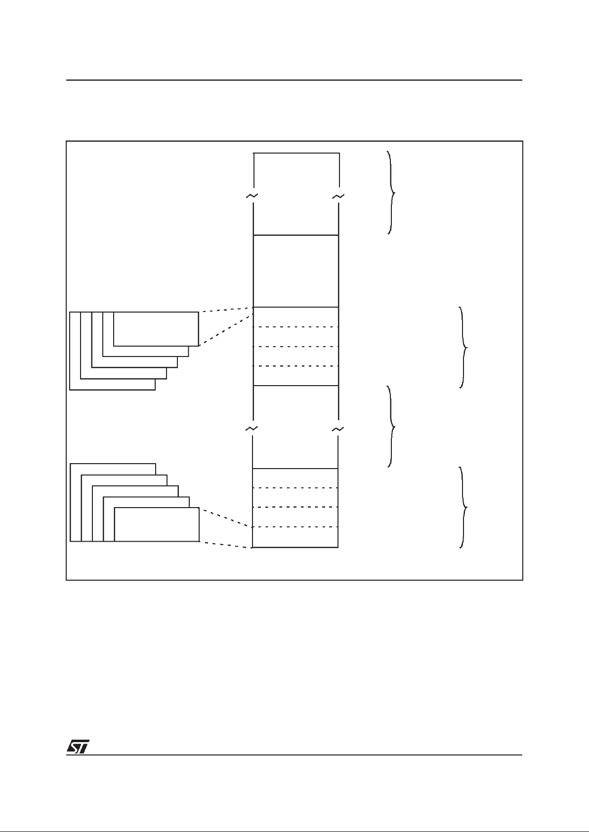
39/190
ST90158 - REGISTER AND MEMORY MAP
3.3 MEMORY MAP
Figure 18. Memory Map
010000h
00FFFFh
00C000h
00BFFFh
008000h
007FFFh
004000h
000000h
003FFFh
PAGE 0 - 16 Kbytes
PAGE 1 - 16 Kbytes
PAGE 2 - 16 Kbytes
PAGE 3 - 16 Kbytes
200000h
22FFFFh
20C000h
20BFFFh
208000h
207FFFh
204000h
203FFFh
PAGE 80 - 16 Kbytes
PAGE 81- 16 Kbytes
PAGE 82- 16 Kbytes
PAGE 83- 16 Kbytes
External
Memory
Reserved
External
Memory
SEGMENTS 21h and 22h
128 Kbytes
(external ROM on
20FFFFh
230000h
3FFFFFh
Lower Memory
(usually ROM/EPROM mapped
Upper Memory
(usually RAM mapped
210000h
Note: The total amount of directly addressable external memory is 64 Kbytes.
in Segment 1)
in Segment 23h)
1FFFFFh
000000h
003FFFh
ROM
16 Kbytes
Internal
24 Kbytes
32 Kbytes
48 Kbytes
64 Kbytes
00FFFFh
007FFFh
00BFFFh
00FFFFh
RAM
512 bytes
Internal
768 bytes
1 Kbytes
1.5 Kbytes
2 Kbytes
20F800h
20FA00h
20FC00h
20FD00h
20FE00h
20FFFFh
64 Kbytes
SEGMENT 0
64 Kbytes
SEGMENT20h
Internal ROM/EPROM
ROMless devices)
9

40/190
ST90158 - REGISTER AND MEMORY MAP
3.4 ST90158/135 REGISTER MAP
The following pages contain a list of ST90158/135
registers, grouped by peripheral or function.
Be very careful to correctly program both:
– The set of registers dedicated to a particular
function or peripheral.
– Registers common to other functions.
– In particular, double-check that any registers
with “undefined” resetvalues have been correct-
ly initialised.
Warning: Notethat in the EIVR and each IVR reg-
ister, all bits are significant. Takecare when defining base vector addresses that entriesin theInterrupt Vector table do not overlap.
Table 6. Common Registers
Function or Peripheral Common Registers
SCI, MFT CICR + NICR + DMA REGISTERS + I/O PORT REGISTERS
ADC CICR + NICR + I/O PORT REGISTERS
SPI, WDT, STIM
CICR + NICR + EXTERNAL INTERRUPT REGISTERS +
I/O PORT REGISTERS
I/O PORTS I/O PORT REGISTERS + MODER
EXTERNAL INTERRUPT INTERRUPT REGISTERS + I/O PORT REGISTERS
RCCU INTERRUPT REGISTERS + MODER
9

41/190
ST90158 - REGISTER AND MEMORY MAP
Table 7. Group F Pages
Resources available on the ST90158/ST90135 devices:
(*) ST90158/ST90E158 only. Not present on ST90135.
Register Page
0 2 3 8 9 10111213212425 43 5563
R255 Res.
Res.
PORT
7
MFT1
Res.
MFT0
(*)
Res.
MFT3
Res.
Res.
SCI0
SCI1
(*)
PORT
9
Res.
A/D
R254
SPI
R253
R252 WCR
R251
WDT
PORT
6
PORT
8
R250
PORT
2
R249
MMU
R248 MFT
R247
EXT
INT
Res. Res.
MFT1 MFT3
Res.
Res.
R246
PORT1PORT
5
EXT
MI
RCCU
R245
Res.R244
MMU
R243 Res. Res.
MFT0
(*)
STIM Res.
R242
PORT0PORT
4
RCCU
R241
Res.
Res.
R240 RCCU
9

42/190
ST90158 - REGISTER AND MEMORY MAP
Table 8. Detailed Register Map
Page
(Decimal)
Block
Reg.
No.
Register
Name
Description
Reset
Value
Hex.
N/A
Core
R230 CICR Central Interrupt Control Register 87
R231 FLAGR Flag Register 00
R232 RP0 Pointer 0 Register xx
R233 RP1 Pointer 1 Register xx
R234 PPR Page Pointer Register xx
R235 MODER Mode Register E0
R236 USPHR User Stack Pointer High Register xx
R237 USPLR User Stack Pointer Low Register xx
R238 SSPHR System Stack Pointer High Reg. xx
R239 SSPLR System Stack Pointer Low Reg. xx
I/O
Port
5:4,2:0
R224 P0DR Port 0 Data Register FF
R225 P1DR Port 1 Data Register FF
R226 P2DR Port 2 Data Register FF
R228 P4DR Port 4 Data Register FF
R229 P5DR Port 5 Data Register FF
0
INT
R242 EITR External Interrupt Trigger Register 00
R243 EIPR External Interrupt Pending Reg. 00
R244 EIMR External Interrupt Mask-bit Reg. 00
R245 EIPLR External Interrupt Priority Level Reg. FF
R246 EIVR External Interrupt Vector Register x6
R247 NICR Nested Interrupt Control 00
WDT
R248 WDTHR Watchdog Timer High Register FF
R249 WDTLR Watchdog Timer Low Register FF
R250 WDTPR Watchdog Timer Prescaler Reg. FF
R251 WDTCR Watchdog Timer Control Register 12
R252 WCR Wait Control Register 7F
SPI
R253 SPIDR SPI Data Register xx
R254 SPICR SPI Control Register 00
2
I/O
Port
0
R240 P0C0 Port 0 Configuration Register 0 00
R241 P0C1 Port 0 Configuration Register 1 00
R242 P0C2 Port 0 Configuration Register 2 00
I/O
Port
1
R244 P1C0 Port 1 Configuration Register 0 00
R245 P1C1 Port 1 Configuration Register 1 00
R246 P1C2 Port 1 Configuration Register 2 00
I/O
Port
2
R248 P2C0 Port 2 Configuration Register 0 FF
R249 P2C1 Port 2 Configuration Register 1 00
R250 P2C2 Port 2 Configuration Register 2 00
9

43/190
ST90158 - REGISTER AND MEMORY MAP
3
I/O
Port
4
R240 P4C0 Port 4 Configuration Register 0 FF
R241 P4C1 Port 4 Configuration Register 1 00
R242 P4C2 Port 4 Configuration Register 2 00
I/O
Port
5
R244 P5C0 Port 5 Configuration Register 0 FF
R245 P5C1 Port 5 Configuration Register 1 00
R246 P5C2 Port 5 Configuration Register 2 00
I/O
Port
6
R248 P6C0 Port 6 Configuration Register 0 FF
R249 P6C1 Port 6 Configuration Register 1 00
R250 P6C2 Port 6 Configuration Register 2 00
R251 P6DR Port 6 Data Register FF
I/O
Port
7
R252 P7C0 Port 7 Configuration Register 0 00/FF
R253 P7C1 Port 7 Configuration Register 1 00/00
R254 P7C2 Port 7 Configuration Register 2 00/00
R255 P7DR Port 7 Data Register FF
Page
(Decimal)
Block
Reg.
No.
Register
Name
Description
Reset
Value
Hex.
9

44/190
ST90158 - REGISTER AND MEMORY MAP
8
MFT1
R240 REG0HR1 Capture Load Register 0 High xx
R241 REG0LR1 Capture Load Register 0 Low xx
R242 REG1HR1 Capture Load Register 1 High xx
R243 REG1LR1 Capture Load Register 1 Low xx
R244 CMP0HR1 Compare 0 Register High 00
R245 CMP0LR1 Compare 0 Register Low 00
R246 CMP1HR1 Compare 1 Register High 00
R247 CMP1LR1 Compare 1 Register Low 00
R248 TCR1 Timer Control Register 0x
R249 TMR1 Timer Mode Register 00
R250 ICR1 External Input Control Register 0x
R251 PRSR1 Prescaler Register 00
R252 OACR1 Output A Control Register xx
R253 OBCR1 Output B Control Register xx
R254 FLAGR1 Flags Register 00
R255 IDMR1 Interrupt/DMA Mask Register 00
9
R244 DCPR0 DMA Counter Pointer Register xx
R245 DAPR0 DMA Address Pointer Register xx
R246 IVR0 Interrupt VectorRegister xx
R247 IDCR0 Interrupt/DMA Control Register C7
MFT0,1 R248 IOCR I/O Connection Register FC
MFT0
(*)
R240 DCPR1 DMA Counter Pointer Register xx
R241 DAPR1 DMA Address Pointer Register xx
R242 IVR1 Interrupt VectorRegister xx
R243 IDCR1 Interrupt/DMA Control Register C7
10
R240 REG0HR0 Capture Load Register 0 High xx
R241 REG0LR0 Capture Load Register 0 Low xx
R242 REG1HR0 Capture Load Register 1 High xx
R243 REG1LR0 Capture Load Register 1 Low xx
R244 CMP0HR0 Compare 0Register High 00
R245 CMP0LR0 Compare 0 Register Low 00
R246 CMP1HR0 Compare 1Register High 00
R247 CMP1LR0 Compare 1 Register Low 00
R248 TCR0 Timer Control Register 0x
R249 TMR0 Timer Mode Register 00
R250 ICR0 External Input Control Register 0x
R251 PRSR0 Prescaler Register 00
R252 OACR0 Output A Control Register xx
R253 OBCR0 Output B Control Register xx
R254 FLAGR0 Flags Register 00
R255 IDMR0 Interrupt/DMA Mask Register 00
Page
(Decimal)
Block
Reg.
No.
Register
Name
Description
Reset
Value
Hex.
9
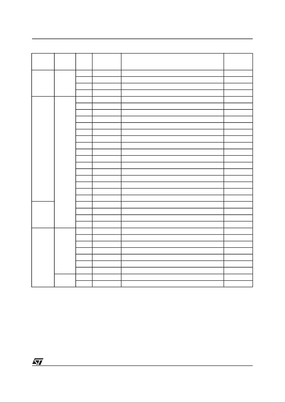
45/190
ST90158 - REGISTER AND MEMORY MAP
11 STIM
R240 STH Counter High Byte Register FF
R241 STL Counter Low Byte Register FF
R242 STP Standard Timer Prescaler Register FF
R243 STC Standard Timer Control Register 14
12
MFT3
R240 REG0HR1 Capture Load Register 0 High xx
R241 REG0LR1 Capture Load Register 0 Low xx
R242 REG1HR1 Capture Load Register 1 High xx
R243 REG1LR1 Capture Load Register 1 Low xx
R244 CMP0HR1 Compare 0Register High 00
R245 CMP0LR1 Compare 0 Register Low 00
R246 CMP1HR1 Compare 1Register High 00
R247 CMP1LR1 Compare 1 Register Low 00
R248 TCR1 Timer Control Register 0x
R249 TMR1 Timer Mode Register 00
R250 ICR1 External Input Control Register 0x
R251 PRSR1 Prescaler Register 00
R252 OACR1 Output A Control Register xx
R253 OBCR1 Output B Control Register xx
R254 FLAGR1 Flags Register 00
R255 IDMR1 Interrupt/DMA Mask Register 00
13
R244 DCPR0 DMA Counter Pointer Register xx
R245 DAPR0 DMA Address Pointer Register xx
R246 IVR0 Interrupt VectorRegister xx
R247 IDCR0 Interrupt/DMA Control Register C7
21
MMU
R240 DPR0 Data Page Register 0 xx
R241 DPR1 Data Page Register 1 xx
R242 DPR2 Data Page Register 2 xx
R243 DPR3 Data Page Register 3 xx
R244 CSR Code Segment Register 00
R248 ISR Interrupt Segment Register xx
R249 DMASR DMA Segment Register xx
EXTMI
R245 EMR1 External Memory Register 1 80
R246 EMR2 External Memory Register 2 0F
Page
(Decimal)
Block
Reg.
No.
Register
Name
Description
Reset
Value
Hex.
9

46/190
ST90158 - REGISTER AND MEMORY MAP
24 SCI0
R240 RDCPR0 Receiver DMA Transaction Counter Pointer xx
R241 RDAPR0 Receiver DMA Source Address Pointer xx
R242 TDCPR0 Transmitter DMA Transaction Counter Pointer xx
R243 TDAPR0 Transmitter DMA Destination Address Pointer xx
R244 IVR0 Interrupt VectorRegister xx
R245 ACR0 Address/Data Compare Register xx
R246 IMR0 Interrupt Mask Register x0
R247 ISR0 Interrupt Status Register xx
R248 RXBR0 Receive Buffer Register xx
R248 TXBR0 Transmitter Buffer Register xx
R249 IDPR0 Interrupt/DMA Priority Register xx
R250 CHCR0 Character Configuration Register xx
R251 CCR0 Clock Configuration Register 00
R252 BRGHR0 Baud Rate Generator High Reg. xx
R253 BRGLR0 Baud Rate Generator Low Register xx
R254 SICR0 Synchronous Input Control 03
R255 SOCR0 Synchronous Output Control 01
25
SCI1
(*)
R240 RDCPR1 Receiver DMA Transaction Counter Pointer xx
R241 RDAPR1 Receiver DMA Source Address Pointer xx
R242 TDCPR1 Transmitter DMA Transaction Counter Pointer xx
R243 TDAPR1 Transmitter DMA Destination Address Pointer xx
R244 IVR1 Interrupt VectorRegister xx
R245 ACR1 Address/Data Compare Register xx
R246 IMR1 Interrupt Mask Register x0
R247 ISR1 Interrupt Status Register xx
R248 RXBR1 Receive Buffer Register xx
R248 TXBR1 Transmitter Buffer Register xx
R249 IDPR1 Interrupt/DMA Priority Register xx
R250 CHCR1 Character Configuration Register xx
R251 CCR1 Clock Configuration Register 00
R252 BRGHR1 Baud Rate Generator High Reg. xx
R253 BRGLR1 Baud Rate Generator Low Register xx
R254 SICR1 Synchronous Input Control 03
R255 SOCR1 Synchronous Output Control 01
43
I/O
Port
8
R248 P8C0 Port 8 Configuration Register 0 00/03
R249 P8C1 Port 8 Configuration Register 1 00/00
R250 P8C2 Port 8 Configuration Register 2 00/00
R251 P8DR Port 8 Data Register FF
I/O
Port
9
R252 P9C0 Port 9 Configuration Register 0 00/00
R253 P9C1 Port 9 Configuration Register 1 00/00
R254 P9C2 Port 9 Configuration Register 2 00/00
R255 P9DR Port 9 Data Register FF
Page
(Decimal)
Block
Reg.
No.
Register
Name
Description
Reset
Value
Hex.
9

47/190
ST90158 - REGISTER AND MEMORY MAP
(*) Not present on ST90135.
Note: xx denotes a byte with an undefined value, however some of the bits may have defined values. Refer to register
description for details.
55 RCCU
R240 CLKCTL Clock Control Register 00
R242 CLK_FLAG Clock Flag Register 48, 28 or 08
R246 PLLCONF PLL Configuration Register xx
63 AD0
R240 D0R0 Channel 0 Data Register xx
R241 D1R0 Channel 1 Data Register xx
R242 D2R0 Channel 2 Data Register xx
R243 D3R0 Channel 3 Data Register xx
R244 D4R0 Channel 4 Data Register xx
R245 D5R0 Channel 5 Data Register xx
R246 D6R0 Channel 6 Data Register xx
R247 D7R0 Channel 7 Data Register xx
R248 LT6R0 Channel 6 Lower Threshold Reg. xx
R249 LT7R0 Channel 7 Lower Threshold Reg. xx
R250 UT6R0 Channel 6 Upper Threshold Reg. xx
R251 UT7R0 Channel 7 Upper Threshold Reg. xx
R252 CRR0 Compare Result Register 0F
R253 CLR0 Control Logic Register 00
R254 ICR0 Interrupt Control Register 0F
R255 IVR0 Interrupt VectorRegister x2
Page
(Decimal)
Block
Reg.
No.
Register
Name
Description
Reset
Value
Hex.
9

48/190
ST90158 - INTERRUPTS
4 INTERRUPTS
4.1 INTRODUCTION
The ST9 responds to peripheral and external
events through its interrupt channels. Current program execution can be suspended to allow the
ST9 to execute a specific response routine when
such an event occurs, providing that interrupts
have been enabled, and according to a priority
mechanism. If an event generates a valid interrupt
request, the current program status is saved and
control passes to the appropriate Interrupt Service
Routine.
The ST9 CPU can receive requests from the following sources:
– On-chip peripherals
– External pins
– Top-Level Pseudo-non-maskable interrupt
According to the on-chip peripheral features, an
event occurrence can generate an Interrupt request which depends on the selected mode.
Up to eight external interrupt channels, with programmable inputtrigger edge, areavailable. In addition, a dedicated interrupt channel, set to the
Top-level priority, can be devoted either to the external NMI pin (where available) to provide a NonMaskable Interrupt,or to the Timer/Watchdog. Interrupt service routines are addressed through a
vector table mapped in Memory.
Figure 19. Interrupt Response
n
4.2 INTERRUPT VECTORING
The ST9 implements an interrupt vectoring structure which allows the on-chip peripheral to identify
the location of the first instruction of the Interrupt
Service Routine automatically.
When an interrupt request is acknowledged, the
peripheral interrupt module provides, through its
Interrupt Vector Register (IVR), a vector to point
into the vector table of locations containing the
start addresses of the Interrupt Service Routines
(defined by the programmer).
Each peripheral has a specific IVR mapped within
its Register File pages.
The InterruptVector table, containing the addresses of the Interrupt Service Routines, is located in
the first 256 locations of Memory pointed to by the
ISR register, thus allowing 8-bit vector addressing.
For a description of the ISR register refer to the
chapter describing the MMU.
The user Power on Reset vector is stored in the
first two physical bytes in memory, 000000h and
000001h.
The Top Level Interrupt vector is located at addresses 0004h and 0005h in the segment pointed
to by the Interrupt Segment Register(ISR).
With one Interrupt Vector register, it is possible to
address several interrupt service routines; in fact,
peripherals can share the same interrupt vector
register among several interrupt channels. The
most significant bits of the vector are user programmable todefine thebase vector address within the vector table, the least significant bits are
controlled by the interrupt module, in hardware, to
select the appropriate vector.
Note: The first 256 locations of the memory segment pointedto by ISR can contain program code.
4.2.1 Divide by Zero trap
The Divide by Zero trap vector is located at addresses 0002h and 0003h of each code segment;
it should be noted that for each code segment a
Divide by Zero service routineis required.
Warning.Although the Divide by Zero Trap oper-
ates as an interrupt, the FLAG Register is not
pushed onto the system Stack automatically. As a
result it must be regarded as a subroutine, and the
service routine must end with the RET instruction
(not IRET ).
NORMAL
PROGRAM
FLOW
INTERRUPT
SERVICE
ROUTINE
IRET
INSTRUCTION
INTERRUPT
VR001833
CLEAR
PENDING BIT
9

49/190
ST90158 - INTERRUPTS
4.2.2 Segment Paging During Interrupt
Routines
The ENCSR bit in the EMR2 register can be used
to select between original ST9 backward compatibility mode and ST9+ interrupt management
mode.
ST9 backwardcompatibility mode(ENCSR =0)
If ENCSR is reset, the CPU works in original ST9
compatibility mode. For the duration of the interrupt service routine, ISR is used instead of CSR,
and the interruptstack frame is identical to that of
the original ST9: only the PC and Flags are
pushed.
This avoids saving the CSR on the stack in the
event of an interrupt, thus ensuring a faster interrupt response time.
It is not possible for an interrupt service routine to
perform inter-segment calls or jumps: these instructions would update the CSR, which, in this
case, is not used (ISR is used instead). The code
segment size for all interrupt service routines is
thus limited to 64K bytes.
ST9+ mode (ENCSR = 1)
If ENCSR is set, ISR is only used to point to the interrupt vector table and toinitialize the CSR at the
beginning of the interrupt service routine: the old
CSR ispushed onto the stack togetherwiththe PC
and flags, and CSR is then loaded with the contents of ISR.
In this case, iret will alsorestore CSR from the
stack. This approach allows interrupt service routines to access the entire 4 Mbytes of address
space. Thedrawback isthat the interruptresponse
time is slightly increased, because of the need to
also save CSR on the stack.
Full compatibilitywith the original ST9 is lost in this
case, because the interrupt stack frame is different.
4.3 INTERRUPT PRIORITY LEVELS
The ST9 supports a fully programmable interrupt
priority structure. Nine priority levels are available
to define the channel priorityrelationships:
– The on-chip peripheral channels and theeight
external interrupt sources can be programmed
within eight priority levels. Each channel has a 3-
bit field, PRL (Priority Level), that defines its pri-
ority level in the range from 0 (highest priority) to
7 (lowest priority).
– The 9th level (Top Level Priority) is reserved for
the Timer/Watchdog or the External Pseudo
Non-Maskable Interrupt. An Interrupt service
routine at this level cannot be interrupted in any
arbitration mode.Its mask can be bothmaskable
(TLI) or non-maskable (TLNM).
4.4 PRIORITY LEVEL ARBITRATION
The 3 bits of CPL (Current Priority Level) in the
Central Interrupt Control Register contain the priority of the currently running program (CPU priority). CPL isset to 7 (lowest priority) upon reset and
can be modified during program execution either
by software or automatically by hardware according to the selected Arbitration Mode.
During every instruction, an arbitration phase
takes place,during which, for every channel capable ofgenerating an Interrupt, each priority level is
compared to all the other requests (interrupts or
DMA).
If the highest priority request is an interrupt, its
PRL value mustbe strictly lower (that is, higherpriority) thanthe CPL value stored in theCICR register (R230) in order to be acknowledged. The Top
Level Interrupt overrides every other priority.
4.4.1 Priority level 7 (Lowest)
Interrupt requests at PRL level 7 cannot be acknowledged, as this PRL value (the lowest possible priority) cannot be strictly lower than the CPL
value. This can be of use in a fully polled interrupt
environment.
4.4.2 Maximum depth of nesting
No more than 8 routinescan be nested. If an interrupt routine at level N is being serviced, no other
Interrupts located at level N can interrupt it. This
guarantees amaximum numberof 8 nested levels
including the Top Level Interrupt request.
4.4.3 Simultaneous Interrupts
If twoor more requests occurat the same time and
at the same priority level, an on-chip daisy chain,
specific to every ST9 version, selects the channel
ENCSR Bit 0 1
Mode ST9 Compatible ST9+
Pushed/Popped
Registers
PC, FLAGR
PC, FLAGR,
CSR
Max. Code Size
for interrupt
service routine
64KB
Within 1segment
No limit
Across segments
9

50/190
ST90158 - INTERRUPTS
with thehighest position in the chain, as shown in
Figure 9
Table 9. Daisy Chain Priority
4.4.4 Dynamic Priority Level Modification
The main program androutines can be specifically
prioritized. Since the CPL is representedby 3 bits
in a read/write register, it is possible to modify dynamically the current priority valueduring program
execution. This means that a critical section can
have a higher priority with respect to other interrupt requests. Furthermore it is possible to prioritize even the Main Program execution by modifying the CPL during its execution. See Figure 20
Figure 20. Example of Dynamic priority
level modification in Nested Mode
4.5 ARBITRATION MODES
The ST9 provides two interrupt arbitration modes:
Concurrent mode and Nested mode. Concurrent
mode is the standard interrupt arbitration mode.
Nested mode improves the effective interrupt response time when service routine nesting is required, depending on the request prioritylevels.
The IAM control bit in the CICR Register selects
Concurrent Arbitration mode or Nested Arbitration
Mode.
4.5.1 Concurrent Mode
This mode is selected when the IAM bit is cleared
(reset condition). Thearbitration phase, performed
during every instruction, selects the request with
the highest priority level. The CPL value is not
modified in this mode.
Start of Interrupt Routine
The interrupt cycle performs the following steps:
– All maskable interrupt requests are disabled by
clearing CICR.IEN.
– The PC low byte is pushedonto system stack.
– The PC high byte is pushed onto systemstack.
– If ENCSR is set, CSR is pushedonto system
stack.
– The Flag register is pushed onto system stack.
– The PC is loaded with the 16-bitvector stored in
the Vector Table, pointed to bythe IVR.
– If ENCSR is set, CSR is loadedwith ISR con-
tents; otherwiseISR isused inplaceof CSR until
iret instruction.
End of Interrupt Routine
The Interrupt Service Routine must be ended with
the iret instruction. The iret instruction executes the following operations:
– The Flag register is popped fromsystem stack.
– If ENCSR is set, CSR is poppedfrom system
stack.
– The PC high byte is popped from system stack.
– The PC low byte is poppedfrom system stack.
– All unmasked Interrupts are enabled bysetting
the CICR.IEN bit.
– If ENCSR is reset, CSR is usedinstead of ISR.
Normal program execution thus resumesat the in-
terrupted instruction. All pending interrupts remain
pending until the next ei instruction (even if it is
executed during the interrupt service routine).
Note:In Concurrentmode, the source priority level
is only useful during thearbitration phase,where it
is compared with all other priority levels and with
the CPL. No trace is kept of its value during the
ISR. If other requests are issued during the interrupt service routine, once the global CICR.IEN is
re-enabled, they will be acknowledged regardless
of the interrupt service routine’s priority. This may
cause undesirable interrupt response sequences.
Highest Position
Lowest Position
INTA0
INTA1
INTB0
INTB1
INTC0
INTC1
INTD0
INTD1
TIMER0
SCI0
SCI1
A/D
TIMER3
TIMER1
INT0/WDT
INT1
INT2/SPI
INT3
INT4/STIM
INT5
INT6/RCCU
INT7
6
5
4
7
Priority Level
MAIN
CPL is set to 5
CPL=7
MAIN
INT 6
CPL=6
INT6
ei
CPL is set to 7
CPL6 > CPL5:
INT6 pending
INTERRUPT 6 HAS PRIORITY LEVEL 6
by MAIN program
9

51/190
ST90158 - INTERRUPTS
ARBITRATION MODES (Cont’d)
Examples
In the following two examples, three interrupt requests with different priority levels (2, 3 & 4) occur
simultaneously during the interrupt 5 service routine.
Example 1
In the firstexample, (simplest case, Figure21) the
ei instruction is not used within the interrupt service routines. This means that no new interrupt can
be serviced in the middle of the current one. The
interrupt routines will thus be serviced one after
another, in the order of their priority, until the main
program eventually resumes.
Figure 21. Simple Example of a Sequence of Interrupt Requests with:
- Concurrent mode selected and
- IEN unchanged by the interrupt routines
6
5
4
3
2
1
0
7
Priority Level of
MAIN
INT 5
INT 2
INT 3
INT 4
MAIN
INT 5
INT4
INT3
INT2
CPL is set to 7
CPL = 7
CPL = 7
CPL = 7
CPL = 7
CPL = 7
ei
INTERRUPT 2 HAS PRIORITY LEVEL 2
INTERRUPT 3 HAS PRIORITY LEVEL 3
INTERRUPT 4 HAS PRIORITY LEVEL 4
INTERRUPT 5 HAS PRIORITY LEVEL 5
Interrupt Request
9

52/190
ST90158 - INTERRUPTS
ARBITRATION MODES (Cont’d)
Example 2
In the second example, (more complex, Figure
22), each interrupt service routine sets Interrupt
Enable with the ei instruction at the beginning of
the routine. Placed here, it minimizes response
time forrequests with ahigher priority thanthe one
being serviced.
The level 2 interrupt routine (with the highest priority) will be acknowledged first, then, when the ei
instruction is executed, it will beinterrupted by the
level 3 interrupt routine, which itself will be interrupted by the level 4 interrupt routine. When the
level 4interrupt routineis completed,the level 3interrupt routineresumes andfinally the level2 interrupt routine.This results in the three interrupt serv-
ice routines being executed in the opposite order
of their priority.
It is therefore recommended to avoid inserting
the ei instruction in the interrupt service routine in Concurrent mode. Use the ei instruction only in nested mode.
WARNING: If, in Concurrent Mode, interrupts are
nested (by executing ei in an interrupt service
routine), make sure that either ENCSR is set or
CSR=ISR, otherwisetheiret of the innermostinterrupt will makethe CPU useCSR instead of ISR
before the outermost interrupt service routine is
terminated, thusmaking the outermost routine fail.
Figure 22. Complex Example of a Sequence of Interrupt Requests with:
- Concurrent mode selected
- IEN set to 1 during interrupt service routine execution
6
5
4
3
2
1
0
7
MAIN
INT 5
INT 2
INT 3
INT 4
INT 5
INT4
INT3
INT2
CPL is set to 7
CPL = 7
CPL = 7
CPL = 7
CPL = 7
CPL = 7
ei
INTERRUPT2 HAS PRIORITY LEVEL 2
INTERRUPT3 HAS PRIORITY LEVEL 3
INTERRUPT4 HAS PRIORITY LEVEL 4
INTERRUPT5 HAS PRIORITY LEVEL 5
INT 2
INT 3
CPL = 7
CPL = 7
INT 5
CPL = 7
MAIN
ei
ei
ei
Priority Level of
Interrupt Request
ei
9

53/190
ST90158 - INTERRUPTS
ARBITRATION MODES (Cont’d)
4.5.2 Nested Mode
The difference between Nested mode and Concurrent mode, lies in the modification of the Current Priority Level (CPL) during interrupt processing.
The arbitration phase is basically identical to Concurrent mode, however, once the request is acknowledged, the CPL is saved in theNested Interrupt Control Register (NICR) by setting the NICR
bit corresponding to the CPL value (i.e. if the CPL
is 3, the bit 3 will be set).
The CPL is then loaded with the priority of the request justacknowledged; the next arbitration cycle
is thus performed with reference to the priority of
the interrupt service routine currently being executed.
Start of Interrupt Routine
The interrupt cycle performs the followingsteps:
– All maskable interrupt requests are disabled by
clearing CICR.IEN.
– CPL is saved in the special NICR stack to hold
the priority level of the suspended routine.
– Priority level of the acknowledged routine is
stored in CPL, so that the nextrequest priority
will be compared with the one ofthe routine cur-
rently being serviced.
– The PC low byte is pushedonto system stack.
– The PC high byte is pushed onto systemstack.
– If ENCSR is set, CSR is pushedonto system
stack.
– The Flag register is pushed onto system stack.
– The PC is loaded with the 16-bitvector stored in
the Vector Table, pointed to bythe IVR.
– If ENCSR is set, CSR is loadedwith ISR con-
tents; otherwiseISR isused inplaceof CSR until
iret instruction.
Figure 23. Simple Example of a Sequence of Interrupt Requests with:
- Nested mode
- IEN unchanged by the interrupt routines
6
5
4
3
2
1
0
7
MAIN
INT 2
INT0
INT4
INT3
INT2
CPL is set to 7
CPL=2
CPL=7
ei
INTERRUPT2 HAS PRIORITY LEVEL 2
INTERRUPT3 HAS PRIORITY LEVEL 3
INTERRUPT4 HAS PRIORITY LEVEL 4
INTERRUPT5 HAS PRIORITY LEVEL 5
MAIN
INT 3
CPL=3
INT6
CPL=6
INT5
INT 0
CPL=0
INT6
INT2
INTERRUPT6 HAS PRIORITY LEVEL 6
INTERRUPT0 HAS PRIORITY LEVEL 0
CPL6 > CPL3:
INT6 pending
CPL2 < CPL4:
Serviced next
INT 2
CPL=2
INT 4
CPL=4
INT 5
CPL=5
Priority Level of
Interrupt Request
9

54/190
ST90158 - INTERRUPTS
ARBITRATION MODES (Cont’d)
End of Interrupt Routine
The iret Interrupt Return instruction executes
the following steps:
– The Flag registeris popped from system stack.
– If ENCSR is set, CSR is popped from system
stack.
– The PC high byte is popped from system stack.
– The PC low byte is popped from system stack.
– All unmasked Interrupts are enabled by setting
the CICR.IEN bit.
– The priority level of the interrupted routine is
popped from the special register (NICR) and
copied into CPL.
– If ENCSR is reset, CSR is usedinstead of ISR,
unless the program returns to anothernested
routine.
The suspended routine thus resumes at the interrupted instruction.
Figure 23 contains a simple example, showing that
if the ei instruction is not used in the interrupt
service routines, nested and concurrent modes
are equivalent.
Figure 24 contains a more complex example
showing how nested mode allows nested interrupt
processing (enabled inside the interrupt service
routinesi using the ei instruction) according to
their priority level.
Figure 24. Complex Example of a Sequence of Interrupt Requests with:
- Nested mode
- IEN set to 1 during the interrupt routine execution
INT 2
INT 3
CPL=3
INT 0
CPL=0
INT6
6
5
4
3
2
1
0
7
MAIN
INT5
INT 4
INT0
INT4
INT3
INT2
CPL is set to 7
CPL=5
CPL=4
CPL=2
CPL=7
ei
INTERRUPT 2 HAS PRIORITY LEVEL 2
INTERRUPT 3 HAS PRIORITY LEVEL 3
INTERRUPT 4 HAS PRIORITY LEVEL 4
INTERRUPT 5 HAS PRIORITY LEVEL 5
INT 2
INT 4
CPL=2
CPL=4
INT 5
CPL=5
MAIN
ei
ei
INT 2
CPL=2
INT 6
CPL=6
INT5
INT2
ei
INTERRUPT 6 HAS PRIORITY LEVEL 6
INTERRUPT 0 HAS PRIORITY LEVEL 0
CPL6 > CPL3:
INT6 pending
CPL2 < CPL4:
Serviced just after ei
Priority Level of
Interrupt Request
ei
9
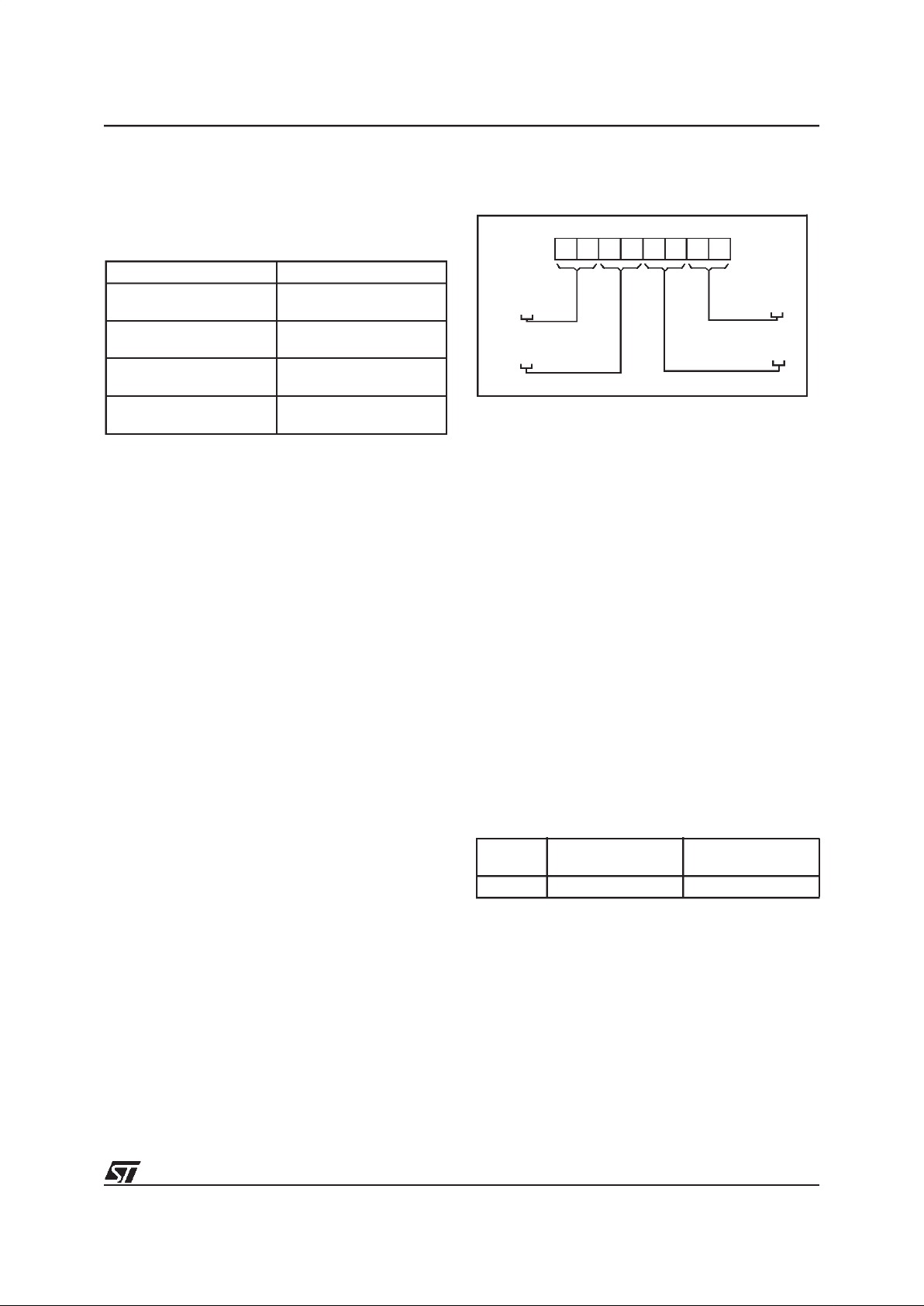
55/190
ST90158 - INTERRUPTS
4.6 EXTERNAL INTERRUPTS
The standard ST9 core contains 8 external interrupts sources grouped into four pairs.
Table 10. External Interrupt Channel Grouping
Each source has atrigger control bit TEA0,..TED1
(R242,EITR.0,..,7 Page 0) to select triggering on
the rising or falling edge of the external pin. If the
Trigger control bit is set to “1”, the corresponding
pending bit IPA0,..,IPD1 (R243,EIPR.0,..,7 Page
0) is set on the input pin rising edge, if it is cleared,
the pending bit is set on the falling edge of the input pin. Each source can be individually masked
through the corresponding control bit
IMA0,..,IMD1 (EIMR.7,..,0). See Figure 26.
The priority level of the external interrupt sources
can be programmed among the eight priority levels with the control register EIPLR (R245). The priority level of each pair is software defined using
the bits PRL2, PRL1. For each pair, the even
channel (A0,B0,C0,D0) of the group has the even
priority level and the odd channel (A1,B1,C1,D1)
has the odd (lower) priority level.
Figure 25. Priority Level Examples
n
Figure 25 shows an example of priority levels.
Figure 26 gives an overview of the External inter-
rupt control bits and vectors.
– The source of the interrupt channel A0 can be
selected between the external pin INT0 (when
IA0S = “1”, thereset value) or the On-chip Timer/
Watchdog peripheral (when IA0S = “0”).
– The source of the interrupt channel B0 can be
selected between the external pin INT2 (when
(SPEN,BMS)=(0,0)) or the on-chip SPI peripheral.
– The source of the interrupt channel C0 can be
selected between the external pin INT4 (when
INTS = “1”) or the on-chip Standard Timer.
– The source of the interrupt channel D0 can be
selected between the external pin INT6 (when
INT_SEL = “0”) or the on-chip RCCU.
Warning: When using channels shared by both
external interrupts and peripherals, special care
must be taken to configure their control registers
for both peripherals and interrupts.
Table 11. Multiplexed Interrupt Sources
External Interrupt Channel
INT7
INT6
INTD1
INTD0
INT5
INT4
INTC1
INTC0
INT3
INT2
INTB1
INTB0
INT1
INT0
INTA1
INTA0
Channel
Internal Interrupt
Source
External Interrupt
Source
INTA0 Timer/Watchdog INT0
1 001001
PL2DPL1D PL2CPL1C PL2B PL1B PL2APL1A
INT.D1:
INT.C1: 001=1
INT.D0:
SOURCE PRIORITY PRIORITYSOURCE
INT.A0: 010=2
INT.A1: 011=3
INT.B1: 101=5
INT.B0: 100=4INT.C0: 000=0
EIPLR
VR000151
0
100=4
101=5
9

56/190
ST90158 - INTERRUPTS
EXTERNAL INTERRUPTS (Cont’d)
Figure 26. External Interrupts Control Bits and
Vectors
n
n
INT A0
request
VECTOR
Priority level
Mask bit Pending bit
IMA0
IPA0
V7V6V5 V4 0
000
“0”
“1”
IA0S
Watchdog/Timer
End of count
INT 0 pin
INT A1
request
TEA1
INT 1 pin
INT B0
request
INT 2 pin
INT B1
request
TEB1
INT 3 pin
INT C0
request
INT 4 pin
INT C1
request
TEC1
INT 5 pin
INT D0
request
TED0
INT 6 pin
INT D1
request
TED1
INT 7 pin
VECTOR
Priority level
Mask bit Pending bit
IMA1
IPA1
V7V6 V5 V4 0
010
1
V7 V6 V5 V4 0
100
V7V6V5 V4 0
110
V7
V6
V5 V4 1
000
V7
V6
V5 V4
1010
V7 V6 V5 V4 1
100
V7
V6
V5 V4 1
110
VECTOR
Priority level
VECTOR
Priority level
VECTOR
Priority level
VECTOR
Priority level
VECTOR
Priority level
VECTOR
Priority level
Mask bit
IMB0
Pending bit IPB0
Pending bit IPB1
Pending bit IPC0
Pending bit IPC1
Pending bit IPD0
Pending bit IPD1
Mask bit
IMB1
Mask bit IMC0
Mask bit
IMC1
Mask bit IMD0
Mask bit IMD1
*
Shared channels, see warning
*
*
SPEN,BMS
SPI Interrupt
INTS
STD Timer
“1”
“0”
INT_SEL
RCCU
“0”
“1”
TEA0
TEC0
TEB0
*
*
“0,0”
PL2A PL1A
1
PL2C PL1C
0
PL2B PL1B
0
PL2A PL1A
1
PL2B PL1B
0
PL2C PL1C
0
PL2D PL1D
1
PL2D PL1D
9

57/190
ST90158 - INTERRUPTS
4.7 TOP LEVEL INTERRUPT
The Top Level Interrupt channel can be assigned
either to the external pin NMI or to the Timer/
Watchdog according to the status ofthe control bit
EIVR.TLIS (R246.2, Page 0). If this bit is high (the
reset condition)the source is the external pin NMI.
If it is low, the source is the Timer/ Watchdog End
Of Count. When the source is the NMI external
pin, the control bit EIVR.TLTEV (R246.3; Page 0)
selects betweenthe rising (if set)or falling (if reset)
edge generating the interrupt request. When the
selected event occurs, the CICR.TLIP bit (R230.6)
is set. Depending on the mask situation, a Top
Level Interrupt request may be generated. Two
kinds of masks are available, a Maskable mask
and a Non-Maskable mask. The first mask is the
CICR.TLI bit (R230.5): it can be set or cleared to
enable or disable respectively theTop Level Interrupt request. If itis enabled, the global Enable Interrupt bit, CICR.IEN (R230.4) must also be enabled in order to allow a Top Level Request.
The second mask NICR.TLNM (R247.7) is a setonly mask. Once set, it enables the Top Level Interrupt request independently of the value of
CICR.IEN and it cannot be cleared by the program. Only the processor RESET cycle can clear
this bit. This does not prevent theuser from ignoring some sources due to a change in TLIS.
The TopLevel Interrupt Service Routine cannot be
interrupted by any other interruptor DMA request,
in any arbitration mode, not even by a subsequent
Top Level Interrupt request.
Warning. The interrupt machine cycle of the Top
Level Interrupt does not clear the CICR.IEN bit,
and the corresponding iret does not set it. Furthermore the TLI never modifies the CPL bits and
the NICR register.
4.8 ON-CHIP PERIPHERAL INTERRUPTS
The general structure of the peripheral interrupt
unit is described here, however each on-chip peripheral has its own specific interrupt unitcontaining one or more interrupt channels, or DMA channels. Please refer to the specific peripheral chapter for the description of its interrupt features and
control registers.
The on-chip peripheral interrupt channels provide
the following control bits:
– Interrupt Pending bit (IP). Set by hardware
when the Trigger Event occurs.Can be set/
cleared by software to generate/cancel pending
interrupts andgive the status for Interruptpolling.
– Interrupt Mask bit (IM). If IM = “0”, no interrupt
request is generated. If IM =“1” an interrupt request is generated whenever IP = “1” and
CICR.IEN = “1”.
– Priority Level (PRL, 3 bits). These bits define
the current priority level, PRL=0: thehighest priority, PRL=7: the lowest priority (the interrupt
cannot be acknowledged)
– Interrupt Vector Register (IVR, up to 7 bits).
The IVR points to the vectortable which itself
contains the interrupt routine start address.
Figure 27. Top Level Interrupt Structure
n
n
WATCHDOG ENABLE
WDEN
WATCHDOG TIMER
END OF COUNT
NMI OR
TLTEV
MUX
TLIS
TLIP
TLNM
TLI
IEN
PENDING
MASK
TOP LEVEL
INTERRUPT
VA00294
CORE
RESET
REQUEST
9

58/190
ST90158 - INTERRUPTS
4.9 INTERRUPT RESPONSE TIME
The interrupt arbitration protocol functions completely asynchronously from instruction flow and
requires 5 clock cycles. One more CPUCLK cycle
is required when an interrupt is acknowledged.
Requests are sampled every 5 CPUCLK cycles.
If the interrupt request comes from an externalpin,
the trigger event must occur a minimum of one
INTCLK cycle before thesampling time.
When an arbitration results in an interrupt request
being generated, the interrupt logic checks if the
current instruction (which could be at any stage of
execution) can be safely aborted; if this is the
case, instruction execution is terminated immediately and the interrupt request is serviced; if not,
the CPU waits until the current instruction is terminated and then services the request. Instruction
execution can normally be aborted provided no
write operation has been performed.
For an interrupt deriving from an external interrupt
channel, the response time between a user event
and the start of the interrupt service routine can
range froma minimum of 26 clock cyclesto amaximum of 55 clock cycles (DIV instruction), 53 clock
cycles (DIVWS and MUL instructions) or 49 for
other instructions.
For a non-maskable Top Level interrupt, the response time between a user event and the start of
the interrupt service routine can range from a minimum of 22 clock cycles to amaximum of 51 clock
cycles (DIV instruction), 49 clock cycles (DIVWS
and MUL instructions) or45 for other instructions.
In orderto guaranteeedge detection, input signals
must be kept low/high for a minimum of one
INTCLK cycle.
An interrupt machine cycle requires a basic 18 internal clock cycles (CPUCLK), to which must be
added a further 2 clock cycles if thestack is in the
Register File. 2 more clock cycles must further be
added if the CSR is pushed (ENCSR =1).
The interrupt machine cycle duration forms part of
the two examples of interrupt responsetime previously quoted; it includes the time required to push
values on the stack, as well as interrupt vector
handling.
In Wait for Interrupt mode, a further cycle is required as wake-up delay.
9

59/190
ST90158 - INTERRUPTS
4.10 INTERRUPT REGISTERS
CENTRAL INTERRUPT CONTROL REGISTER
(CICR)
R230 - Read/Write
Register Group: System
Reset value: 1000 0111 (87h)
Bit 7 = GCEN:
Global Counter Enable.
This bit enables the 16-bit Multifunction Timer peripheral.
0: MFT disabled
1: MFT enabled
Bit 6 = TLIP:
Top Level Interrupt Pending
.
This bit is set by hardware when Top Level Interrupt (TLI) trigger event occurs. It is cleared by
hardware when a TLI is acknowledged. It can also
be set by software to implementa software TLI.
0: No TLI pending
1: TLI pending
Bit 5 = TLI:
Top Level Interrupt.
This bit is set and cleared bysoftware.
0: ATopLevel Interruptis generared when TLIP is
set, only if TLNM=1 in the NICR register (independently of the value of the IEN bit).
1: A Top Level Interrupt requestisgenerated when
IEN=1 and the TLIP bit are set.
Bit 4 = IEN:
Interrupt Enable
.
This bit is cleared by the interrupt machine cycle
(except for a TLI).
It isset by the iret instruction (except for a return
from TLI).
It is set by the EI instruction.
It is cleared by the DI instruction.
0: Maskable interrupts disabled
1: Maskable Interrupts enabled
Note: The IEN bit can also be changed by software using any instruction that operates on register CICR, however in this case, take care to avoid
spurious interrupts,since IEN cannot be clearedin
the middle of an interrupt arbitration. Only modify
the IEN bit when interrupts are disabled or when
no peripheral can generate interrupts. For example, if the state of IEN is not known in advance,
and its value must be restored from a previous
push of CICR on the stack, usethe sequence DI;
POP CICR to make sure that no interruptsare being arbitrated when CICR is modified.
Bit 3 =IAM:
Interrupt Arbitration Mode
.
This bit is set andcleared by software.
0: Concurrent Mode
1: Nested Mode
Bit 2:0 = CPL[2:0]:
Current Priority Level
.
These bits define the Current Priority Level.
CPL=0 is the highest priority. CPL=7 is the lowest
priority. Thesebits may be modified directly by the
interrupt hardware when Nested Interrupt Mode is
used.
EXTERNAL INTERRUPT TRIGGER REGISTER
(EITR)
R242 - Read/Write
Register Page: 0
Reset value: 0000 0000 (00h)
Bit 7 =TED1:
INTD1 Trigger Event
Bit 6 =TED0:
INTD0 Trigger Event
Bit 5 =TEC1:
INTC1 Trigger Event
Bit 4 =TEC0:
INTC0 Trigger Event
Bit 3 =TEB1:
INTB1 Trigger Event
Bit 2 =TEB0:
INTB0 Trigger Event
Bit 1 =TEA1:
INTA1 Trigger Event
Bit 0 =TEA0:
INTA0 Trigger Event
These bits are set and cleared by software.
0: Select falling edge asinterrupt trigger event
1: Select rising edge as interrupt trigger event
70
GCEN TLIP TLI IEN IAM CPL2 CPL1 CPL0
70
TED1 TED0 TEC1 TEC0 TEB1 TEB0 TEA1 TEA0
9

60/190
ST90158 - INTERRUPTS
INTERRUPT REGISTERS (Cont’d)
EXTERNAL INTERRUPT PENDING REGISTER
(EIPR)
R243 - Read/Write
Register Page: 0
Reset value: 0000 0000 (00h)
Bit 7 = IPD1:
INTD1 Interrupt Pending bit
Bit 6 = IPD0:
INTD0 Interrupt Pending bit
Bit 5 = IPC1:
INTC1 Interrupt Pending bit
Bit 4 = IPC0:
INTC0 Interrupt Pending bit
Bit 3 = IPB1:
INTB1 Interrupt Pending bit
Bit 2 = IPB0:
INTB0 Interrupt Pending bit
Bit 1 = IPA1:
INTA1 Interrupt Pending bit
Bit 0 = IPA0:
INTA0 Interrupt Pending bit
These bits are set byhardware on occurrence of a
trigger event (as specified in the EITR register)
and are cleared by hardware on interrupt acknowledge. They can also be set by software to implement a software interrupt.
0: No interrupt pending
1: Interrupt pending
EXTERNAL INTERRUPT MASK-BIT REGISTER
(EIMR)
R244 - Read/Write
Register Page: 0
Reset value: 0000 0000 (00h)
Bit 7 = IMD1:
INTD1 Interrupt Mask
Bit 6 = IMD0:
INTD0 Interrupt Mask
Bit 5 = IMC1:
INTC1 Interrupt Mask
Bit 4 = IMC0:
INTC0 Interrupt Mask
Bit 3 =IMB1:
INTB1 Interrupt Mask
Bit 2 =IMB0:
INTB0 Interrupt Mask
Bit 1 =IMA1:
INTA1 Interrupt Mask
Bit 0 =IMA0:
INTA0 Interrupt Mask
These bits are set and cleared by software.
0: Interrupt masked
1: Interrupt notmasked (aninterrupt isgenerated if
the IPxx and IEN bits = 1)
EXTERNAL INTERRUPT PRIORITY LEVEL
REGISTER (EIPLR)
R245 - Read/Write
Register Page: 0
Reset value: 1111 1111 (FFh)
Bit 7:6 = PL2D, PL1D:
INTD0, D1 Priority Level.
Bit 5:4 = PL2C, PL1C:
INTC0, C1 Priority Level.
Bit 3:2 = PL2B, PL1B:
INTB0, B1 Priority Level.
Bit 1:0 = PL2A, PL1A:
INTA0, A1 Priority Level.
These bits are set and cleared by software.
The priority is a three-bit value. TheLSB is fixedby
hardware at0for Channels A0,B0, C0 andD0 and
at 1 for Channels A1, B1, C1 and D1.
70
IPD1 IPD0 IPC1 IPC0 IPB1 IPB0 IPA1 IPA0
70
IMD1 IMD0 IMC1 IMC0 IMB1 IMB0 IMA1 IMA0
70
PL2D PL1D PL2C PL1C PL2B PL1B PL2A PL1A
PL2x PL1x
Hardware
bit
Priority
00
0
1
0 (Highest)
1
01
0
1
2
3
10
0
1
4
5
11
0
1
6
7 (Lowest)
9

61/190
ST90158 - INTERRUPTS
INTERRUPT REGISTERS (Cont’d)
EXTERNAL INTERRUPT VECTOR REGISTER
(EIVR)
R246 - Read/Write
Register Page: 0
Reset value: xxxx 0110b (x6h)
Bit 7:4 = V[7:4]:
Most significant nibbleof External
Interrupt Vector
.
These bits are not initialized by reset. For a representation of how the full vector is generated from
V[7:4] and the selected external interrupt channel,
refer to Figure 26.
Bit 3 = TLTEV:
Top Level Trigger Event bit.
This bit is set and cleared bysoftware.
0: Select falling edge as NMI trigger event
1: Select rising edge as NMItrigger event
Bit 2 = TLIS:
Top Level Input Selection
.
This bit is set and cleared bysoftware.
0: Watchdog End of Count is TL interrupt source
1: NMI is TL interrupt source
Bit 1 = IA0S:
Interrupt Channel A0 Selection.
This bit is set and cleared bysoftware.
0: Watchdog End of Count is INTA0 source
1: External Interrupt pin isINTA0 source
Bit 0 = EWEN:
External Wait Enable.
This bit is set and cleared bysoftware.
0: WAITN pin disabled
1: WAITN pin enabled (to stretch the external
memory access cycle).
Note: For more details on Wait mode refer to the
section describing the WAITN pin in the External
Memory Chapter.
NESTED INTERRUPT CONTROL (NICR)
R247 - Read/Write
Register Page: 0
Reset value: 0000 0000 (00h)
Bit 7 =TLNM:
Top Level Not Maskable
.
This bit is set by software and cleared only by a
hardware reset.
0: Top Level Interrupt Maskable. A top level re-
quest is generated if the IEN, TLI and TLIP bits
=1
1: Top Level Interrupt Not Maskable. A top level
request is generated if the TLIPbit =1
Bit 6:0 = HL[6:0]:
Hold Level
x
These bits are set by hardware when, in Nested
Mode, an interrupt service routine at level x is interrupted from a request with higher priority (other
than the Top Level interrupt request). They are
cleared by hardware at the iret execution when
the routine at level xis recovered.
70
V7 V6 V5 V4 TLTEV TLIS IAOS EWEN
70
TLNM HL6 HL5 HL4 HL3 HL2 HL1 HL0
9

62/190
ST90158 - INTERRUPTS
INTERRUPT REGISTERS (Cont’d)
EXTERNAL MEMORY REGISTER 2 (EMR2)
R246 - Read/Write
Register Page: 21
Reset value: 0000 1111 (0Fh)
Bit 7, 5:0 = Reserved, keep in reset state. Refer to
the external Memory Interface Chapter.
Bit 6 = ENCSR:
Enable Code Segment Register.
This bit is set and cleared by software. It affects
the ST9 CPU behaviour whenever an interrupt request is issued.
0: The CPU works in original ST9 compatibility
mode. For the duration of the interruptservice
routine, ISR is used instead of CSR, and the interrupt stack frame isidentical to that of the original ST9: only the PC and Flags are pushed.
This avoids saving the CSR on the stackin the
event of an interrupt, thus ensuring afaster in-
terrupt response time.The drawback isthat it is
not possible for an interrupt service routine to
perform inter-segment calls or jumps: these instructions would update the CSR, which, in this
case, is not used (ISR is used instead). The
code segment size for all interruptservice routines is thus limited to 64K bytes.
1: ISR is only used to pointto theinterrupt vector
table and to initialize the CSR atthe beginning
of the interrupt service routine: the old CSR is
pushed ontothe stack togetherwith the PCand
flags, and CSRis thenloaded with the contents
of ISR. In this case, iret will also restore CSR
from the stack. This approach allows interrupt
service routinesto accesstheentire 4Mbytes of
address space; the drawback is thatthe interrupt response time is slightly increased, because of the need to also save CSR on the
stack. Full compatibility with the originalST9 is
lost in this case, because the interrupt stack
frame is different; this difference, however,
should not affect the vast majority of programs.
70
0 ENCSR 0 0 1 1 1 1
9

63/190
ST90158 - ON-CHIP DIRECT MEMORY ACCESS (DMA)
5 ON-CHIP DIRECT MEMORY ACCESS (DMA)
5.1 INTRODUCTION
The ST9 includes on-chip Direct Memory Access
(DMA) in order to provide high-speed data transfer
between peripherals andmemory or Register File.
Multi-channel DMA is fully supported by peripherals having their own controller and DMA channel(s). Each DMA channel transfers data to or
from contiguouslocations inthe RegisterFile, or in
Memory. The maximum number of bytes that can
be transferred per transaction by each DMA channel is 222 with the Register File, or 65536 with
Memory.
The DMA controller in the Peripheral uses an indirect addressing mechanism to DMA Pointers and
Counter Registers storedin the Register File. This
is the reason why the maximum number of transactions for the Register Fileis 222, since two Registers are allocated for the Pointer and Counter.
Register pairs are used for memory pointers and
counters in order to offer the full 65536 byte and
count capability.
5.2 DMA PRIORITY LEVELS
The 8 priority levels used for interrupts are also
used to prioritize the DMA requests, which are arbitrated in the same arbitration phase as interrupt
requests. If the event occurrence requires a DMA
transaction, this will take place at the end of the
current instruction execution. When an interrupt
and a DMA request occur simultaneously, on the
same priority level, the DMA request is serviced
before the interrupt.
An interrupt priority request mustbe strictly higher
than the CPL value in order to be acknowledged,
whereas, for aDMA transaction request, it must be
equal to or higher than the CPL value in order to
be executed. Thus only DMA transaction requests
can be acknowledged when the CPL=0.
DMA requests do not modify the CPL value, since
the DMA transaction is notinterruptable.
Figure 28. DMA Data Transfer
PERIPHERAL
VR001834
DATA
ADDRESS
COUNTER
TRANSFERRED
REGISTER FILE
OR
MEMORY
REGISTER FILE
REGISTER FILE
START ADDRESS
COUNTER VALUE
0
DF
DATA
GROUP F
PERIPHERAL
PAGED
REGISTERS
9

64/190
ST90158 - ON-CHIP DIRECT MEMORY ACCESS (DMA)
5.3 DMA TRANSACTIONS
The purpose of an on-chip DMA channel is to
transfer a block of data between a peripheral and
the Register File, or Memory. Each DMA transfer
consists of three operations:
– A load from/to the peripheral data register to/
from a location of Register File (or Memory) addressed through the DMA Address Register (or
Register pair)
– A post-increment of the DMA Address Register
(or Register pair)
– Apost-decrement of the DMA transaction coun-
ter, which contains the number of transactions
that have still to be performed.
If the DMA transaction is carried out between the
peripheral and the Register File (Figure 29), one
register is required to hold the DMA Address, and
one to hold the DMA transaction counter. These
two registers must be located in the RegisterFile:
the DMA Address Register in the even address
register, and the DMA Transaction Counter in the
next register (odd address). They arepointed to by
the DMA Transaction Counter Pointer Register
(DCPR), located in the peripheral’s paged registers. In order to select a DMA transaction with the
Register File, the control bit DCPR.RM (bit 0 of
DCPR) must be set.
If the transaction is made between the peripheral
and Memory, a register pair (16 bits) is required
for the DMA Address and the DMA Transaction
Counter (Figure 30). Thus, two register pairs must
be located in the Register File.
The DMA Transaction Counter is pointed to bythe
DMA Transaction Counter Pointer Register
(DCPR), the DMA Address is pointed to by the
DMA Address Pointer Register (DAPR),both
DCPR and DAPR are located in the paged registers of the peripheral.
Figure 29. DMA Between Register File and Peripheral
IDCR
IVR
DAPR
DCPR
DATA
PAGED
REGISTERS
REGISTERS
SYSTEM
DMA
COUNTER
DMA
ADDRESS
FFh
F0h
E0h
DFh
EFh
MEMORY
0000h
DATA
ALREADY
TRANSFERRED
END OF BLOCK
INTERRUPT
SERVICE ROUTINE
DMA
TABLE
DMA TRANSACTION
ISR ADDRESS
0100h
VECTOR
TABLE
REGISTER FILE
PERIPHERAL
PAGED REGISTERS
9

65/190
ST90158 - ON-CHIP DIRECT MEMORY ACCESS (DMA)
DMA TRANSACTIONS (Cont’d)
When selectingthe DMAtransaction withmemory,
bit DCPR.RM (bit 0 of DCPR) must be cleared.
Toselectbetweenusing the ISRortheDMASR register toextend the address, (see Memory Management Unit chapter), the control bit DAPR.PS (bit 0
of DAPR) must be cleared or set respectively.
The DMA transaction Counter must be initialized
with the number of transactions to perform and will
be decremented after each transaction. The DMA
Address must be initialized with the starting address of the DMAtable andis increased aftereach
transaction. These two registers must be located
between addresses 00h and DFh of the Register
File.
Once a DMA channel is initialized, a transfer can
start. The direction of the transfer is automatically
defined bythe type of peripheral and programming
mode.
Once the DMA table is completed (the transaction
counter reaches 0 value), an Interrupt request to
the CPU is generated.
When the Interrupt Pending (IP) bit is set by a
hardware event (or by software), and the DMA
Mask bit (DM) is set, a DMA request isgenerated.
If the Priority Level of the DMA source is higher
than, or equal to, the Current PriorityLevel (CPL),
the DMA transfer is executed at the end of the current instruction. DMA transfers read/write data
from/to the location pointed to by the DMA Address Register, the DMA Addressregister is incremented and the Transaction Counter Register is
decremented. When the contents of the Transaction Counter are decremented to zero, the DMA
Mask bit (DM) is cleared and an interrupt request
is generated, according to the Interrupt Mask bit
(End of Block interrupt). This End-of-Block interrupt request is taken into account, depending on
the PRL value.
WARNING. DMA requests are not acknowledged
if the top level interrupt serviceis in progress.
Figure 30. DMA Between Memory and Peripheral
n
IDCR
IVR
DAPR
DCPR
DATA
PAGED
REGISTERS
REGISTERS
SYSTEM
DMA
TRANSACTION
COUNTER
DMA
ADDRESS
FFh
F0h
E0h
DFh
EFh
MEMORY
0000h
DATA
ALREADY
TRANSFERRED
END OF BLOCK
INTERRUPT
SERVICE ROUTINE
DMA
TABLE
DMA TRANSACTION
ISR ADDRESS
0100h
VECTOR
TABLE
REGISTER FILE
PERIPHERAL
PAGED REGISTERS
9

66/190
ST90158 - ON-CHIP DIRECT MEMORY ACCESS (DMA)
DMA TRANSACTIONS (Cont’d)
5.4 DMA CYCLE TIME
The interrupt and DMA arbitration protocol functions completely asynchronously from instruction
flow.
Requests are sampled every 5 CPUCLK cycles.
DMA transactions are executed if their priority al-
lows it.
A DMA transfer with the Register file requires 8
CPUCLK cycles.
A DMAtransfer with memory requires 16 CPUCLK
cycles, plus any required wait states.
5.5 SWAP MODE
An extra feature which maybe found on the DMA
channels of some peripherals (e.g. the MultiFunction Timer) is theSwap mode. This feature allows
transfer from two DMA tables alternatively. All the
DMA descriptorsin the Register File are thus doubled. Two DMA transaction countersand two DMA
address pointers allow thedefinition of twofully independent tables (they only have to belong to the
same space, Register File or Memory). The DMA
transaction is programmed to start on one of the
two tables (say table 0) and, at the end of the
block, the DMA controller automatically swaps to
the other table (table 1) by pointing to the other
DMA descriptors.In this case,the DMA mask (DM
bit) control bit is not cleared, but the End Of Block
interrupt request is generated to allowthe optional
updating of the first data table (table 0).
Until the swap mode is disabled, the DMA controller will continue to swap between DMA Table 0
and DMA Table 1.
n
9

67/190
ST90158 - ON-CHIP DIRECT MEMORY ACCESS (DMA)
5.6 DMA REGISTERS
As each peripheral DMA channel has its own specific control registers, the following register list
should be considered as a general example. The
names and register bit allocations shown here
may bedifferent fromthose found in theperipheral
chapters.
DMA COUNTER POINTER REGISTER (DCPR)
Read/Write
Address set by Peripheral
Reset value: undefined
Bit 7:1 = C[7:1]:
DMA Transaction Counter Point-
er.
Software should write the pointer to the DMA
Transaction Counter in these bits.
Bit 0 = RM:
Register File/Memory Selector.
This bit is set and cleared bysoftware.
0: DMA transactions are with memory(see also
DAPR.DP)
1: DMA transactions are with theRegister File
GENERIC EXTERNAL PERIPHERAL INTERRUPT AND DMA CONTROL (IDCR)
Read/Write
Address set by Peripheral
Reset value: undefined
Bit 5 = IP:
Interrupt Pending
.
This bit is set by hardware when the TriggerEvent
occurs. It is cleared by hardware when the request
is acknowledged.It can beset/cleared by software
in order to generate/cancel a pending request.
0: No interrupt pending
1: Interrupt pending
Bit 4 = DM:
DMA Request Mask
.
This bit is set and cleared by software. It is also
cleared when the transaction counter reaches
zero (unless SWAP mode is active).
0: No DMA request is generated when IP is set.
1: DMA request is generated when IP is set
Bit 3 =IM:
End of block Interrupt Mask
.
This bit is set andcleared by software.
0: No End of block interrupt request is generated
when IP is set
1: End of Block interruptis generated when IP is
set. DMA requests depend on the DM bit value
as shown in the table below.
Bit 2:0 = PRL[2:0]:
Source Priority Level
.
These bits are set and cleared by software. Refer
to Section 5.2 DMA PRIORITY LEVELS for a description of priority levels.
DMA ADDRESS POINTER REGISTER (DAPR)
Read/Write
Address set by Peripheral
Reset value: undefined
Bit 7:1 =A[7:1]:
DMA Address Register(s) Pointer
Software should write the pointer to the DMA Address Register(s) in these bits.
Bit 0 =PS:
Memory Segment Pointer Selector
:
This bit is set and cleared by software. It is only
meaningful if DAPR.RM=0.
0: The ISR registeris used to extend the address
of data transferred byDMA (see MMU chapter).
1: The DMASR registeris used to extend the ad-
dress of data transferred by DMA (seeMMU
chapter).
70
C7 C6 C5 C4 C3 C2 C1 RM
70
IP DM IM PRL2 PRL1 PRL0
DM IM Meaning
10
A DMA request generated withoutEnd ofBlock
interrupt when IP=1
11
A DMA request generated with End ofBlock interrupt when IP=1
00
No End of block interrupt or DMA request is
generated when IP=1
01
An End of block Interrupt is generated without
associated DMA request (not used)
PRL2 PRL1 PRL0 Source Priority Level
0000Highest
0011
0102
0113
1004
1015
1106
1117Lowest
70
A7 A6 A5 A4 A3 A2 A1 PS
9

68/190
ST90158 - RESET AND CLOCK CONTROL UNIT (RCCU)
6 RESET AND CLOCK CONTROL UNIT (RCCU)
6.1 INTRODUCTION
The Reset and Clock Control Unit (RCCU) comprises two distinct sections:
– theClock Control Unit, which generates and
manages the internal clock signals.
– theReset/Stop Manager, which detects and
flags Hardware, Software and Watchdoggenerated resets.
On ST9 devices where the external Stop pin is
available, this circuit also detects and manages
the externally triggered Stop mode, during which
all oscillators are frozen in order to achieve the
lowest possible power consumption.
6.2 CLOCK CONTROL UNIT
The Clock Control Unit generates the internal
clocks for theCPU core (CPUCLK) and forthe onchip peripherals (INTCLK).The Clock Control Unit
may be driven by an external crystal circuit, connected to the OSCIN and OSCOUT pins, or by an
external pulse generator, connected to OSCIN
(see Figure 37 and Figure 39).
6.2.1 Clock Control Unit Overview
As shown in Figure 31, a programmable divider
can divide the CLOCK1 input clock signal by two.
The divide-by-two is recommended in order to ensure a 50% duty cycle signal driving the PLL multiplier circuit. The resulting signal, CLOCK2, is the
reference input clock to the programmable Phase
Locked Loop frequency multiplier, which is capa-
ble ofmultiplying the clock frequency by a factor of
6, 8, 10 or 14; the multiplied clock is then divided
by a programmabledivider, bya factorof 1 to7. By
this means, the ST9 can operate with cheaper,
medium frequency (3-5 MHz) crystals, while still
providing a high frequency internal clock for maximum system performance; the range of available
multiplication and division factors allow a great
number of operating clock frequencies to be derived from a single crystalfrequency.
For low power operation, especially in Wait for Interrupt mode, the Clock Multiplier unit may be
turned off, whereupon the outputclock signal may
be programmed as CLOCK2 divided by 16. For
further power reduction, a low frequency external
clock connected to the CK_AF pin may be selected, whereupon the crystal controlled main oscillator may be turned off.
The internal system clock, INTCLK, is routed to all
on-chip peripherals, as well as to the programmable Clock PrescalerUnit which generates the clock
for the CPU core (CPUCLK).
The Clock Prescaler is programmable and can
slow the CPU clock by a factor of up to 8, allowing
the programmer toreduce CPU processing speed,
and thus power consumption, while maintaining a
high speed clock to the peripherals. This is particularly useful when little actual processing is being
done by the CPU and the peripherals are doing
most of the work.
Figure 31. Clock Control Unit Simplified Block Diagram
Quartz
CK_AF
1/16
1/2
oscillator
source
CLOCK2
CLOCK1
CK_AF
PLL
Clock Multiplier
CPU Clock
Prescaler
to
CPU Core
to
Peripherals
CPUCLK
INTCLK
Unit/Divider
1/4 to
Standard Timer
CLOCK2/64
9

69/190
ST90158 - RESET AND CLOCK CONTROL UNIT (RCCU)
6.3 CLOCK MANAGEMENT
The various programmable features andoperating modes of the CCU are handled by four registers:
– MODER (Mode Register)
This is a System Register (R235, Group E).
The input clockdivide-by-two andthe CPUclock
prescaler factors are handled by thisregister.
– CLKCTL (Clock Control Register)
This is a Paged Register (R240, Page 55).
The low power modes andthe interpretation of
the HALTinstruction are handled by this register.
– CLK_FLAG (Clock Flag Register)
This is a Paged Register (R242, Page 55).
This register contains various status flags, as
well as control bits for clock selection.
– PLLCONF (PLL Configuration Register)
This is a Paged Register (R246, Page 55).
The PLL multiplication and division factors are
programmed in this register.
Figure 32. Clock Control Unit Programming
Quartz
PLL
CK_AF
1/16
x
1/2
DIV2 CKAF_SEL
1/N
oscillator
MX(1:0)
0
1
0
1
0
1
source
CKAF_ST
CSU_CKSEL
6/8/10/14
1
0
XT_DIV16
DX(2:0)
CLOCK2
CLOCK1
(MODER) (CLK_FLAG) (CLKCTL)
(PLLCONF)
(CLK_FLAG)
CK_AF
INTCLK
to
Peripherals
and
CPU Clock Prescaler
XTSTOP
(CLK_FLAG)
Wait for Interrupt and Low Power Modes:
LPOWFI(CLKCTL) selects Low Power operation automatically on entering WFI mode.
WFI_CKSEL (CLKCTL) selects the CK_AF clock automatically, if present, on entering WFI mode.
XTSTOP(CLK_FLAG) automatically stops the Xtal oscillator when the CK_AF clock is present and selected.
9

70/190
ST90158 - RESET AND CLOCK CONTROL UNIT (RCCU)
CLOCK MANAGEMENT (Cont’d)
6.3.1 PLL Clock Multiplier Programming
The CLOCK1 signal generated by the oscillator
drives a programmable divide-by-two circuit. If the
DIV2 control bit in MODER is set (Reset Condition), CLOCK2, is equal to CLOCK1 divided by
two; if DIV2 is reset, CLOCK2 is identical to
CLOCK1. Since the input clock to the Clock Multiplier circuit requires a 50% duty cycle for correct
PLL operation, the divide by two circuit should be
enabled when a crystal oscillator is used, or when
the external clock generator does not provide a
50% duty cycle. In practice, the divide-by-two is
virtually alwaysused in order toensure a 50% duty
cycle signal to the PLLmultiplier circuit.
When thePLL isactive, it multiplies CLOCK2by 6,
8, 10 or 14, depending on the status of the MX0 -1
bits in PLLCONF. The multiplied clock is then divided by afactor in the range1 to7, determinedby
the status of the DX0-2 bits; when these bits are
programmed to 111, the PLL isswitched off.
Following a RESET phase, programming bits
DX0-2 to a value different from 111 will turn the
PLL on. After allowing a stabilisationperiod for the
PLL, setting the CSU_CKSEL bit in the
CLK_FLAG Register selects the multiplier clock.
The maximum frequency allowed for INTCLK is 24
MHz for 5V operation, and 16 MHz for 3V operation. Care is required, when programmingthe PLL
multiplier and divider factors, not to exceed the
maximum permissible operating frequency for
INTCLK, according to supply voltage.
The ST9 being a static machine, there is no lower
limit for INTCLK. However, below 1MHz, A/Dconverter precision (if present) decreases.
6.3.2 CPU Clock Prescaling
The system clock, INTCLK, which may be the output ofthe PLL clock multiplier, CLOCK2, CLOCK2/
16 or CK_AF, drives a programmable prescaler
which generates the basic time base, CPUCLK,
for the instruction executer of the ST9 CPU core.
This allows the user to slow down program execution during non processor intensive routines, thus
reducing power dissipation.
The internal peripherals are not affected by the
CPUCLK prescaler and continue to operate at the
full INTCLK frequency. This is particularly useful
when little processing is being done and the peripherals are doing most of the work.
The prescaler dividesthe input clock by the value
programmed in the control bits PRS2,1,0 in the
MODER register. If the prescaler value is zero, no
prescaling takes place, thus CPUCLK has the
same period and phase as INTCLK.If the value is
different from 0, the prescaling is equal to the value plus one, ranging thusfrom two (PRS2,1,0 = 1)
to eight (PRS2,1,0 = 7).
The clock generated is shown in Figure 33, and it
will be noted that the prescaling of the clock does
not preserve the 50% duty cycle, since the high
level is stretched to replace themissing cycles.
This isanalogous to the introduction of wait cycles
for access to external memory. When External
Memory Wait or Bus Request events occur,CPUCLK is stretched at the high level for the whole period required by the function.
Figure 33. CPU Clock Prescaling
6.3.3 Peripheral Clock
The system clock, INTCLK, which may be the output of thePLLclock multiplier,CLOCK2, CLOCK2/
16 or CK_AF, is also routed to all ST9 on-chip peripherals and acts as the central timebase for all
timing functions.
INTCLK
CPUCLK
VA00260
000
001
010
011
100
101
110
111
PRS VALUE
9

71/190
ST90158 - RESET AND CLOCK CONTROL UNIT (RCCU)
CLOCK MANAGEMENT (Cont’d)
6.3.4 Low Power Modes
The user can select an automatic slowdown of
clock frequency during Wait for Interrupt operation, thus idling in low power mode while waiting
for an interrupt. In WFI operation the clock to the
CPU core (CPUCLK) is stopped, thus suspending
program execution, while theclock to the peripherals (INTCLK) may be programmed asdescribed in
the following paragraphs. Two examples of Low
Power operation in WFI are illustrated in Figure 34
and Figure 35.
If low power operation during WFI is disabled
(LPOWFI bit = 0 in the CLKCTL Register), the
CPU CLK is stopped but INTCLK is unchanged.
If low power operation during Wait for Interrupt is
enabled (LPOWFIbit =1 inthe CLKCTL Register),
as soon as the CPU executes the WFI instruction,
the PLL is turned off and the system clock will be
forced toCLOCK2 divided by 16,or to the external
low frequency clock, CK_AF, if this has been selected by setting WFI_CKSEL, and providing
CKAF_ST is set, thus indicating that the external
clock is selected and actually present on the
CK_AF pin.
If the externalclock source is used, the crystal oscillator maybe stopped by setting the XTSTOPbit,
providing that the CK_AK clock is present and selected, indicated by CKAF_ST being set. Thecrystal oscillator will be stopped automatically on en-
tering WFI if the WFI_CKSEL bit has been set. It
should be noted that selecting a non-existent
CK_AF clock source is impossible, since such a
selection requires that the auxiliary clock source
be actually present and selected. In no event can
a non-existent clock source be selected inadvertently.
It isup to theuser program to switch back toa faster clock on the occurrence of an interrupt, taking
care to respect the oscillator and PLL stabilisation
delays, as appropriate.
It should benoted that anyof thelow powermodes
may also be selected explicitly by the user program even when not in Wait for Interrupt mode,by
setting the appropriate bits.
6.3.5 Interrupt Generation
System clock selection modifies the CLKCTL and
CLK_FLAG registers.
The clock control unit generates an external interrupt request when CK_AF and CLOCK2/16 are
selected ordeselected as system clock source, as
well as when the system clock restarts after a
hardware stop (when the STOP MODE feature is
available on the specific device). This interrupt can
be masked by resetting the INT_SEL bit in the
CLKCTL register. Note that thisis the only case in
the ST9 where an an interrupt is generated with a
high to low transition.
Table 12. Summary of Operating Modes using main Crystal Controlled Oscillator
MODE INTCLK CPUCLK DIV2 PRS0-2 CSU_CKSEL MX1-0 DX2-0 LPOWFI XT_DIV16
PLL x BY 14
XTAL/2
x (14/D)
INTCLK/N 1 N-1 1 1 0 D-1 X 1
PLL x BY 10
XTAL/2
x (10/D)
INTCLK/N 1 N-1 1 0 0 D-1 X 1
PLL x BY8
XTAL/2
x (8/D)
INTCLK/N 1 N-1 1 1 1 D-1 X 1
PLL x BY6
XTAL/2
x (6/D)
INTCLK/N 1 N-1 1 0 1 D-1 X 1
SLOW 1 XTAL/2 INTCLK/N 1 N-1 X X 111 X 1
SLOW 2 XTAL/32 INTCLK/N 1 N-1 X X X X 0
WAIT FOR
INTERRUPT
If LPOWFI=0, no changes occuron INTCLK, but CPUCLK is stopped anyway.
LOW POWER
WAIT FOR
INTERRUPT
XTAL/32 STOP 1 X X X X 1 1
RESET XTAL/2 INTCLK 1 0 0 00 111 0 1
EXAMPLE
XTAL=4.4 MHz
2.2*10/2
= 11MHz
11MHz 1 0 1 00 001 X 1
9

72/190
ST90158 - RESET AND CLOCK CONTROL UNIT (RCCU)
Figure 34. Example of Low Power mode programming in WFI using CK_AF external clock
User’s Program
WFI instruction
PROGRAM FLOW
INTCLK FREQUENCY
Interrupt
PLL multiply factor
Divider factor set
Wait for the PLL to lock
CK_AF clock selected
Wait For Interrupt
No code is executed until
Interrupt serviced
setto 10
to 1, and PLL turned ON
an interrupt is requested
Low Power Mode enabled
2 MHz
20 MHz
2MHz
20 MHz
**T2= Crystal oscillator start-up time
*T1= PLL lock-in time
T1*
T
2
**
F
Xtal
= 4 MHz,VDD= 4.5 V min
WAIT
CSU_CKSEL ←
1
PLL is
system clock source
while CK_AF is
the System Clock
and the Xtal restarts
F
CK_AF
The System Clock
switches to Xtal
in WFI state
in WFI state
User’s Program
Preselect Xtal stopped
when CK_AF selected
activated
Wait for the Xtal
PLL is System Clock source
to stabilise
Wait for the PLL to lock
WFI_CKSEL ← 1
XTSTOP ← 1
LPOWFI ← 1
WFI status
DX2-0 ← 000
MX(1:0) ← 00
Reset State
CK_AF selected and Xtal stopped
automatically
Begin
Execution of user program
resumes at full speed
WAIT
WAIT
Interrupt Routine
XTSTOP ← 0
CKAF_SEL ← 0
CSU_CKSEL ← 1
9

73/190
ST90158 - RESET AND CLOCK CONTROL UNIT (RCCU)
Figure 35. Example of Low Power mode programming in WFI using CLOCK2/16
User’s Program
WFI instruction
PROGRAM FLOW
INTCLK FREQUENCY
Interrupt
PLL multiply factor
Divider factor set
Wait for the PLL to lock
Wait For Interrupt
No code is executed until
Interrupt serviced
set to 6
to 1, and PLL turned ON
an interrupt is requested
Low Power Mode enabled
2MHz
12 MHz
2MHz
12 MHz
*T1= PLL lock-in time
T1*
T
1
*
F
Xtal
= 4 MHz, VDD= 2.7 V min
WAIT
CSU_CKSEL ←
1 PLL is systemclock source
PLL switched on
125 KHz
in WFI state
User’s Program
activated
PLL is
system clock source
Wait for the PLL to lock
WAIT
LPOWFI ← 1
WFI status
Interrupt Routine
CSU_CKSEL ← 1
DX2-0 ← 000
MX(1:0) ← 01
Reset State
CLOCK2/16 selected and PLL
automatically
Begin
CLOCK2 selected
stopped
Execution of user program
resumes at full speed
9

74/190
ST90158 - RESET AND CLOCK CONTROL UNIT (RCCU)
6.4 CLOCK CONTROL REGISTERS
MODE REGISTER (MODER)
R235 - Read/Write
System Register
Reset Value: 1110 0000 (E0h)
*Note:
This register contains bits which relate to
other functions; these are described in the chapter
dealing with Device Architecture. Only those bits
relating to Clock functions are described here.
Bit 5 = DIV2:
OSCIN Divided by 2
.
This bit controls the divide by 2 circuit which operates on the OSCIN Clock.
0: No division of the OSCIN Clock
1: OSCIN clock is internallydivided by 2
Bit 4:2 = PRS[2:0]:
Clock Prescaling
.
These bitsdefine the prescalervalue used toprescale CPUCLK from INTCLK. When these three
bits arereset, the CPUCLK isnot prescaled, and is
equal to INTCLK; in all other cases, the internal
clock is prescaled by the value of these three bits
plus one.
CLOCK CONTROL REGISTER (CLKCTL)
R240 - ReadWrite
Register Page: 55
Reset Value: 0000 0000(00h)
Bit 7 =INT_SEL:
Interrupt Selection
.
0: Theexternal interrupt channelinput signalis se-
lected (Reset state)
1: Select the internal RCCU interrupt as thesource
of the interrupt request
Bit 4:6 = Reserved for test purposes
Must be kept reset for normal operation.
Bit 3 =SRESEN:
Software Reset Enable.
0: The HALT instruction turns off the quartz, the
PLL and the CCU
1: A Reset is generatedwhen HALT is executed
Bit 2 = CKAF_SEL:
Alternate Function Clock Se-
lect.
0: CK_AF clock not selected
1: Select CK_AF clock
Note: To check if the selection has actually occurred, check that CKAF_ST is set. If no clock is
present on the CK_AF pin, the selection will not
occur.
Bit 1 =WFI_CKSEL:
WFI Clock Select
.
This bit selects the clock used in Low power WFI
mode if LPOWFI = 1.
0: INTCLK during WFI is CLOCK2/16
1: INTCLK during WFI is CK_AF, providing it is
present. Ineffectthis bitsetsCKAF_SEL inWFI
mode
WARNING: When the CK_AF is selected as Low
Power WFI clock but the XTAL is not turned off
(R242.4 = 0), after exiting from the WFI, CK_AF
will be still selected as system clock. In this case,
reset the R240.2 bitto switch back to the XT.
Bit 0= LPOWFI:
Low Powermode duringWait For
Interrupt
.
0: Low Power mode during WFI disabled. When
WFI is executed, the CPUCLK is stopped and
INTCLK is unchanged
1: TheST9 entersLow Power mode when theWFI
instruction is executed. The clock duringthis
state depends on WFI_CKSEL
70
- - DIV2 PRS2 PRS1 PRS0 - -
70
INT_S
EL
---
SRE-
SEN
CKAF_SELWFI_CKSELLPOW
FI
9

75/190
ST90158 - RESET AND CLOCK CONTROL UNIT (RCCU)
CLOCK CONTROL REGISTERS (Cont’d)
CLOCK FLAG REGISTER (CLK_FLAG)
R242 -Read/Write
Register Page: 55
Reset Value: 0100 10x0 after a Watchdog Reset
Reset Value: 0010 10x0 after a Software Reset
Reset Value: 0000 10x0 after a Power-On Reset
WARNING: If this register is accessed with a logical instruction, such asAND orOR, some bitsmay
not be set as expected.
WARNING: If you select the CK_AF as system
clock and turn off the oscillator (bits R240.2 and
R242.4 at 1), and then switch back to theXT clock
by resetting the R240.2 bit, you must wait for the
oscillator to restart correctly (12ms).
Bit 7 = EX_STP:
External Stop flag
This bit is set by hardware and cleared by software.
0: No External Stop condition occurred
1: External Stop condition occurred
Bit 6 = WDGRES:
Watchdog reset flag.
This bit is read only.
0: No Watchdog reset occurred
1: Watchdog reset occurred
Bit 5 = SOFTRES:
Software Reset Flag.
This bit is read only.
0: No software reset occurred
1: Software reset occurred (HALT instruction)
Bit 4 = XTSTOP:
External Stop Enable
0: External stop disabled
1: The Xtal oscillator will be stopped assoon as
the CK_AF clock is present and selected,
whether this is done explicitly by the user program, or as a result of WFI, if WFI_CKSEL has
previously been set to select the CK_AF clock
during WFI.
WARNING: When the program writes ‘1’ to the
XTSTOP bit, it will still beread as 0 and is only set
when the CK_AF clock is running (CKAF_ST=1).
Take care,as anyoperation such asa subsequent
AND with ‘1’ or an OR with ‘0’ to the XTSTOP bit
will reset it and the oscillator will not be stopped
even if CKAF_ST is subsequently set.
Bit 3 =XT_DIV16:
CLOCK/16 Selection
This bitis set and cleared by software. An interrupt
is generated when the bit is toggled.
0: CLOCK2/16 is selected andthe PLL is off
1: The input is CLOCK2 (or the PLL output de-
pending on the value of CSU_CKSEL)
WARNING: After this bit is modified from 0 to 1,
take carethat the PLLlock-in time has elapsedbefore setting the CSU_CKSEL bit.
Bit 2 =CKAF_ST: (Read Only)
If set, indicates that the alternate function clock
has been selected. If no clock signal is present on
the CK_AF pin, the selection will not occur. If reset, the PLL clock, CLOCK2 or CLOCK2/16 is selected (depending on bit 0).
Bit 0 =CSU_CKSEL:
CSU Clock Select
This bit is set and cleared by software. It is also
cleared by hardware when:
– bits DX[2:0] (PLLCONF) are set to 111;
– the quartz is stopped (by hardwareor software);
– WFI is executed while the LPOWFI bit is set;
– the XT_DIV16 bit (CLK_FLAG) is forced to’0’.
This prevents the PLL, when not yet locked, from
providing an irregular clock. Furthermore, a ‘0’
stored in this bit speeds up the PLL’s locking.
0: CLOCK2 provides the systemclock
1: The PLL Multiplier providesthe system clock.
NOTE: Setting the CKAF_SEL bit overrides any
other clock selection. Resetting the XT_DIV16 bit
70
EX_
STP
WDGRESSOF-
TRES
XT-
STOP
XT_
DIV16
CKAF_
ST
-
CSU_
CK-
SEL
9

76/190
ST90158 - RESET AND CLOCK CONTROL UNIT (RCCU)
CLOCK CONTROL REGISTERS (Cont’d)
PLL CONFIGURATION REGISTER (PLLCONF)
R246 - Read/Write
Register Page: 55
Reset Value: xx00 x111
Bit 5:4 = MX[1:0]:
PLL Multiplication Factor
.
Refer to Table 13 for multiplier settings.
WARNING: After these bits are modified, take
care that the PLL lock-in time has elapsed before
setting theCSU_CKSEL bit in theCLK_FLAG register.
Bit 2:0 = DX[2:0]:
PLL output clock divider factor.
Refer to Table 14 for divider settings.
Table 13. PLL Multiplication Factors
Table 14. Divider Configuration
Figure 36. RCCU General Timing
70
- - MX1 MX0 - DX2 DX1 DX0
MX1 MX0 CLOCK2 x
10 14
00 10
11 8
01 6
DX2 DX1 DX0 CK
0 0 0 PLL CLOCK/1
0 0 1 PLL CLOCK/2
0 1 0 PLL CLOCK/3
0 1 1 PLL CLOCK/4
1 0 0 PLL CLOCK/5
1 0 1 PLL CLOCK/6
1 1 0 PLL CLOCK/7
111
CLOCK2
(PLL OFF, Reset State)
PLL Multiplier
CLOCK2
INTCLK
Internal
Reset
clock
PLL switched on by user
510 x CLOCK1
PLL Lock-in
time
Exit from RESET
PLL selected by user
Boot ROM execution
User program execution
Reset phase
Filtered
External
Reset
<4µs
20µs
VR02113B
External
Reset
9

77/190
ST90158 - RESET AND CLOCK CONTROL UNIT (RCCU)
6.5 OSCILLATOR CHARACTERISTICS
The on-chiposcillatorcircuit usesan inverting gate
circuit with tri-state output.
Notes:
It is recommended to place the quartz or
crystal as close as possible to the ST9 to reduce
the parasitic capacitance. At low temperature,
frost and humidity might prevent a correct start-up
of the oscillator.
OSCOUT must not be used to drive external circuits.
When the oscillator is stopped, OSCOUT goes
high impedance.
In Halt mode, set by means of the HALT instruction, the parallel resistor, R, is disconnected and
the oscillatoris disabled, forcing theinternal clock,
CLOCK1, to a high level, and OSCOUT to a high
impedance state.
To exit the HALT condition and restart the oscillator, an external RESET pulse is required, having a
a minimum duration of 12ms, as illustrated in Figure 41
It should be noted that, if the Watchdog function is
enabled, a HALT instruction will not disable the oscillator. This to avoid stopping the Watchdog if a
HALT code is executed inerror. When this occurs,
the CPU will be reset when the Watchdog times
out or when an external reset is applied.
Table 15. Oscillator Transconductance
Figure 37. Crystal Oscillator
Table 16. Crystal Internal Resistance(Ω) (5V
Op.)
Table 17. Crystal Internal Resistance(Ω) (3V
Op.)
Legend:
C
L1,CL2
: Maximum Total Capacitance on pins OSCIN
and OSCOUT (the value includes the external capacitance tiedto the pinCL1 andCL2 plusthe parasitic capacitance of the board and of the device).
Note: The tables are relative to the fundamental quartz
crystal only (not ceramic resonator).
Figure 38. Internal Oscillator Schematic
Figure 39. External Clock
gm Min Typ Max
5V Operation
mA/V
0.77 1.5 2.4
3V Operation 0.42 0.73 1.47
OSCIN OSCOUT
C
L1
C
L2
ST9
CRYSTAL CLOCK
1M
Ω
*Recommended for oscillator stability
C1=C
2
Freq.
56pF 47pF 33pF 22pF
5 Mhz 110 120 210 340
4 Mhz 150 200 330 510
3 Mhz 270 350 560 850
C
1=C2
Freq.
56pF 47pF 33pF 22pF
5 Mhz 35 45 75 120
4 Mhz 55 70 125 195
3 Mhz 100 135 220 350
HALT
OSCIN OSCOUT
R
IN
R
OUT
R
OSCIN OSCOUT
CLOCK
INPUT
NC
EXTERNAL CLOCK
ST9
9

78/190
ST90158 - RESET AND CLOCK CONTROL UNIT (RCCU)
OSCILLATOR CHARACTERISTICS (Cont’d)
CERAMIC RESONATORS
Murata Electronics CERALOCK resonators have beentested with the ST90158 at 3, 3.68, 4 and 5 MHz.
Some resonators have built-in capacitors (see Table 18).
The test circuit is shownin Figure 40.
Figure 40. Test circuit
Table 18 shows the recommended conditions at different frequencies.
Table 18. Obtained Results
Advantages of using ceramic resonators:
CST and CSTCC types have built-in loading ca-
pacitors (those with values shown in parentheses
()).
Rp is always open in the previous table because
there is no need for a parallel resistor with a resonator (it is needed only with acrystal).
Test conditions:
The evaluation conditions are 2.7 to 5.5 V for the
supply voltage and -40° to 85° C for the temperature range.
Caution:
The above circuit condition is for design reference
only.
Recommended C1, C2 value dependson the circuit board used.
V
DD
C1 C2
OSCIN
CERALOCK
ST90158
V2
V1
Rp
Rd
OSCOUT
V
SS
Freq.
(MHz)
Parts Number C1 (PF) C2 (PF) Rp (Ohm) Rd (Ohm)
3
CSA3.00MG 30 30 Open 0
CST3.00MGW (30) (30) Open 0
3.68
CSA3.68MG 30 30 Open 0
CST3.68MGW (30) (30) Open 0
CSTCC3.68MG (15) (15) Open 0
4
CSA4.00MG 30 30 Open 0
CST4.00MGW (30) (30) Open 0
CSTCC4.00MG (15) (15) Open 0
5
CSA5.00MG 30 30 Open 0
CST5.00MGW (30) (30) Open 0
CSTCC5.00MG (15) (15) Open 0
9

79/190
ST90158 - RESET AND CLOCK CONTROL UNIT (RCCU)
6.6 RESET/STOP MANAGER
The Reset/Stop Manager resets the MCU when
one of the three following eventsoccurs:
– AHardware reset,initiated by a low level on the
RESET pin.
– ASoftware reset, initiated bya HALT instruction
(when enabled).
– AWatchdog end of count condition.
The event which caused the last Reset is flagged
in the CLK_FLAG register, by setting the SOF-
TRES or the WDGRES bits respectively; a hardware initiated reset will leave both these bits reset.
The hardware reset overrides all other conditions
and forces the ST9 to the reset state. During Reset, the internal registers are set to their reset values, where these are defined, andthe I/O pins are
set to the Bidirectional Weak Pull-up mode.
Reset isasynchronous: as soon as theRESET pin
is driven low, a Reset cycle is initiated.
Figure 41. Oscillator Start-up Sequence and Reset Timing
VDDMAX
V
DD
MIN
OSCIN
INTCLK
RESET
OSCOUT
PIN
12ms (5V), 24ms (3V)
VR02085A
9

80/190
ST90158 - RESET AND CLOCK CONTROL UNIT (RCCU)
RESET/STOP MANAGER (Cont’d)
The on-chip Timer/Watchdog generates a reset
condition if the Watchdog mode is enabled
(WCR.WDEN cleared, R252 page 0), and if the
programmed period elapses without the specific
code (AAh,55h)written tothe appropriate register.
The input pin RESET is not driven low by the onchip reset generated by the Timer/Watchdog.
When theRESET pin goes high again, 510 oscillator clock cycles (CLOCK1) are counted beforeexiting theResetstate (+-1 CLOCK1period, depending on the delaybetween the rising edgeof theRESET pinand the first rising edge of CLOCK1). Subsequently ashort Bootroutine is executed fromthe
device internalBoot ROM, and controlthenpasses
to the user program.
The Boot routine sets the device characteristics
and loads the correct values in the Memory Management Unit’s pointer registers, so that these
point to the physical memory areas as mapped in
the specific device. The precise duration of this
short Boot routine varies from device to device,
depending on the Boot ROM contents.
At the end of the Boot routine the Program Counter will beset tothe location specified inthe Reset
Vector located in the lowesttwo bytes of memory.
6.6.1 RESET Pin Timing
To improve the noise immunity of the device, the
RESET pin has a Schmitt trigger input circuit with
hysteresis. In addition, a filter will prevent an unwanted reset in case of a single glitch of less than
50 ns on the RESET pin. The device is certain to
reset if a negative pulse of more than 20µs is applied. When the RESETpin goes high again, a delay of up to 4µs will elapse before the RCCU detects this rising front. From this event on, 510 oscillator clock cycles (CLOCK1) arecounted before
exiting the Reset state (+-1CLOCK1 period depending on the delay between the positive edge
the RCCU detects and the first rising edge of
CLOCK1)
If the ST9 is a ROMLESS version, without on-chip
program memory, the mermory interface ports are
set to external memory mode (i.e Alternate Function) and the memoryaccesses aremade toexternal Program memory with wait cycles insertion.
Figure 42. Recommended Signal to be Applied on RESET Pin
6.7 EXTERNAL STOP MODE
On ST9 devices provided with an external STOP
pin, the Reset/Stop Manager can also stop all oscillators without resetting the device.
To enter StopMode, the STOPpin must be forced
to “0” for a minimum of 4 system clock cycles;
while the STOP pin is kept at “0”, the MCU will remain in Stop Mode and all context information will
be preserved. During this condition the internal
clock will be frozen in the high state.
When the pin is forced back to “1”, the MCU
resumes execution of the userprogram after a delay of 255 CLOCK2 periods.
On exiting from Stop mode an interrupt is generated and the EX_STP bit in CLK_FLAG will be set,
to indicate to the user programthat the machine is
exiting from Stop mode.
V
RESET
V
DD
0.7 V
DD
0.3 V
DD
20 µs
Minimum
9

81/190
ST90158 - EXTERNAL MEMORY INTERFACE (EXTMI)
7 EXTERNAL MEMORY INTERFACE (EXTMI)
7.1 INTRODUCTION
The ST9 External Memory Interface uses two registers (EMR1 and EMR2) to configure external
memory accesses. Some interface signals are
also affected by WCR - R252 Page 0.
If the two registers EMR1 and EMR2 areset to the
proper values, the ST9+ memory access cycle is
similar to that ofthe original ST9, with the only exception that it is composed of just two system
clock phases, named T1 and T2.
During phaseT1, the memory addressis output on
the AS fallingedge and is valid on the rising edge
of AS. Port0 and Port 1 maintain the address stable until the following T1phase.
During phaseT2, two forms of behavior are possible. If the memory access is a Read cycle, Port 0
pins are released in high-impedance until the next
T1 phase and the data signals are sampledby the
ST9 on the rising edge of DS. If the memory access is a Write cycle, on the falling edge of DS,
Port 0 outputs data to be written in the external
memory. Those data signals are valid on the rising
edge of DS and are maintained stable until the
next address is output. Note that DS is pulled low
at the beginning of phase T2 only during an external memory access.
Figure 43. Page 21 Registers
n
DMASR
ISR
EMR2
EMR1
CSR
DPR3
DPR2
DPR1
DPR0
R255
R254
R253
R252
R251
R250
R249
R248
R247
R246
R245
R244
R243
R242
R241
R240
FFh
FEh
FDh
FCh
FBh
FAh
F9h
F8h
F7h
F6h
F5h
F4h
F3h
F2h
F1h
F0h
MMU
EXT.MEM
Page 21
MMU
Bit DPRREM=0
SSPL
SSPH
USPL
USPH
MODER
PPR
RP1
RP0
FLAGR
CICR
P5
P4
P3
P2
P1
P0
DMASR
ISR
EMR2
EMR1
CSR
DPR3
DPR2
DPR1
DPR0
Bit DPRREM=1
SSPL
SSPH
USPL
USPH
MODER
PPR
RP1
RP0
FLAGR
CICR
P5
P4
P3
P2
P1
P0
DMASR
ISR
EMR2
EMR1
CSR
DPR3
DPR2
DPR1
DPR0
Relocation of P[3:0] andDPR[3:0] Registers
9

82/190
ST90158 - EXTERNAL MEMORY INTERFACE (EXTMI)
7.2 EXTERNAL MEMORY SIGNALS
The access to external memory is madeusing the
AS, DS,DS2, RW, Port0,Port1, and WAIT signals
described below.
Refer to Figure 45
7.2.1 AS: Address Strobe
AS (Output, Active low, Tristate) is active during
the System Clock high-level phase of each T1
memory cycle: an AS rising edge indicates that
Memory Address and Read/Write Memory control
signals are valid. AS is released in high-impedance during the bus acknowledge cycle or under
the processor control by setting the HIMP bit
(MODER.0, R235).Depending on the device AS is
available as Alternate Function or as a dedicated
pin.
Under Reset,AS is held high withan internal weak
pull-up.
The behavior of this signal is affected by the MC,
ASAF, ETO, BSZ, LAS[1:0] and UAS[1:0] bits in
the EMR1 or EMR2 registers. Refer to the Register description.
7.2.2 DS: Data Strobe
DS (Output,Activelow,Tristate)is activeduringthe
internal clockhigh-level phase of each T2 memory
cycle. During an external memory read cycle, the
data on Port 0 must be valid before the DS rising
edge. During an external memory write cycle, the
data on Port0 are output on the fallingedge of DS
and they are valid on the rising edge of DS. When
the internal memory is accessed DS is kept high
during the whole memory cycle. DS is released in
high-impedance during bus acknowledge cycle or
under processor control by setting the HIMP bit
(MODER.0, R235). Under Reset status,DS is held
high with an internal weak pull-up.
The behavior of this signal is affected by the MC,
DS2EN, and BSZ bits in the EMR1 register. Refer
to the Register description.
7.2.3 DS2: Data Strobe2
This additional DataStrobe pin (Alternate Function
Output, Active low, Tristate) is available on some
ST9 devices only. It allows two external memories
to be connected to the ST9, the upper memory
block (A21=1typically RAM) and the lower memory block (A21=0 typically ROM)without any external logic. The selection between the upper and
lower memory blocks depends onthe A21 address
pin value.
The upper memory block is controlled by the DS
pin while the lower memory block is controlled by
the DS2 pin. When the internal memory is addressed, DS2 is kept highduring the whole memory cycle. DS2 isreleased in high-impedance during bus acknowledge cycle or under processor
control by setting the HIMP bit (MODER.0, R235).
DS2 is enabled via software asthe Alternate Function output of the associated I/O port bit (refer to
specific ST9 version to identify the specific port
and pin).
The behavior of this signal is affected by the
DS2EN, and BSZ bits in the EMR1 register. Refer
to the Register description.
9

83/190
ST90158 - EXTERNAL MEMORY INTERFACE (EXTMI)
EXTERNAL MEMORY SIGNALS (Cont’d)
Figure 44. Effects of DS2EN on the behavior of DS and DS2
n
DS STRETCH
T1 T2 T1
T2
NO WAIT CYCLE
1 DS WAITCYCLE
SYSTEM
AS (MC=0)
DS2EN=0 OR (DS2EN=1 AND UPPER MEMORYADDRESSED):
DS2EN=1 AND LOWER MEMORY ADDRESSED:
DS
DS
DS
DS2
(MC=1, READ)
(MC=1, WRITE)
(MC=0)
DS
DS2
(MC=0)
DS2
(MC=1, READ)
DS2
(MC=1, WRITE)
CLOCK
9

84/190
ST90158 - EXTERNAL MEMORY INTERFACE (EXTMI)
EXTERNAL MEMORY SIGNALS (Cont’d)
Figure 45. External memory Read/Write with a programmablewait
n
AS STRETCH DS STRETCH
ADDRESS
ADDRESS ADDRESS
ADDRESS
DATA IN
DATA IN
DATA OUT
DATA
T1 T2
T1
T2
TWA TWD
NO WAITCYCLE
1 AS WAIT CYCLE
1 DS WAIT CYCLE
ALWAYS
READ
WRITE
AS (MC=0)
ALE (MC=1)
P1
DS (MC=0)
P0
MULTIPLEXED
RW (MC=0)
DS (MC=1)
RW (MC=1)
P0
MULTIPLEXED
RW (MC=0)
DS (MC=1)
RW (MC=1)
ADDRESS
ADDRESS
TAVQV
TAVWH
TAVWL
SYSTEM
CLOCK
9

85/190
ST90158 - EXTERNAL MEMORY INTERFACE (EXTMI)
EXTERNAL MEMORY SIGNALS (Cont’d)
7.2.4 RW: Read/Write
RW (Alternate Function Output, Active low,
Tristate) identifies the type of memory cycle:
RW=”1” identifies a memory read cycle, RW=”0”
identifies a memory write cycle.It isdefined at the
beginning of each memory cycle and it remains
stable untilthe following memory cycle. RW is released in high-impedance during bus acknowledge cycle or under processor control by setting
the HIMP bit (MODER). RW is enabled via software as the AlternateFunction output of the associated I/O port bit (refer to specific ST9 device to
identify theport and pin). Under Reset status, the
associated bit of the port is set into bidirectional
weak pull-up mode.
The behavior of this signal is affected by the MC,
ETO and BSZ bits in the EMR1 register. Refer to
the Register description.
7.2.5 BREQ, BACK: Bus Request, Bus
Acknowledge
Note: These pins are available only on some ST9
devices (see Pin description).
BREQ (Alternate Function Input, Active low) indi-
cates to the ST9 thata bus request has tried or is
trying togain control of the memory bus. Once enabled by setting the BRQEN bit (MODER.1,
R235), BREQ is sampled with the falling edge of
the processor internal clock during phase T2.
n
n
Figure 46. External memory Read/Write sequence with external wait (WAIT pin)
n
T1
T2 T1
T2
ALWAYSREAD
WRITE
SYSTEM
AS (MC=0)
ALE (MC=1)
DS (MC=0)
P0
MULTIPLEXED
RW (MC=0)
DS (MC=1)
RW (MC=1)
P0
MULTIPLEXED
RW (MC=0)
DS (MC=1)
RW (MC=1)
WAIT
P1
T1 T2
ADDRESS
ADD.
ADD.
ADD.
D.OUT
ADDRESS
D.OUT ADD. DATA OUT
D.IN
D.IN
D.IN
ADDRESS
ADDRESSADDRESS
CLOCK
9

86/190
ST90158 - EXTERNAL MEMORY INTERFACE (EXTMI)
EXTERNAL MEMORY SIGNALS (Cont’d)
Whenever it is sampled low, the System Clock is
stretched and the external memory signals (AS,
DS, DS2, RW, P0 and P1) are released in high-impedance. The external memory interface pins are
driven again bythe ST9 as soon as BREQ is sampled high.
BACK (Alternate Function Output, Active low) indicates that the ST9 has relinquished control of the
memory bus in response to a bus request. BREQ
is driven low when the external memory interface
signals are released in high-impedance.
At MCUreset, the bus request function is disabled.
To enable it, configure the I/O port pins assigned
to BREQ and BACK as Alternate Function and set
the BRQEN bit in the MODER register.
7.2.6 PORT 0
If Port 0 (Input/Output, Push-Pull/Open-Drain/
Weak Pull-up) is used as a bit programmable parallel I/O port, it hasthe same features as a regular
port. When set asan Alternate Function, it is used
as the External Memory interface: it outputs the
multiplexed Address 8 LSB: A[7:0] /Data bus
D[7:0].
7.2.7 PORT 1
If Port 1 (Input/Output, Push-Pull/Open-Drain/
Weak Pull-up) is used as a bit programmable parallel I/O port, it hasthe same features as a regular
port. When set asan Alternate Function, it is used
as the external memory interface to provide the 8
MSB of the address A[15:8].
The behaviorof the Port 0and 1 pins is affected by
the BSZ and ETO bits in the EMR1 register. Refer
to the Register description.
7.2.8 WAIT: External Memory Wait
WAIT (Alternate Function Input, Active low) indicates totheST9 that the external memoryrequires
more time to complete the memory access cycle. If
bit EWEN (EIVR) is set, the WAIT signal is sampled with the rising edge of the processor internal
clock during phase T1 or T2 of every memory cycle. If the signal was sampled active, one more internal clock cycle is added to the memory cycle.
On the risingedge of the added internal clock cycle, WAIT is sampled again to continue or finish
the memory cycle stretching. Note that if WAIT is
sampled active during phase T1 then AS is
stretched, while if WAIT is sampled active during
phase T2 then DS is stretched. WAIT is enabled
via software as the Alternate Function input of the
associated I/O port bit (refer to specific ST9 version to identify the specific port and pin). Under
Reset status, the associated bit of the port is set to
the bidirectional weak pull-up mode. Refer to Figure 46
Figure 47. Application Example
RAM
64 Kbytes
G
E
A0-A15
A15-A8
ST9+
DS
P1
Q0-Q7P0
W
RW
D1-D8
AS
OE
LE
Q1-Q8
A0-A7/D0-D7
LATCH
9

87/190
ST90158 - EXTERNAL MEMORY INTERFACE (EXTMI)
7.3 REGISTER DESCRIPTION
EXTERNAL MEMORY REGISTER 1 (EMR1)
R245 - Read/Write
Register Page: 21
Reset value: 1000 0000 (80h)
Bit 7 = Reserved.
Bit 6 = MC:
Mode Control
.
0: AS, DS and RW pins keep the ST9OLD mean-
ing.
1: AS pin becomes ALE, Address Load Enable
(AS inverted); Thus Memory Adress, Read/
Write signals are valid whenever a fallingedge
of ALE occurs.
DS becomes OEN, Output ENable: itkeeps the
ST9OLD meaning during external read operations, but is forced to “1” duringexternal write
operations.
RW pinbecomes WEN, WriteENable: itfollows
the ST9OLD DS meaning during external write
operations, but is forced to “1”during external
read operations.
Bit 5 = DS2EN:
Data Strobe 2 enable
.
0: The DS2 pin is forced to “1” during the whole
memory cycle.
1: If the lower memory block is addressed,the
DS2 pin follows the ST9OLD DS meaning (if
MC=0) or it becomes OEN (if MC=1).The DS
pin is forced to 1 during the whole memory cycle.
If the upper memoryblock isused, DS2is forced
to “1” during the whole memory cycle.The DS
pin behaviour is not modified.
Refer to Figure 44
Bit 4 = ASAF:
Address Strobe as Alternate Func-
tion.
Depending on thedevice, AS can be either a dedicated pin or a port Alternate Function. This bit is
used only in thesecond case.
0: AS Alternate function disabled.
1: AS Alternate Function enabled.
Bit 2 =ETO:
External toggle.
0: The external memory interfacepins (AS, DS,
DS2, RW,Port0, Port1)toggle only if an access
to external memory is performed.
1: When the internal memory protectionis dis-
abled (mask option available on some devices
only), theabove pins (exceptDS andDS2 which
never toggle during internal memory accesses)
toggle during bothinternaland external memory
accesses.
Bit 1 =BSZ:
Bus size.
0: All the I/O ports including the external memory
interface pins use smaller, less noisy output
buffers. This may limit the operation frequency
of thedevice, unlessthe clock is slow enough or
sufficient wait states are inserted.
1: All the I/O ports including the external memory
interface pins(AS, DS,DS2, R/W,Port 0, 1) use
larger, more noisy output buffers .
Bit 0 = Reserved.
WARNING: External memory must be correctly
addressed before and after a write operation on
the EMR1 register. For example, if codeis fetched
from external memory using the ST9OLD external
memory interface configuration (MC=0), setting
the MC bit will cause the device to behave unpredictably.
70
x MC DS2EN ASAF x ETO BSZ X
9

88/190
ST90158 - EXTERNAL MEMORY INTERFACE (EXTMI)
REGISTER DESCRIPTION (Cont’d)
EXTERNAL MEMORY REGISTER 2 (EMR2)
R246 - Read/Write
Register Page: 21
Reset value: 0000 1111 (0Fh)
Bit 7 = Reserved.
Bit 6 = ENCSR:
Enable Code Segment Register.
This bit affects the ST9 CPU behavior whenever
an interrupt request is issued.
0: The CPU works in original ST9 compatibility
mode concerning stack frame during interrupts.
For the duration of the interrupt service routine,
ISR is used instead of CSR, and the interrupt
stack frame is identical to that ofthe original
ST9: only the PC and Flags are pushed. This
avoids saving the CSRon the stack in the event
of an interrupt, thus ensuring a faster interrupt
response time. The drawback is that itis not
possible for an interrupt service routine to perform inter-segmentcalls or jumps: theseinstructions wouldupdate theCSR, which, inthis case,
is not used (ISR is used instead). The code segment sizefor allinterrupt service routinesis thus
limited to 64K bytes.
1: If ENCSR is set, ISR is only used to point tothe
interrupt vector table andto initialize the CSR at
the beginning of the interruptservice routine: the
old CSR is pushed onto the stacktogether with
the PC and flags, and CSR is then loaded with
the contents of ISR. Inthis case, iret will also restore CSR from the stack. This approach allows
interrupt service routines to access the entire
4Mbytes ofaddress space; the drawback is that
the interruptresponse timeis slightly increased,
because of the need to also save CSRon the
stack. Full compatibility with the originalST9 is
lost in this case, because the interrupt stack
frame is different; this difference, however,
should not affect the vast majority of programs.
Bit 5 = DPRREM:
Data Page Registers remapping
0: The locations of the four MMU (Memory Man-
agement Unit) Data Page Registers (DPR0,
DPR1, DPR2 and DPR3) are in page 21.
1: The four MMU Data Page Registers are
swapped with that of the Data Registers ofports
0-3.
Refer to Figure 43
Bit 4 =MEMSEL: MemorySelection.
Warning: Must be set by the user when using the
external memory interface (Reset valueis 0)
.
Bit 3:2 =LAS[1:0]:
Lower memory address strobe
stretch
.
These two bits contain the number of wait cycles
(from 0 to 3) to add to the System Clock to stretch
AS during external lower memory block accesses
(MSB of 22-bit internal address=0). The reset value is 3.
70
- ENCSR DPRREM
MEM
SEL
LAS1 LAS0 UAS1 UAS0
9

89/190
ST90158 - EXTERNAL MEMORY INTERFACE (EXTMI)
REGISTER DESCRIPTION (Cont’d)
Bit 1:0 =UAS[1:0]:
Upper memory address strobe
stretch
.
These two bits contain the number of wait cycles
(from 0 to 3) to add to the System Clock to stretch
AS during external upper memory block accesses
(MSB of 22-bit internal address=1). The reset value is 3.
WARNING: The EMR2 register cannot be written
during an interrupt service routine.
WAIT CONTROL REGISTER (WCR)
R252 - Read/Write
Register Page: 0
Reset Value: 0111 1111 (7Fh)
Bit 7 = Reserved, forced by hardware to 0.
Bit 6 = WDGEN:
Watchdog Enable.
For a description of this bit, refer to the Timer/
Watchdog chapter.
WARNING: Clearing this bit has the effect of setting the Timer/Watchdog to Watchdog mode. Unless this is desired, it must beset to “1”.
Bit 5:3 = UDS[2:0]:
Upper memory data strobe
stretch.
These bits contain the number of INTCLK cycles
to be added automatically toDS for external upper
memory block accesses. UDS = 0 adds no addi-
tional wait cycles. UDS = 7 adds the maximum 7
INTCLK cycles (reset condition).
Bit 2:0 = LDS[2:0]:
Lower memory data strobe
stretch.
These bits contain the number of INTCLK cycles
to be added automatically to DS or DS2 (depending on theDS2EN bit of theEMR1 register) forexternal lower memory block accesses. LDS = 0
adds no additional wait cycles, LDS = 7 adds the
maximum 7 INTCLK cycles (reset condition).
Note 1: The number of clock cycles added refers
to INTCLK and NOT to CPUCLK.
Note 2: The distinction between the Upper memory block and the Lower memory blockallows different wait cycles between the first 2 Mbytes and the
second 2 Mbytes, and allows 2 different data
strobe signals to be used to access 2 different
memories.
Typically, the RAM will be located above address
0x200000 and the ROM below address
0x1FFFFF, with different access times. No extra
hardware is required as DS is used to access the
upper memory block and DS2 is used to access
the lower memory block.
WARNING:
The reset value of the Wait Control
Register gives the maximum number of Wait cycles for external memory. To get optimum performance from the ST9, the user should write the
UDS[2:0] and LDS[2:0] bits to 0, if the external addressed memories are fast enough.
70
0 WDGEN UDS2 UDS1 UDS0 LDS2 LDS1 LDS0
9

90/190
ST90158 - I/O PORTS
8 I/O PORTS
8.1 INTRODUCTION
ST9 devices feature flexible individually programmable multifunctional input/output lines. Refer to
the Pin Description Chapter for specific pin allocations. These lines, which are logically grouped as
8-bit ports, can be individually programmed to provide digital input/output and analog input, or to
connect input/output signals to the on-chip peripherals as alternate pin functions. Allports can be individually configured as an input, bi-directional,
output or alternate function. In addition, pull-ups
can be turned off for open-drain operation, and
weak pull-ups can be turned on in their place, to
avoid the need for off-chip resistive pull-ups. Ports
configured as open drain must never have voltage
on the port pin exceeding VDD(refer to the Electrical Characteristics section). Input buffers can be
either TTL or CMOS compatible. Alternatively
some input buffers can be permanently forced by
hardware to operate as Schmitt triggers.
8.2 SPECIFIC PORT CONFIGURATIONS
Refer to the PinDescription chapter fora list of the
specific port styles and reset values.
8.3 PORT CONTROL REGISTERS
Each port is associated with a Data register
(PxDR) and three Control registers (PxC0, PxC1,
PxC2). These define the port configuration and allow dynamic configuration changes during program execution. Port Data and Control registers
are mapped into the Register Fileas shown in Figure 48. PortData and Control registers are treated
just like any other general purpose register. There
are no special instructions for port manipulation:
any instruction thatcan address a register,can address the ports. Data can be directly accessed in
the port register, without passing through other
memory or “accumulator” locations.
Figure 48. I/O Register Map
GROUP E GROUP F
PAGE 2
GROUP F
PAGE 3
GROUP F
PAGE 43
System
Registers
FFh Reserved P7DR P9DR R255
FEh P3C2 P7C2 P9C2 R254
FDh P3C1 P7C1 P9C1 R253
FCh P3C0 P7C0 P9C0 R252
FBh Reserved P6DR P8DR R251
FAh P2C2 P6C2 P8C2 R250
F9h P2C1 P6C1 P8C1 R249
F8h P2C0 P6C0 P8C0 R248
F7h Reserved Reserved
Reserved
R247
F6h P1C2 P5C2 R246
E5h P5DR R229 F5h P1C1 P5C1 R245
E4h P4DR R228 F4h P1C0 P5C0 R244
E3h P3DR R227 F3h Reserved Reserved R243
E2h P2DR R226 F2h P0C2 P4C2 R242
E1h P1DR R225 F1h P0C1 P4C1 R241
E0h P0DR R224 F0h P0C0 P4C0 R240
9

91/190
ST90158 - I/O PORTS
PORT CONTROL REGISTERS (Cont’d)
During Reset, ports with weak pull-ups are set in
bidirectional/weak pull-up mode and the output
Data Register is set to FFh. This condition is also
held after Reset, except for Ports 0and 1 in ROMless devices, and can be redefined undersoftware
control.
Bidirectional ports without weak pull-ups are set in
high impedance during reset. To ensure proper
levels during reset, these ports must be externally
connected to either VDDor VSSthrough external
pull-up or pull-down resistors.
Other reset conditions may apply in specific ST9
devices.
8.4 INPUT/OUTPUT BIT CONFIGURATION
By programming the control bits PxC0.n and
PxC1.n (see Figure 49) it is possible to configure
bit Px.n as Input, Output, Bidirectional or Alternate
Function Output, where X is the number of the I/O
port, and n the bit within the port (n = 0 to 7).
When programmed as input, it is possible to select
the inputlevel as TTL or CMOScompatible by programming the relevant PxC2.n control bit, except
where the Schmitt triggeroption is assigned to the
pin.
The output buffer can be programmed as pushpull or open-drain.
A weak pull-up configuration can be used to avoid
external pull-ups when programmed as bidirectional (except where the weak pull-up option has
been permanentlydisabledin thepin hardware assignment).
Each pin of an I/O port may assume software programmable Alternate Functions (refer to the device Pin Description and to Section 8.5 ALTERNATE FUNCTION ARCHITECTURE). To output
signals from the ST9 peripherals, the portmust be
configured as AF OUT. On ST9 devices with A/D
Converter(s), configure the ports used for analog
inputs as AF IN.
The basicstructure of the bit Px.nof ageneral purpose port Px isshown in Figure 50.
Independently of the chosen configuration, when
the useraddresses theport as the destination register of an instruction, the port is written to andthe
data is transferred from the internal Data Bus to
the Output Master Latches. When the port is addressed as the source register of an instruction,
the port is read and the data (stored in the Input
Latch) is transferred to the internal Data Bus.
When Px.n is programmedas an Input:
(See Figure 51).
– The Output Buffer is forced tristate.
– The data present on the I/O pin is sampled into
the Input Latch at the beginning of each instruction execution.
– The data stored in the Output Master Latch is
copied into the Output Slave Latch at the end of
the executionof each instruction. Thus, if bit Px.n
is reconfigured as anOutput or Bidirectional, the
data stored in the Output Slave Latch will be reflected on the I/O pin.
9

92/190
ST90158 - I/O PORTS
INPUT/OUTPUT BIT CONFIGURATION (Cont’d)
Figure 49. Control Bits
n
Table 19. Port Bit Configuration Table (n = 0, 1... 7; X = port number)
(1)
For A/D Converter inputs.
Legend:
X = Port
n = Bit
AF = Alternate Function
BID = Bidirectional
CMOS= CMOS Standard Input Levels
HI-Z = High Impedance
IN = Input
OD = Open Drain
OUT = Output
PP = Push-Pull
TTL = TTL Standard Input Levels
WP = WeakPull-up
Bit 7 Bit n Bit 0
PxC2 PxC27 PxC2n PxC20
PxC1 PxC17 PxC1n PxC10
PxC0 PxC07 PxC0n PxC00
General Purpose I/OPins A/D Pins
PXC2n
PXC1n
PXC0n
0
0
0
1
0
0
0
1
0
1
1
0
0
0
1
1
0
1
0
1
1
1
1
1
1
1
1
PXn Configuration BID BID OUT OUT IN IN AF OUT AF OUT AF IN
PXn Output Type WP OD OD PP OD HI-Z HI-Z PP OD HI-Z
(1)
PXn Input Type
TTL
(or Schmitt
Trigger)
TTL
(or Schmitt
Trigger)
TTL
(or Schmitt
Trigger)
TTL
(or Schmitt
Trigger)
CMOS
(or Schmitt
Trigger)
TTL
(or Schmitt
Trigger)
TTL
(or Schmitt
Trigger)
TTL
(or Schmitt
Trigger)
Analog
Input
9

93/190
ST90158 - I/O PORTS
INPUT/OUTPUT BIT CONFIGURATION (Cont’d)
Figure 50. Basic Structure of anI/O Port Pin
Figure 51. Input Configuration
n
n
Figure 52. Output Configuration
n
OUTPUT SLAVE LATCH
OUTPUT MASTER LATCH INPUT LATCH
INTERNAL DATA BUS
I/O PIN
PUSH-PULL
TRISTATE
OPEN DRAIN
WEAK PULL-UP
FROM
PERIPHERAL
OUTPUT
OUTPUT
INPUT
BIDIRECTIONAL
ALTERNATE
FUNCTION
TO PERIPHERAL
INPUTS AND
TTL / CMOS
(or Schmitt Trigger)
INTERRUPTS
ALTERNATE
FUNCTION
INPUT
OUTPUT
BIDIRECTIONAL
OUTPUT MASTER LATCH INPUT LATCH
OUTPUT SLAVE LATCH
INTERNAL DATA BUS
I/O PIN
TRISTATE
TO PERIPHERAL
INPUTS AND
TTL / CMOS
(or Schmitt Trigger)
INTERRUPTS
OUTPUT MASTER LATCH INPUT LATCH
OUTPUT SLAVE LATCH
INTERNAL DATA BUS
I/O PIN
OPEN DRAIN
TTL
(or Schmitt Trigger)
PUSH-PULL
TO PERIPHERAL
INPUTS AND
INTERRUPTS
9

94/190
ST90158 - I/O PORTS
INPUT/OUTPUT BIT CONFIGURATION (Cont’d)
When Px.n is programmed as an Output:
(Figure 52)
– The Output Buffer is turned on in an Open-drain
or Push-pull configuration.
– The data stored in the Output Master Latch is
copied bothinto the Input Latch and into the Output Slave Latch, drivingthe I/Opin, atthe end of
the execution of the instruction.
When Px.n is programmed as Bidirectional:
(Figure 53)
– TheOutput Buffer is turnedon in an Open-Drain
or Weak Pull-up configuration (except when disabled in hardware).
– The data present on the I/O pin is sampled into
the Input Latch at the beginning of the execution
of the instruction.
– The data stored in the Output Master Latch is
copied into the Output Slave Latch, driving the I/
O pin, at the end of the execution of the instruction.
WARNING: Due to the fact that in bidirectional
mode the external pin is read instead of the output
latch, particular care must be taken with arithmetic/logic and Boolean instructions performed on a
bidirectional port pin.
These instructions use a read-modify-write sequence, and the result written in the port register
depends on the logical level present on the external pin.
This may bring unwanted modifications tothe port
output register content.
For example:
Port register content, 0Fh
external port value, 03h
(Bits 3 and 2 are externally forcedto 0)
A bset instruction on bit 7 will return:
Port register content, 83h
external port value, 83h
(Bits 3 and 2 have been cleared).
To avoid this situation, it is suggested that alloperations on a port, using at least one bit in bidirectional mode, are performed on a copy of the port
register, then transferring the result with a load instruction to the I/O port.
When Px.n is programmed as a digital Alternate Function Output:
(Figure 54)
– TheOutput Buffer is turnedon in an Open-Drain
or Push-Pull configuration.
– The data present on the I/O pin is sampled into
the Input Latch at the beginning of the execution
of the instruction.
– Thesignal from an on-chip function is allowed to
load the Output Slave Latch driving the I/O pin.
Signal timing is under control of the alternate
function. If no alternate function is connected to
Px.n, the I/O pin is driven to a high level when in
Push-Pull configuration, and to a high impedance state when in open drain configuration.
Figure 53. Bidirectional Configuration
n
n
Figure 54. Alternate Function Configuration
n
n
n
n
n
n
OUTPUT MASTER LATCH INPUT LATCH
OUTPUT SLAVE LATCH
INTERNAL DATA BUS
I/O PIN
WEAK PULL-UP
TTL
(or Schmitt Trigger)
OPEN DRAIN
TO PERIPHERAL
INPUTS AND
INTERRUPTS
INPUT LATCH
FROM
INTERNAL DATA BUS
I/O PIN
OPEN DRAIN
TTL
(or Schmitt Trigger)
PUSH-PULL
PERIPHERAL
OUTPUT
TO PERIPHERAL
INPUTS AND
INTERRUPTS
OUTPUT SLAVE LATCH
9

95/190
ST90158 - I/O PORTS
8.5 ALTERNATE FUNCTION ARCHITECTURE
Each I/O pin may be connected to three different
types of internal signal:
– Data bus Input/Output
– Alternate Function Input
– Alternate Function Output
8.5.1 Pin Declared as I/O
A pin declared as I/O, is connected to theI/O buffer. This pinmay be an Input, an Output, or a bidirectional I/O, depending on the value stored in
(PxC2, PxC1 and PxC0).
8.5.2 Pin Declared as an Alternate Input
A single pin may be directly connected to several
Alternate inputs. In this case,the user must select
the required input mode (with the PxC2, PxC1,
PxC0 bits) and enable the selected Alternate
Function in the Control Register of the peripheral.
No specificport configuration isrequired to enable
an Alternate Function input, since the input buffer
is directly connected to each alternate function
module on theshared pin. As more thanone module canuse the sameinput, it is upto theuser software to enable the required moduleas necessary.
Parallel I/Os remain operational even when using
an Alternate Function input. The exception to this
is when an I/O port bit is permanently assigned by
hardware as an A/D bit. In this case , after software programmingof the bit in AF-OD-TTL, the Alternate function output is forced to logic level 1.
The analog voltage level onthe corresponding pin
is directly input to the A/D.
8.5.3 Pin Declared as an Alternate Function
Output
The user must select the AF OUT configuration
using the PxC2, PxC1, PxC0 bits. Several Alternate Function outputs may drive a common pin. In
such case, the Alternate Function output signals
are logically ANDed before driving the common
pin. The user must therefore enable the required
Alternate Function Output by software.
WARNING: When a pin isconnected both toan alternate functionoutput and to analternate function
input, it should be noted that the output signal will
always be present on the alternate function input.
8.6 I/O STATUS AFTER WFI, HALT AND RESET
The status of the I/O ports during the Wait For Interrupt, Halt and Reset operational modes is
shown in the following table. TheExternal Memory
Interface ports areshown separately. If only the internal memoryis being used and theports are acting as I/O,the status is the same asshown for the
other I/O ports.
Mode
Ext. Mem - I/O Ports
I/O Ports
P0 P1, P2, P6
WFI
High Impedance ornext
address (de-
pending on
the last
memory op-
eration per-
formed on
Port)
Next
Address
Not Affected (clock
outputs running)
HALT
High Imped-
ance
Next
Address
Not Affected (clock
outputs stopped)
RESET
Alternate function pushpull (ROMless device)
Bidirectional Weak
Pull-up (High impedance when disabled in hardware).
9

96/190
ST90158 - TIMER/WATCHDOG (WDT)
9 ON-CHIP PERIPHERALS
9.1 TIMER/WATCHDOG (WDT)
Important Note: This chapter isa generic descrip-
tion of the WDT peripheral. However depending
on the ST9 device, some or all of WDT interface
signals described may not be connected to external pins. For the list of WDT pins present on the
ST9 device, refer to the device pinout description
in the first section of the data sheet.
9.1.1 Introduction
The Timer/Watchdog (WDT) peripheral consists of
a programmable 16-bit timer and an 8-bit prescaler. It can be used, for example, to:
– Generate periodicinterrupts
– Measure input signal pulse widths
– Requestan interrupt after a set number of events
– Generate anoutput signal waveform
– Actas a Watchdog timer to monitor system in-
tegrity
The main WDT registers are:
– Controlregisterfor theinput, outputand interrupt
logic blocks (WDTCR)
– 16-bit counter register pair (WDTHR, WDTLR)
– Prescaler register (WDTPR)
The hardware interface consists of up to five sig-
nals:
– WDIN External clock input
– WDOUT Square wave or PWM signal output
– INT0 External interrupt input
– NMI Non-Maskable Interrupt input
– HW0SW1 Hardware/Software Watchdog ena-
ble.
Figure 55. Timer/Watchdog Block Diagram
INT0
1
INPUT
&
CLOCK CONTROL LOGIC
INEN
INMD1 INMD2
WDTPR
8-BIT PRESCALER
WDTRH, WDTRL
16-BIT
INTCLK/4
WDT
OUTMD WROUT
OUTPUT CONTROL LOGIC
INTERRUPT
CONTROL LOGIC
END OF
COUNT
RESET
TOP LEVEL INTERRUPT REQUEST
OUTEN
MUX
WDOUT
1
IAOS
TLIS
INTA0 REQUEST
NMI
1
WDGEN
HW0SW1
1
WDIN
1
MUX
DOWNCOUNTER
CLOCK
1
Pin not present on some ST9 devices.
9

97/190
ST90158 - TIMER/WATCHDOG (WDT)
TIMER/WATCHDOG (Cont’d)
9.1.2 Functional Description
9.1.2.1 External Signals
The HW0SW1pin can be used to permanently enable Watchdog mode. Refer to Section0.1.3.1.
The WDIN Input pin can be used in one of four
modes:
– Event Counter Mode
– Gated ExternalInput Mode
– Triggerable Input Mode
– Retriggerable Input Mode
The WDOUT output pin can be used to generatea
square wave or a Pulse Width Modulated signal.
An interrupt, generated when the WDT is running
as the 16-bit Timer/Counter, can be used as a Top
Level Interruptor as an interrupt source connected
to channel A0 of the external interrupt structure
(replacing the INT0 interrupt input).
The counter can be driven either by an external
clock, or internally by INTCLK divided by 4.
9.1.2.2 Initialisation
The prescaler (WDTPR) and counter (WDTRL,
WDTRH) registers must be loaded with initial values before startingthe Timer/Counter. Ifthis is not
done, counting will start withreset values.
9.1.2.3 Start/Stop
The ST_SP bit enables downcounting. When this
bit isset, theTimer willstart at the beginningof the
following instruction. Resetting this bit stops the
counter.
If the counter is stopped and restarted, counting
will resume from the last value unless a new constant has been entered in the Timer registers
(WDTRL, WDTRH).
A new constant can be written in the WDTRH,
WDTRL, WDTPR registers while the counter is
running. The new value of the WDTRH, WDTRL
registers will be loaded at the next End of Count
(EOC) condition while the new value of the
WDTPR register will be effective immediately.
End of Count is when the counter is 0.
When Watchdog mode is enabled the state of the
ST_SP bit is irrelevant.
9.1.2.4 Single/Continuous Mode
The S_C bit allows selection of single or continuous mode.This Mode bit can be written with the
Timer stopped or running. It is possible to toggle
the S_C bit and start the counter with the same instruction.
Single Mode
On reaching theEnd OfCount condition,the Timer
stops, reloads the constant, and resets the Start/
Stop bit. Software can check the current status by
reading this bit. To restartthe Timer, set the Start/
Stop bit.
Note: Ifthe Timer constant has been modified during the stop period, it is reloaded at start time.
Continuous Mode
On reaching theEnd OfCount condition, the counter automatically reloads the constant and restarts.
It is stopped only ifthe Start/Stop bit is reset.
9.1.2.5 Input Section
If the Timer/Counter input is enabled (INEN bit) it
can count pulses input on the WDIN pin. Otherwise it counts the internal clock/4.
For instance, when INTCLK = 20MHz, the End Of
Count rate is:
3.35 seconds for Maximum Count
(Timer Const. = FFFFh,Prescaler Const. = FFh)
200 ns for Minimum Count
(Timer Const. = 0000h, Prescaler Const. = 00h)
The Input pin can be used in one of four modes:
– Event Counter Mode
– Gated External Input Mode
– Triggerable Input Mode
– Retriggerable Input Mode
The mode is configurablein the WDTCR.
9.1.2.6 Event Counter Mode
In this mode the Timer is driven by the external
clock applied to the input pin, thus operating as an
event counter. The event is defined as a high to
low transition of the input signal. Spacing between
trailing edges should beat least 8 INTCLKperiods
(or 400ns with INTCLK =20MHz).
Counting starts at the next input event after the
ST_SP bit is set and stops when the ST_SP bit is
reset.
9

98/190
ST90158 - TIMER/WATCHDOG (WDT)
TIMER/WATCHDOG (Cont’d)
9.1.2.7 Gated Input Mode
This mode can be used for pulse width measurement. The Timer is clocked by INTCLK/4, and is
started and stopped by means ofthe input pin and
the ST_SPbit. When the inputpin ishigh, theTimer counts. When it is low, counting stops. The
maximum input pin frequency is equivalent to
INTCLK/8.
9.1.2.8 Triggerable Input Mode
The Timer (clocked internally by INTCLK/4) is
started by the following sequence:
– setting theStart-Stop bit, followed by
– a High to Low transition on the input pin.
To stop the Timer, reset the ST_SP bit.
9.1.2.9 Retriggerable Input Mode
In this mode, the Timer (clocked internally by
INTCLK/4) is started by setting the ST_SP bit. A
High to Low transition on the input pin causes
counting to restart from the initial value. When the
Timer is stopped (ST_SP bit reset), a High to Low
transition of the input pin has noeffect.
9.1.2.10 Timer/Counter Output Modes
Output modes are selected by means of the OUTEN (Output Enable) and OUTMD (Output Mode)
bits of the WDTCR register.
No Output Mode
(OUTEN = “0”)
The output is disabled and the corresponding pin
is set high, in order to allow other alternate functions to use the I/O pin.
Square Wave Output Mode
(OUTEN = “1”, OUTMD = “0”)
The Timer outputs a signal with a frequency equal
to half theEnd of Count repetitionrate on the WDOUT pin. With an INTCLK frequency of 20MHz,
this allows a square wave signal to be generated
whose period can range from 400ns to 6.7 seconds.
Pulse Width Modulated Output Mode
(OUTEN = “1”, OUTMD = “1”)
The state of the WROUT bit is transferred to the
output pin (WDOUT) at the End of Count, and is
held until the next End of Count condition. The
user canthus generate PWM signals by modifying
the status of the WROUT pin between End of
Count events,based on software counters decremented by the Timer Watchdog interrupt.
9.1.3 Watchdog Timer Operation
This mode is used to detect the occurrence of a
software fault, usually generatedby externalinterference or by unforeseen logical conditions, which
causes the application program to abandon its
normal sequence of operation. The Watchdog,
when enabled, resets the MCU, unless the program executes the correct write sequence before
expiry of the programmed time period. The application program must be designedso asto correctly write to the WDTLR Watchdog register at regular intervals during all phases of normal operation.
9.1.3.1 Hardware Watchdog/Software
Watchdog
The HW0SW1 pin (when available) selects Hardware Watchdog or Software Watchdog.
If HW0SW1 is held low:
– The Watchdog is enabled by hardware immedi-
ately after an external reset. (Note: Software re-
set or Watchdog reset have no effect on the
Watchdog enable status).
– Theinitialcounter value(FFFFh) cannotbe mod-
ified, however softwarecan changethe prescaler
value on the fly.
– The WDGEN bit has no effect. (Note: it is not
forced low).
If HW0SW1 is held high, or is not present:
– The Watchdog can be enabled byresetting the
WDGEN bit.
9.1.3.2 Starting the Watchdog
In Watchdog mode the Timer is clocked by
INTCLK/4.
If theWatchdog is software enabled, the timebase
must be written in the timer registers before entering Watchdog mode by resetting the WDGEN bit.
Once reset, this bit cannot be changed by software.
If the Watchdog is hardware enabled, the time
base is fixed by thereset value of the registers.
Resetting WDGEN causes the counter to start,regardless of the value of the Start-Stop bit.
In Watchdog mode, only the Prescaler Constant
may be modified.
If the End of Count condition is reached a System
Reset is generated.
9

99/190
ST90158 - TIMER/WATCHDOG (WDT)
TIMER/WATCHDOG (Cont’d)
9.1.3.3 Preventing Watchdog System Reset
In order to prevent a system reset, the sequence
AAh, 55h must be written to WDTLR (Watchdog
Timer Low Register). Once 55h has been written,
the Timer reloads the constant and counting restarts from the preset value.
To reload the counter, the two writing operations
must be performed sequentially without inserting
other instructions that modify the value of the
WDTLR register between the writing operations.
The maximum allowed time between two reloads
of the counter depends on the Watchdog timeout
period.
9.1.3.4 Non-Stop Operation
In WatchdogMode, a Halt instructionis regarded
as illegal. Execution of the Halt instruction stops
further execution by the CPU and interrupt acknowledgment, but does not stop INTCLK, CPUCLK or the Watchdog Timer, which will cause a
System Reset when the End of Count condition is
reached. Furthermore, ST_SP, S_C and the Input
Mode selection bits are ignored. Hence, regardless of their status, the counter always runs in
Continuous Mode, driven by the internal clock.
The Output mode should notbe enabled, since in
this context it is meaningless.
Figure 56. Watchdog Timer Mode
TIME RSTAR TCO U NTING
WRITEWDTRH,WDTRL
WD EN=0
WRITEAAh,55h
INTOWDTRL
RESET
SOFTWAREFAIL
(E.G.INFINITELOO P )
ORPERIPHERAL FAIL
VA00220
PRODUCE
COUNTRELOAD
VALUE
COUNT
G
9

100/190
ST90158 - TIMER/WATCHDOG (WDT)
TIMER/WATCHDOG (Cont’d)
9.1.4 WDT Interrupts
The Timer/Watchdog issues an interrupt request
at every End of Count, when this feature is enabled.
A pairof control bits, IA0S (EIVR.1,Interrupt A0selection bit) and TLIS (EIVR.2, Top Level Input Selection bit) allowthe selection of2interruptsources
(Timer/Watchdog End of Count, or External Pin)
handled in two different ways, as a Top Level Non
Maskable Interrupt (Software Reset), or as a
source forchannel A0of theexternalinterrupt logic.
A block diagram of the interrupt logic is given in
Figure 3.
Note: Software traps can be generated by setting
the appropriate interrupt pending bit.
Table 1 below, shows all the possible configurations of interrupt/reset sources which relate to the
Timer/Watchdog.
A reset caused by the watchdog will set bit 6,
WDGRES of R242 - Page 55 (Clock Flag Register). See section CLOCK CONTROL REGISTERS.
Figure 57. Interrupt Sources
Table 20. Interrupt Configuration
Legend:
WDG = Watchdog function
SW TRAP = Software Trap
Note: IfIA0S andTLIS =0 (enablingthe Watchdog EOC asinterrupt sourcefor both TopLevel and INTA0
interrupts), only the INTA0 interrupt is taken into account.
TIMER WATCHDOG
RESET
WDGEN(WCR.6)
INTA0REQUEST
IA0S (EIVR.1)
MUX
0
1INT0
MUX
0
1
TOP LEVEL
INTERRUPTREQUEST
VA00293
TLIS (EIVR.2)
NMI
Control Bits Enabled Sources
Operating Mode
WDGEN IA0S TLIS Reset INTA0 Top Level
0
0
0
0
0
0
1
1
0
1
0
1
WDG/Ext Reset
WDG/Ext Reset
WDG/Ext Reset
WDG/Ext Reset
SW TRAP
SW TRAP
Ext Pin
Ext Pin
SW TRAP
Ext Pin
SW TRAP
Ext Pin
Watchdog
Watchdog
Watchdog
Watchdog
1
1
1
1
0
0
1
1
0
1
0
1
Ext Reset
Ext Reset
Ext Reset
Ext Reset
Timer
Timer
Ext Pin
Ext Pin
Timer
Ext Pin
Timer
Ext Pin
Timer
Timer
Timer
Timer
9
 Loading...