


ST9040
February 1997
16K ROM HCMOS MCU
WITH EEPROM, RAM AND A/D CONVERTER
(Ordering Information atthe endofthe Datasheet)
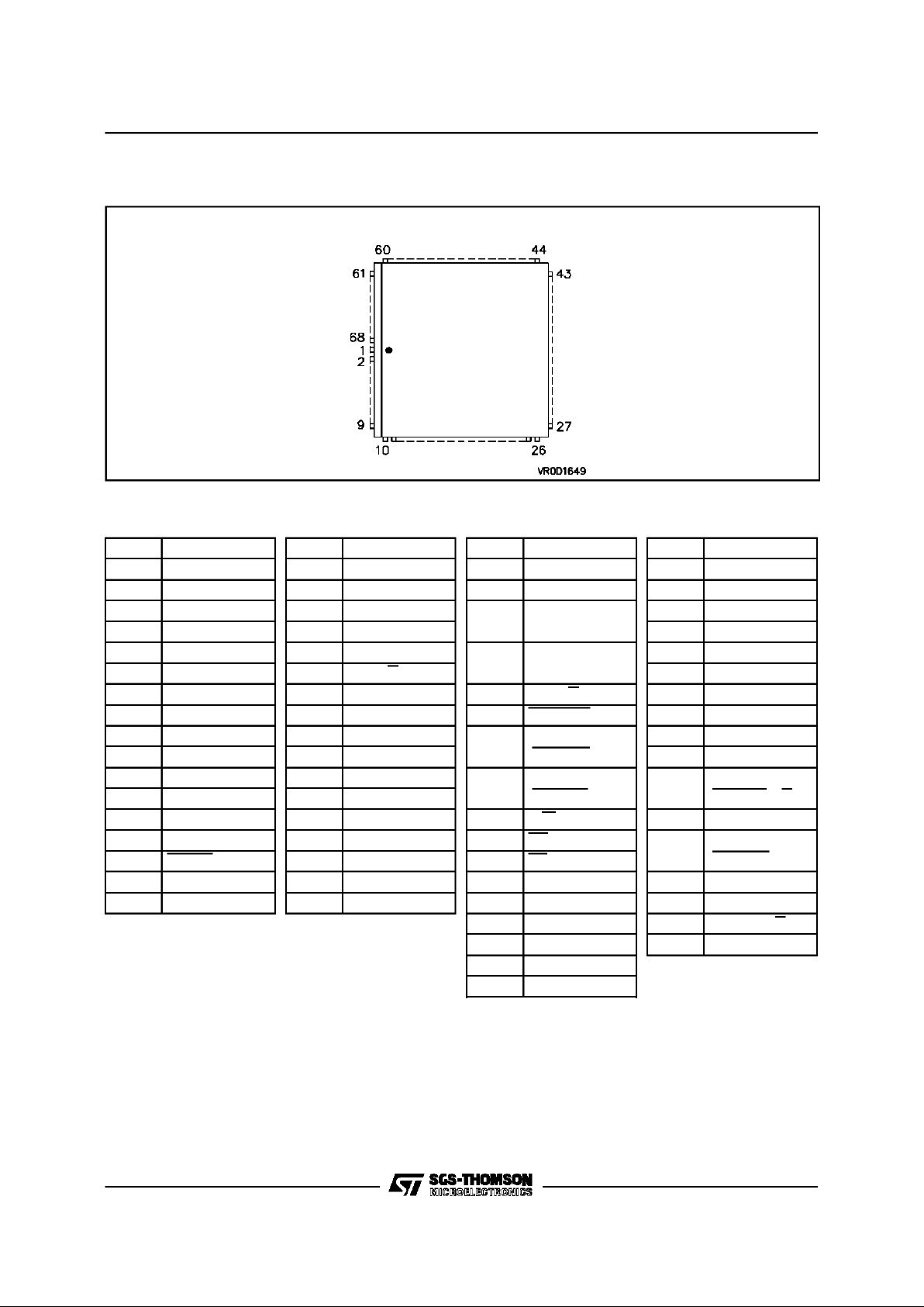
PQFP80
PLCC68
Registeroriented 8/16 bit COREwith
RUN,WFIandHALT modes
Minimuminstruction cycletime: 500ns
(12MHzinternal)
InternalMemory :
ROM 16K bytes
RAM 256 bytes
EEPROM 512 bytes
224generalpurposeregistersavailableasRAM,
accumulatorsorindexregisters(registerfile)
80-pin PQFPpackage forST9040Q
68-leadPLCCpackageforST9040C
DMA controller, Interrupthandler and SerialPe-
ripheralInterfaceas standardfeatures
Up to 56fullyprogrammable I/Opins
Up to 8 externalplus 1 non-maskableinterrupts
16 bit Timerwith 8 bit Prescaler,able to be used
as a WatchdogTimer
Two 16 bitMultifunction Timers, eachwith an8
bit prescalerand 13 operatingmodes
8 channel8 bit Analog to Digital Converter,with
AnalogWatchdogsandexternalreferences
Serial CommunicationsInterface with asynchro-
nous andsynchronouscapability
Rich InstructionSet and 14 Addressingmodes
Division-by-Zerotrap generation
Versatiledevelopmenttools,includingassembler,
linker, C-compiler, archiver, graphicoriented debuggerand hardwareemulators
Real TimeOperatingSystem
WindowedandOneTimeProgrammableEPROM
partsavailableforprototypingand pre-production
developmentphases
Pinto pincompatiblewith ST9036
1/56

TABLE OF CONTENTS
ST9040 ........................................ ..... 1
1.1GENERAL DESCRIPTION . . . . . . ........................ 5
1.2 PINDESCRIPTION . . . . . . . . . . ........................ 6
1.2.1 I/OPortAlternate Functions . . ....................... 6
1.3 MEMORY . . . . . ................................. 10
1.3.1 INTRODUCTION ............................... 10
1.3.2 EEPROM . .................................. 10
1.3.2.1 Introduction . . . . . . ........................ 10
1.3.2.2 EEPROM ProgrammingProcedure . . ................ 11
1.3.2.3 Parallel ProgrammingProcedure . . . ................ 11
1.3.2.4 EEPROM ProgrammingVoltage . . . ................ 11
1.3.2.5 EEPROM ProgrammingTime . . . . . . . .............. 11
1.3.2.6 EEPROM InterruptManagement . . . ................ 11
1.3.2.7 EEPROM ControlRegister ...................... 12
1.3.3 REGISTERMAP ............................... 12
2 ELECTRICAL CHARACTERISTICS .............................. 13
ST90E40/ ST90T40
................................... 35
1.1 GENERALDESCRIPTION . . . . . . ........................ 38
1.2 PINDESCRIPTION . . . . . . . . . . ........................ 39
1.2.1 I/OPORT ALTERNATEFUNCTIONS . . . . . . . . . . . . . . . . . . . . 39
1.1 MEMORY . . ..................................... 42
1.2 EPROMPROGRAMMING . . . . . . ........................ 42
1.2.1 EpromErasing ................................ 42
ST90R40
........................................ .... 49
1.1 GENERALDESCRIPTION . . . . . . ........................ 51
1.2 PINDESCRIPTION . . . . . . . . . . ........................ 52
1.2.1 I/OPORT ALTERNATEFUNCTIONS . . . . . . . . . . . . . . . ..... 52
1.3 MEMORY . . ..................................... 55
2/56

Figure1. 80 Pin PQFP Package
Pin Name Pin Name Pin Name Pin Name
1AV
SS
25 P34/T1INA 64 P20/NMI 80 AV
DD
2 NC 26 P33/T0OUTB 63 NC 79 NC
3 NC 27 P32/T0INB 62 V
SS
78 P47/AIN7
4 P44/AIN4 28 P31/T0OUTA 61 P70/SIN 77 P46/AIN6
5 P57 29 P30/P/D/T0INA 60 P71/SOUT 76 P45/AIN5
6 P56 30 A15
59
P72/INT4/TXCLK
/CLKOUT
75 P43/AIN3
7 P55 31 A14 74 P42/AIN2
8 P54 32 NC
58
P73/INT5
/RXCLK/ADTRG
73 P41/AIN1
9 INT7 33 A13 72 P40/AIN0
10 INT0 34 A12 57 P74/P/D/INT6 71 P27/RRDY5
11 P53 35 A11 56 P75/WAIT
70
P26/INT3
/RDSTB5/P/D
12 NC 36 A10
55
P76/WDOUT
/BUSREQ
13 P52 37 A9 69 P25/WRRDY5
14 P51 38 A8
54
P77/WDIN
/BUSACK
68
P24/INT1
/WRSTB5
15 P50 39 P00/A0/D0
16 OSCOUT 40 P01/A1/D1 53 R/W 67 P23/SDO
17 V
SS
52 NC 66 P22/INT2/SCK
18 V
SS
51 DS 65 P21/SDI/P/D
19 NC 50 AS
20 OSCIN 49 NC
21 RESET 48 V
DD
22 P37/T1OUTB 47 V
DD
23 P36/T1INB 46 P07/A7/D7
24 P35/T1OUTA 45 P06/A6/D6
44 P05/A5/D5
43 P04/A4/D4
42 P03/A3/D3
41 P02/A2/D2
Table 1. ST9040QPin Description
ST9040
3/56
Pin Name Pin Name Pin Name Pin Name
61 P44/AIN4 10 P35/T1OUTA 43 P70/SIN 60 AV
SS
62 P57 11 P34/T1INA 42 P71/SOUT 59 AV
DD
63 P56 12 P33/T0OUTB
41
P72/CLKOUT
/TXCLK/INT4
58 P47/AIN7
64 P55 13 P32/T0INB 57 P46/AIN6
65 P54 14 P31/T0OUTA
40
P73/ADTRG
/RXCLK/INT5
56 P45/AIN5
66 INT7 15 P30/P/D/T0INA 55 P43/AIN3
67 INT0 16 P17/A15 39 P74/P/D/INT6 54 P42/AIN2
68 P53 17 P16/A14 38 P75/WAIT 53 P41/AIN1
● 1 P52 18 P15/A13
37
P76/WDOUT
/BUSREQ
52 P40/AIN0
2 P51 19 P14/A12 51 P27/RRDY5
3 P50 20 P13/A11
36
P77/WDIN
/BUSACK
50
P26/INT3
/RDSTB5/P/D
4 OSCOUT 21 P12/A10
5V
SS
22 P11/A9 35 R/W 49 P25/WRRDY5
6 OSCIN 23 P10/A8 34 DS
48
P24/INT1
/WRSTB5
7 RESET 24 P00/A0/D0 33 AS
8 P37/T1OUTB 25 P01/A1/D1 32 V
DD
47 P23/SDO
9 P36/T1INB 26 P02/A2/D2 31 P07/A7/D7 46 P22/INT2/SCK
30 P06/A6/D6 45 P21/SDI/P/D
29 P05/A5/D5 44 P20/NMI
28 P04/A4/D4
27 P03/A3/D3
Table 2. ST9040C Pin Description
Figure2. 68 Pin PLCCPackage
ST9040
4/56

1.1GENERALDESCRIPTION
TheST9040isa ROMmemberof theST9 familyof
microcontrollers, completely developed and producedby SGS-THOMSONMicroelectronicsusing
a proprietaryn-well HCMOSprocess.
The ST9040 peripheraland functional actions are
fully compatible throughout the ST903x/4xfamily.
This datasheet will thus provide only information
specifictothis ROMdevice.
THE READER IS ASKED TO REFER TO THE
DATASHEET OFTHE ST9036ROM-BASEDDEVICEFORFURTHER DETAILS.
The nucleus of the ST9040 is the advanced Core
whichincludes the CentralProcessingUnit(CPU),
the Register File, a 16 bit Timer/Watchdog with 8
bitPrescaler,aSerialPeripheralInterfacesupportingS-bus,I
2
C-busand IM-busInterface,plustwo8
bit I/O ports. The Core has independent memory
and registerbuses allowing a high degree of pipeliningtoadd to theefficiencyof thecode execution
speedof the extensiveinstruction set.Thepowerful I/O capabilities demanded by microcontroller
applicationsare fulfilledby the ST9040 with up to
56 I/O lines dedicated to digital Input/Output.
These linesare grouped into up to seven 8 bit I/O
Ports and can be configured on a bit basis under
software control to provide timing, status signals,
an address/databus forinterfacing externalmemory,timer inputs and outputs,analoginputs,external interrupts and serial or parallel I/O with or
withouthandshake.
Threebasi cme mor yspac esare availableto support
this wide range of configurations: Program Memory
(internalandexter nal),DataMemor y(inter nalandexternal)andtheRegisterFile,whichincludesthecontrol
andstatusregis tersoftheon-c hi pperi pher als.
Two16 bit MultiFunctionTimers,each withan 8bit
Prescaler and 13 operating modes allow simple
use for complex waveform generation and measurement, PWM functions and many other system
timingfunctionsby theusageof thetwo associated
DMA channels for each timer. In addition there is
an8 channelAnalog to Digital Converterwith integral sample and hold, fast 11µs conversion time
and 8 bit resolution. An Analog Watchdog feature
isincludedfor two input channels.
Completingthe device is a full duplex Serial Communications Interface with an integral 110 to
375,000 baud rate generator, asynchronous and
1.5Mbyte/ssynchronous capability(fully programmable format) and associated address/wake-up
option,plustwo DMA channels.
ST9040
5/56

Figure3. ST9040 Block Diagram
1.2 PIN DESCRIPTION
AS.
Address Strobe (output, active low, 3-state).
Address Strobe is pulsed low once at the beginning of each memory cycle. The rising edge of AS
indicates that address, Read/Write (R/W), and
DataMemorysignalsare validforprogramor data
memorytransfers. Under programcontrol, AScan
be placed in a high-impedance state along with
Port0andPort 1, Data Strobe(DS) andR/W.
DS.
DataStrobe(output,activelow,3-state).
Data
Strobeprovidesthe timingfor datamovement toor
from Port 0 for each memory transfer. During a
writecycle, data out is valid at the leadingedgeof
DS
. Duringa readcycle,DataInmustbevalid prior
to the trailing edge of DS. When the ST9040 accesseson-chipmemory,DSis held highduringthe
wholememorycycle.It can be placed ina highimpedancestatealongwithPort0,Port1,ASandR/W.
R/W.
Read/Write (output, 3-state).
Read/Write
determines the direction of data transfer for external memory transactions. R/W is low when writing
to external program ordata memory, and high for
all othertransactions.Itcanbe placedin a high impedancestatealongwithPort0,Port1, ASandDS.
RESET.
Reset(input,active low).
TheST9isinitialisedby theResetsignal.WiththedeactivationofRESET, program execution begins from the Program
memorylocationpointedto by the vectorcontained
inprogrammemorylocations00hand01h.
INT0,INT7.Externalinterrupts(input,activeonrising or falling edge). Externalinterrupt inputs 0 and
7 respectively.INT0channelmay alsobe used for
the timerwatchdog interrupt.
OSCIN, OSCOUT
.
Oscillator (input and output).
These pins connect a parallel-resonant crystal
(24MHz maximum), or an external source to the
on-chipclockoscillatorand buffer.OSCINistheinput of the oscillatorinverterand internal clockgenerator; OSCOUT is the output of the oscillator
inverter.
AV
DD
. AnalogVDDoftheAnalogtoDigitalConverter.
AV
SS.
Analog VSSof the Analog to Digital Con-
verter.
MustbetiedtoV
SS
.
VDD. Main Power SupplyVoltage (5V± 10%)
V
SS
. DigitalCircuitGround.
P0.0-P0.7,P1.0-P1.7, P2.0-P2.7P3.0-P3.7, P4.0P4.7, P5.0-P5.7, P7.0-P7.7
I/O Port Lines (In-
put/Output, TTL or CMOS compatible)
. 56 lines
grouped into I/O ports of 8 bits, bit programmable
under program control as general purpose I/O or
as alternatefunctions.
1.2.1 I/O PortAlternate Functions
Each pin of the I/O ports of the ST9040 may assume software programmable Alternative Functions as shownin the Pin Configuration Drawings.
Table 1-3 shows the Functions allocated to each
I/OPort pinsand a summaryofpackagesforwhich
they are available.
CPU
16-Bit TIMER / WATCHDOG + SPI
SCI
WITH DMA
I/O PORT 7
(SCI)
8
256 Bytes
REGISTER FILE
2 x 16-bit TIMER
WITH DMA
I/O PORT 3
( TIMERS )
8
I/O PORT 0
(Address/Data)
8
I/O PORT 1
( Address )
8
512 B y t es
EEPROM
256 Bytes
RAM
16k Byt es
ROM
I/O PORT 2
( SPI )
8
I/O PORT 4
( Analog Inputs )
8
A/D
CONVERTER
I/O PORT 5
WITH HANDSHAKE
8
MEMORY BUS
REGISTER BUS
VR001385
INT0 INT7
AV
DDAVSS
ST9040
6/56

I/O PORT Name Function Alternate Function Pin Assignment
Port.bit PLCC PQFP
P0.0 A0/D0 I/O Address/Data bit 0mux 24 39
P0.1 A1/D1 I/O Address/Data bit 1mux 25 40
P0.2 A2/D2 I/O Address/Data bit 2mux 26 41
P0.3 A3/D3 I/O Address/Data bit 3mux 27 42
P0.4 A4/D4 I/O Address/Data bit 4mux 28 43
P0.5 A5/D5 I/O Address/Data bit 5mux 29 44
P0.6 A6/D6 I/O Address/Data bit 6mux 30 45
P0.7 A7/D7 I/O Address/Data bit 7mux 31 46
P1.0 A8 O Address bit8 23 38
P1.1 A9 O Address bit9 22 37
P1.2 A10 O Address bit10 21 36
P1.3 A11 O Address bit11 20 35
P1.4 A12 O Address bit12 19 34
P1.5 A13 O Address bit13 18 33
P1.6 A14 O Address bit14 17 31
P1.7 A15 O Address bit15 16 30
P2.0 NMI I Non-Maskable Interrupt 44 64
P2.0 ROMless I ROMless Select (Mask option) 44 64
P2.1 P/D O Program/DataSpace Select 45 65
P2.1 SDI I SPISerial Data Out 45 65
P2.2 INT2 I External Interrupt 2 46 66
P2.2 SCK O SPI SerialClock 46 66
P2.3 SDO O SPI Serial Data In 47 67
P2.4 INT1 I External Interrupt 1 48 68
P2.4 WRSTB5 I Handshake Write StrobeP5 48 68
P2.5 WRRDY5 O Handshake Write Ready P5 49 69
P2.6 INT3 I External Interrupt 3 50 70
P2.6 RDSTB5 I Handshake Read Strobe P5 50 70
P2.6 P/D O Program/Data Space Select 50 70
P2.7 RDRDY5 O Handshake Read Ready P5 51 71
P3.0 T0INA I MF Timer 0Input A 15 29
P3.0 P/D O Program/Data Space Select 15 29
P3.1 T0OUTA O MF Timer 0 Output A 14 28
P3.2 T0INB I MF Timer 0Input B 13 27
P3.3 T0OUTB O MF Timer 0 Output B 12 26
P3.4 T1INA I MF Timer 1Input A 11 25
Table 3. ST9040 I/O Port Alternate FunctionSummary
PINDESCRIPTION (Continued)
ST9040
7/56

I/O PORT Name Function Alternate Function Pin Assignment
Port.bit PLCC PQFP
P3.5 T1OUTA O MF Timer 1 Output A 10 24
P3.6 T1INB I MF Timer 1Input B 9 23
P3.7 T1OUTB O MF Timer 1 Output B 8 22
P4.0 AIN0 I A/D Analog Input 0 52 72
P4.1 AIN1 I A/D Analog Input 1 53 73
P4.2 AIN2 I A/D Analog Input 2 54 74
P4.3 AIN3 I A/D Analog Input 3 55 75
P4.4 AIN4 I A/D Analog Input 4 61 4
P4.5 AIN5 I A/D Analog Input 5 56 76
P4.6 AIN6 I A/D Analog Input 6 57 77
P4.7 AIN7 I A/D Analog Input 7 58 78
P5.0 I/O I/O Handshake Port 5 3 15
P5.1 I/O I/O Handshake Port 5 2 14
P5.2 I/O I/O Handshake Port 5 1 13
P5.3 I/O I/O Handshake Port 5 68 11
P5.4 I/O I/O Handshake Port 5 65 8
P5.5 I/O I/O Handshake Port 5 64 7
P5.6 I/O I/O Handshake Port 5 63 6
P5.7 I/O I/O Handshake Port 5 62 5
P7.0 SIN I SCISerial Input 43 61
P7.1 SOUT O SCI Serial Output 42 60
P7.1 ROMless I ROMless Select (Mask option) 42 60
P7.2 INT4 I External Interrupt 4 41 59
P7.2 TXCLK I SCI Transmit Clock Input 41 59
P7.2 CLKOUT O SCI Byte Sync Clock Output 41 59
P7.3 INT5 I External Interrupt 5 40 58
P7.3 RXCLK I SCI Receive Clock Input 40 58
P7.3 ADTRG I A/D Conversion Trigger 40 58
P7.4 INT6 I External Interrupt 6 39 57
P7.4 P/D O Program/Data Space Select 39 57
P7.5 WAIT I ExternalWait Input 38 56
P7.6 WDOUT O T/WD Output 37 55
P7.6 BUSREQ I External Bus Request 37 55
P7.7 WDIN I T/WD Input 36 54
P7.7 BUSACK O External Bus Acknowledge 36 54
Table 4. ST9040 I/O Port Alternate FunctionSummary(Continued)
PINDESCRIPTION
(Continued)
ST9040
8/56

Applicablefor ST9040
DEC
DEC
HEX
00
00
02
02
03
03
08
08
09
09
10
0A
24
18
63
3F
R255 RFF RESERVEDRESERVED
PORT 7
MFT 1
RESERVED
MFT 0
RESERVED
A/D
RFF
R254 RFE
MSPI
PORT 3
RFE
R253 RFD RFD
R252 RFC WCR RFC
R251 RFB
T/WD
RESERVED
RESERVED
RFB
R250 RFA
PORT 2
RFA
R249 RF9 RF9
R248 RF8 MFT RF8
R247 RF7
EXT INT
RESERVED
PORT 5 MFT 1
SCI RF7
R246 RF6
PORT1
RF6
R245 RF5 RF5
R244 RF4 RF4
R243 RF3 RESERVEDRESERVED
MFT0
RF3
R242 RF2
PORT 0 PORT 4
RF2
R241 RF1 EEPROMCR RF1
R240 RF0 RESERVED RF0
Table1-4. Group F PeripheralOrganization
ADDRESSSPACES
ST9040
9/56

Figure1-4. Memory Map
1.3 MEMORY
1.3.1 INTRODUCTION
Thememoryof the ST9isdivided into twospaces:
-
Data memory with up to64K (65536) bytes
-
Programmemory with up to 64K (65536) bytes
Thus,there isa totalof 128Kbytes of addressable
memoryspace.
The 16K bytes of on-chip ROM memory of the
ST9040 are selected at memory addresses 0
through 3FFFh (hexadecimal) in the PROGRAM
space.
TheDATAspaceincludesthe 512 bytesof on-chip
EEPROM at addresses 0 through 1FFh and the
256 bytes of on-chip RAM memory at addresses
200hthrough2FFh.
1.3.2 EEPROM
1.3.2.1 Introduction
TheEEPROMmemory providesuser-programmablenon-volatilememoryon-chip,allowing fast and
reliable storage of user data. As there is also no
off-chip access required, as for an external serial
EEPROM,high securitylevels can be achieved.
The EEPROM memory is read as normal RAM
memoryat DataSpace addresses0 to 1FFh, however one WAIT cycle is automatically added for a
Read cycle, while a byte write cycle to the
EEPROMwillcausethe startof anERASE/WRITE
cycle at the addressed location. Word (16 bit)
writesarenotallowed.
The programmingcycleis self-timed,withatypical
programmingtime of 6ms. The voltage necessary
for programmingthe EEPROMis internally generated with a +18Vcharge pump circuit.
Up to 16 bytes of data may be programmed into
the EEPROMduringthesame write cycleby using
the PARALLELWRITEfunction.
A standbymodeis alsoavailablewhichdisablesall
power consumption sources within the EEPROM
for low power requirements. When STBY is high,
any attempt to access the EEPROM memory will
produce unpredictable results. After the re-enabling of the EEPROM,a delay of 6 INTCLKcycles
must be allowed before the selection of the
EEPROM.
The EEPROM of the ST9040 has been implemented in a high reliability technology developed
by SGS-THOMSON,this,togetherwith the double
bit structure,allow300kErase/Writecyclesand10
year dataretention to be achieved on a microcontroller.
Controlof the EEPROM is performedthroughone
registermappedat registeraddressR241inPage0.
ST9040
10/56

1.3.2.2 EEPROMProgrammingProcedure
TheprogrammingofabyteofEEPROMmemory is
equivalentto writing a byte into a RAMlocation after verifying that EEBUSY bit is low. Instructions
operatingon worddata (16bits)willnot accessthe
EEPROM.
The EEPROM ENABLE bit EEWEN must first be
setbeforewriting to the EEPROM.When this bit is
low, attempts to write data to the EEPROM have
no affect, this prevents any spurious memory accessesfrom affectingthedatain the EEPROM.
Terminationof the writeoperation canbedetected
by polling on the EEBUSY status bit, or by interrupt, taking the interrupt vector from the External
Interrupt4 channel.Theselectionoftheinterruptis
made by EEPROM Interrupt enable bit EEIEN. It
shouldbe noted thattheMask bit of ExternalInterrupt 4 shouldbe set, and the InterruptPending bit
reset, before the setting of EEIEN to prevent unwanted interrupts. A delay (eg a nop instruction)
shouldalsobe includedbetween theoperationson
the maskand pendingbitsof ExternalInterrupt4.
If pollingon EEBUSYis used,a delayof 6 INTCLK
clockcyclesisnecessaryaftertheend of programming, this can be a nop instruction or, normally,
therequired time to test the EEBUSY bit and to
branch to the next instruction will be sufficient.
WhileEEBUSYisactive,anyattemptto accessthe
EEPROMmatrix will be aborted and the data read
will be invalid. EEBUSYis a read only bit and cannot bereset bythe user if active.
Anerasedbit of theEEPROMmemorywill read as
a logic“0”, while a programmedcell willberead as
a logic “1”. For applications requiring the highest
levelof reliability,theVerifyMode,set byEEPROM
controlregisterbit VRFY,allowsthe readingof the
EEPROM memory cells with a reduced gate voltage (typically 20%). If the EEPROM memory cell
hasbeen correctlyprogrammed, a logic “1” willbe
readwith thereduced voltage,otherwisealogic“0”
will beread.
1.3.2.3 ParallelProgrammingProcedure
Parallelprogramming is a featureof the EEPROM
macrocell. Oneup to sixteen bytes of a samerow
canbe programmedatonce.
Theconstraintisthateach ofthebytesoccurin the
sameROWof theEEPROMmemory (A4constant,
A3-A0variable).To operatethismode, the Parallel
Mode enable bit, PLLEN, must be set. The data
written is then latched into buffers (at the addresses specified, which may be non-sequential)
and then transferred to the EEPROM memory by
the setting of the PLLST bit of the control register.
Both PLLST and PLLEN are internally reset at the
end ofthe programmingcycle.Any attemptto read
the EEPROMmemorywhen PLLEN is set willgive
invaliddata.In the event that the data in the buffer
latchesisnot requiredtobewrittenintothememory
bythesettingofPLLST,thecorrectwaytoterminate
the operation is to reset PLLEN and to perform a
dummyreadoftheEEPROMmemory.Thisterminationwillclearalldata presentin thelatches.
1.3.2.4 EEPROMProgrammingVoltage
No external Vpp voltage is required, an internal
18Volt charge-pump gives the required energy by
a dedicated oscillator pumping at a typical frequencyof 5MHz,regardlessofthe external clock.
1.3.2.5 EEPROMProgrammingTime
No timing routine is required to control the programmingtime as dedicated circuitrytakescareof
the EEPROM programming time (The typical programmingtime is 6ms).
1.3.2.6 EEPROMInterruptManagement
At the end of each write procedure the EEPROM
sends aninterruptrequest(ifEEIEN bit isset). The
EEPROM sharesits interrupt channel with the externalinterruptsourceINT4,fromwhichthe priority
level is derived.
Care must be taken when EEIEN is reset.The associated external interrupt channel must be disabled (by reseting bit 4 of EIMR, R244) along with
reseting the interrupt pending bit (bit 4 of EIPR,
R243) to prevent unwanted interrupts.A delay instruction (at least 1
nop
instruction) must be in-
sertedbetweenthesetwo operations
WARNING.
The content of the EEPROM of the
ST9040 family after the out-going test at SGSTHOMSON’s manufacturing location is not guarenteed.
EEPROM
(Continued)
ST9040
11/56

Figure1-5. EEPROMParallel Programming Rows
EEPROM(Continued)
1.3.2.7 EEPROMControlRegister
EECR R241
(F1h) Page 0 Read/Write
(exceptEEBUSY:readonly)
EEPROMControl Register
Resetvalue : 0000 0000b(00h)
70
0 VERIFY EESTBY EEIEN PLLST PLLEN EEBUSYEEWEN
bit 7 = B7: This bit is forced to “0” after reset and
MUSTnotbe modifiedby the user.
bit 6 = VERIFY:
Set Verify mode
. Verify (active
high)is usedtoactivatethe verifymode.
The verify mode provides a guarenteeof good re-
tention of the programmed bit. When active, the
readingvoltageon the cell gate is decreasedfrom
1.2V to 0.0V, decreasing the current from the programmed cell by 20%. If the cell is well programmed(to “1”), a “1” will still be read, otherwise
a “0”will beread.
Note. Theverifymode mustnotbeused duringan
erasingor a programmingcycle).
bit 5 = EESTBY:
EEPROMStand-By
. EESTBY =
“1” switchesoff all power consumptionsources inside the EEPROM. Any attempt to access the
EEPROMwhen EESTBY= “1” will produce unpredictableresults.
Note.
AfterEESTBYisreset,the user must wait 6
CPUCLKcycles (e.g. 1 nop instruction)before selectingtheEEPROM.
bit 4 = EEIEN:
EEPROMInterruptEnable
. INTEN
= “1” disables the external interrupt source INT4,
and enablesthe EEPROM to send its interrupt requestto the centralinterruptunit at theend ofeach
write procedure.
bit 3 = PLLST:
ParallelWriteStart
. Setting PLLST
to“1”startstheparallel writingprocedure.It can be
setonlyifPLLENis alreadyset.PLLSTis internally
resetat the endof the programmingsequence.
bit 2 = PLLEN:
Parallel write Enable
. Setting
PLLEN to “1” enables the parallel writing mode
which allowsthe user to writeupto 16 bytesat the
same time. PLLEN is internallyreset at the end of
the programmingsequence.
bit 1 = EEBUSY:
BUSY
. When this read only bit is
high, an EEPROM write operation is in progress
and any attempt to access the EEPROM is
aborted.
bit 0 =
EEWEN:
EEPROM Write Enable
. Setting
this bitallowsprogramming ofthe EEPROM,when
low a writingattempthas no effect.
1.3.3 REGISTERMAP
Pleaserefer to the RegisterMap of the ST9036for
all generalregisterswiththe exceptionofthe register showninthe followingtable.
EECR
R241 (F1h) Page 0 Read/Write ControlRegisters
Table1-5. Register MapAddendum
ST9040
12/56

2 ELECTRICALCHARACTERISTICS
Symbol Parameter Value Unit
V
DD
Supply Voltage – 0.3to 7.0 V
AV
DD
,AV
SS
Analog Supply Voltage VSS=AVSS<AV
DD
≤
V
DD
V
V
I
Input Voltage – 0.3 to VDD+0.3 V
V
O
Output Voltage – 0.3 to VDD+0.3 V
T
STG
Storage Temperature – 55 to +150
°
C
I
INJ
Pin Injection Current DigitalInput -5 to +5 mA
I
INJ
Pin Injection Current AnalogInput -5 to +5 mA
Maximum Accumulated Pin injection Current in thedevice -50 to +50 mA
Note
:Stresses abovethose listedas “absolutemaximumratings” may cause permanent damage to the device. This is a stressrating onlyand
functional operation of the device at these conditions is not implied. Exposure to maximum rating conditions for extended periods may affect
device reliability.Allvoltages are referenced toV
SS
ABSOLUTEMAXIMUM RATINGS
Symbol Parameter
Value
Unit
Min. Max.
T
A
Operating Temperature – 40 85 °C
V
DD
Operating Supply Voltage 4.5 5.5 V
f
OSCE
External OscillatorFrequency 24 MHz
f
OSCI
Internal Clock Frequency (INTCLK) 12 MHz
RECOMMENDED OPERATING CONDITIONS
ST9040
13/56

Symbol Parameter Test Conditions
Value
Unit
Min. Typ. Max.
V
IHCK
Clock Input High Level External Clock 0.7 V
DD
VDD+ 0.3 V
V
ILCK
Clock Input Low Level External Clock – 0.3 0.3 V
DD
V
V
IH
Input High Level
TTL 2.0 V
DD
+ 0.3 V
CMOS 0.7 V
DD
VDD+ 0.3 V
V
IL
Input Low Level
TTL – 0.3 0.8 V
CMOS – 0.3 0.3 V
DD
V
V
IHRS
RESET Input High Level 0.7 V
DD
VDD+ 0.3 V
V
ILRS
RESET Input Low Level –0.3 0.3 V
DD
V
V
HYRS
RESET Input Hysteresis 0.3 1.5 V
V
OH
Output High Level Push Pull,Iload = – 0.8mA VDD– 0.8 V
V
OL
Output Low Level
Push Pull or Open Drain,
Iload = 1.6mA
0.4 V
I
WPU
Weak Pull-up Current Bidirectional Weak Pull-
up, V
OL
=0V
– 50 – 200 – 420
µ
A
I
APU
Active Pull-up Current,
for INT0 and INT7 only
V
IN
< 0.8V, underReset – 80 – 200 –420
µ
A
I
LKIO
I/O Pin Input Leakage
Input/Tri-State,
0V < V
IN<VDD
–10 +10 µA
I
LKRS
Reset Pin Input Leakage 0V < VIN<V
DD
–30 +30 µA
I
LKAD
A/D Pin Input Leakage
Alternate Function,
Open Drain,
0V < V
IN<VDD
–3 +3 µA
I
LKAP
Active Pull-up Input
Leakage
0V < V
IN
<0.8V – 10 + 10 µA
I
LKOS
OSCIN Pin Input Leakage 0V < VIN<V
DD
–10 +10 µA
Note: AllI/OPorts are configured in Bidirectional Weak Pull-upMode with no DC load, ExternalClock pin (OSCIN) is driven by square wave
external clock. No peripheral working.
DC ELECTRICALCHARACTERISTICS
V
DD
=5V±10%TA=–40°Cto+85°C, unlessotherwisespecified)
DC TEST CONDITIONS
ST9040
14/56

Symbol Parameter Test Conditions
Value
Unit
Min. Typ. Max.
I
DD
Run Mode Current
no CPUCLK prescale,
Clock divide by 2
24MHz, Note 1 40 mA
I
DP2
Run Mode Current
Prescale by 2
Clock divide by 2
24MHz, Note 1 30 mA
I
WFI
WFIMode Current
no CPUCLK prescale,
Clock divide by 2
24MHz, Note 1 20 mA
I
HALT
HALT Mode Current 24MHz, Note 1 100
µ
A
Note 1: All I/OPortsare configured in Bidirectional Weak Pull-up Modewith no DC load, External Clock pin (OSCIN) is driven by squarewave
external clock. No peripheral working.
AC ELECTRICALCHARACTERISTICS
(V
DD
=5V±10%TA=–40°Cto+85°C, unless otherwise specified)
ST9040
15/56

N° Symbol Parameter
Value
Unit Note
Min. Max.
1 TpC OSCIN Clock Period
41.5 ns 1
83 ns 2
2 TrC, TfC OSCIN Rise and FallTime 12 ns
3 TwCL, TwCH OSCINLow and High Width
17 25 ns 1
38 ns 2
Notes:
1. Clock dividedby 2 internally (MODER.DIV2=1)
2. Clock notdivided by 2 internally(MODER.DIV2=0)
CLOCK TIMING TABLE
(V
DD
=5V
±
10%,T
A
=–40°Cto+85°C, INTCLK= 12MHz, unless otherwisespecified)
CLOCK TIMING
ST9040
16/56

N° Symbol Parameter
Value
(Note)
Unit
OSCIN Divided
By 2
OSCIN Not Divided
By 2
Min. Max.
1 TsA (AS)
Address Set-up Time
before AS ↑
TpC (2P+1) –22 TWCH+PTpC–18 20 ns
2 ThAS (A) AddressHoldTimeafterAS ↑ TpC –17 TwCL –13 25 ns
3 TdAS (DR) AS↑ toDataAvailable(read) TpC (4P+2W+4) –52 TpC (2P+W+2) –51 115 ns
4 TwAS AS Low Pulse Width TpC (2P+1) –7 TwCH+PTpC –3 35 ns
5 TdAz (DS) Address Float to DS ↓ t12 12 12ns
6 TwDSR DS Low Pulse Width (read) TpC (4P+2W+3) –20
TwCH+TpC
(2P+W+1) –16
105 ns
7 TwDSW DS Low Pulse Width (write) TpC (2P+2W+2) –13 TpC (P+W+1) –13 70 ns
8 TdDSR (DR) DS↓toDataValidDelay(read) TpC (4P+2W-3) –50
TwCH+TpC(2P+W+1)
–46
75 ns
9 ThDR (DS) DatatoDS ↑ HoldTime(read) 0 0 0 ns
10 TdDS (A) DS ↑ to Address Active Delay TpC –7 TwCL –3 35 ns
11 TdDS (AS) DS ↑ to AS ↓ Delay TpC –18 TwCL –14 24 ns
12 TsR/W (AS) R/W Set-upTimebeforeAS ↑ TpC (2P+1)–22 TwCH+PTpC –18 20 ns
13 TdDSR (R/W)
DS↑to R/W and AddressNot
Valid Delay
TpC –9 TwCL –5 33 ns
14 TdDW (DSW)
Write Data Valid to DS ↓ Delay
(write)
TpC (2P+1) –32 TwCH+PTpC –28 10 ns
15 ThDS (DW) Data Hold Time after DS ↑ (write) TpC –9 TwCL –5 33 ns
16 TdA (DR)
Address Valid to Data Valid
Delay (read)
TpC (6P+2W+5) –68
TwCH+TpC
(3P+W+2) –64
140 ns
17 TdAs (DS) AS↑ to DS ↓ Delay TpC –18 TwCL –14 24 ns
EXTERNALBUS TIMING TABLE
(V
DD
=5V±10%,TA=– 40 °Cto+85°C, Cload= 50pF,CPUCLK = 12MHz, unlessotherwisespecified)
EXTERNALWAIT TIMING TABLE
(V
DD
=5V±10%,TA=–40°Cto+85°C, Cload=50pF,
INTCLK=12MHz, Push-pulloutput configuration,unless otherwise specified)
N
°
Symbol Parameter
Value (Note)
Unit
OSCIN Divided
By 2
OSCIN Not Divided
By 2
Min. Max.
1 TdAs (WAIT) AS ↑ to WAIT ↓ Delay 2(P+1)TpC –29 2(P+1)TpC –29 40 ns
2 TdAs (WAIT) AS ↑ to WAIT ↓ Min. Delay 2(P+W+1)TpC –4 2(P+W+1)TpC –4 80 ns
3 TdAs (WAIT) AS ↑ to WAIT ↓ Max. Delay 2(P+W+1)TpC –29 2(P+W+1)TpC –29
83W+
40
ns
Note: (for both tables) The value in theleft hand two columns show the formula used to calculate the timingminimum or maximum from the
oscillator clock period, prescale value and number of wait cyclesinserted.
The value in theright handtwo columns show thetiming minimum andmaximum foran external clock at 24 MHz dividedby 2, prescaler value
of zero and zero wait status.
Legend: TpC =OSCIN Period
P = Clock Prescaling Value TwCH =HighLevel OSCINhalf period
W =Wait Cycles TwCL =Low Level OSCINhalfperiod
ST9040
17/56

EXTERNALBUS TIMING
EXTERNALWAIT TIMING
ST9040
18/56

N° Symbol Parameter
Value
(Note)
Min. Max. Unit
OSCIN Divided
By 2
OSCIN Not Divided
By 2
Min. Max. Min. Max.
1 TwRDY
RDRDY, WRRDY Pulse
Width inOne Line
Handshake
2TpC
(P+W+1)–18
TpC
(P+W+1) –
18
65 ns
2 TwSTB
RDSTB, WRSTB Pulse
Width
2TpC+12 TpC+12 95 ns
3
TdST
(RDY)
RDSTB, or WRSTB ↑
to RDRDY or WRRDY ↓
TpC+45
(TpC-TwCL)
+45
87 ns
4
TsPD
(RDY)
Port Data toRDRDY ↑
Set-upTime
(2P+2W+1)
TpC –25
TwCH+
(W+P)
TpC –25
16 ns
5
TsPD
(RDY)
Port Data toWRRDY
↓
Set-upTime in One Line
Handshake
43 43 43 ns
6
ThPD
(RDY)
Port Data toWRRDY
↓
Hold
Time in OneLine
Handshake
000ns
7
TsPD
(STB)
Port Data to WRSTB ↑
Set-upTime
10 10 10 ns
8
ThPD
(STB)
Port Data to WRSTB ↑
Hold Time
25 25 25 ns
9
TdSTB
(PD)
RDSTBD↑to Port Data
Delay Time in
BidirectionalHandshake
35 35 35 ns
10
TdSTB
(PHZ)
RDSTB ↑ to Port High-Z
Delay Time in
BidirectionalHandshake
25 25 25 ns
Note: The valuein the left hand two columns show the formula used to calculate the timing minimum or maximum from the oscillator clock
period,prescale value and number of wait cycles inserted.
The value in theright handtwo columns show thetiming minimum andmaximum foran external clock at 24 MHz dividedby 2, prescaler value
of zero and zero wait status.
Legend:
P = Clock PrescalingValue (R235.4,3,2)
W = Programmable Wait Cycles (R252.2.1.0/5,4,3) + ExternalWaitCycles
HANDSHAKE TIMING TABLE
(V
DD
=5V±10%,TA=–40°Cto+85°C, Cload= 50pF,INTCLK= 12MHz,
Push-pulloutputconfiguration,unlessotherwise specified)
ST9040
19/56

HANDSHAKETIMING
ST9040
20/56

N° Symbol Parameter
Value (Note)
Unit
OSCIN Divided
By 2
OSCIN NotDivided
By 2
Min. Max.
1 TdBR (BACK) BREQ↓to BUSACK
↓
TpC+8 TwCL+12 50 ns
TpC(6P+2W+7)+65 TpC(3P+W+3)+TwCL+65 360 ns
2 TdBR (BACK) BREQ↑to BUSACK
↑
3TpC+60 TpC+TwCL+60 185 ns
3 TdBACK (BREL)
BUSACK ↓ toBus
Release
20 20 20 ns
4 TdBACK (BACT)
BUSACK ↑ to Bus
Active
20 20 20 ns
Note: The value left hand two columns show the formula used tocalculate the timing minimum or maximum fromthe oscillator clock period,
prescale value and numberof wait cycles inserted.
The value right handtwocolumns show the timing minimum and maximum for an externalclock at 24MHz divided by 2, prescale value of zero
and zero waitstatus.
BUS REQUEST/ACKNOWLEDGE TIMING TABLE(VDD=5V±10%,TA=–40°Cto+85°C,Cload=50pF,
INTCLK=12MHz, Push-pulloutput configuration,unless otherwise specified)
Note :MEMINT = Group of memory interface signals: AS,DS, R/W,P00-P07,P10-P17
BUS REQUEST/ACKNOWLEDGE TIMING
ST9040
21/56

N° Symbol Parameter
Value (Note)
Unit
OSCIN
Divided By
2 Min.
OSCIN Not
Divided By
2 Min.
Min. Max.
1 TwLR Low LevelMinimum Pulse Width in Rising Edge Mode 2TpC+12 TpC+12 95 ns
2 TwHR High Level Minimum Pulse Width inRising Edge Mode 2TpC+12 TpC+12 95 ns
3 TwHF High Level Minimum Pulse Width inFalling Edge Mode 2TpC+12 TpC+12 95 ns
4 TwLF Low Level Minimum Pulse Width in Falling Edge Mode 2TpC+12 TpC+12 95 ns
Note: The value lefthand two columns show the formula used to calculate the timing minimum or maximum fromthe oscillatorclock period,
prescalevalue and number of wait cycles inserted.
The value righthand two columns show thetiming minimumandmaximum foran external clock at 24 MHzdivided by2,prescale value of zero
andzero waitstatus.
EXTERNALINTERRUPT TIMING TABLE
(V
DD
=5V±10%,TA=–40°Cto+85°C,Cload=50pF,
INTCLK= 12MHz,Push-pulloutput configuration,unlessotherwisespecified)
EXTERNALINTERRUPT TIMING
ST9040
22/56

N° Symbol Parameter
Value
Unit
Min. Max.
1 TsDI Input Data Set-upTime 100 ns
2 ThDI (1) Input Data Hold Time 1/2 TpC+100 ns
3 TdOV SCK to Output Data Valid 100 ns
4 ThDO Output Data Hold Time -20 ns
5 TwSKL SCK Low Pulse Width 300 ns
6 TwSKH SCK High Pulse Width 300 ns
Note: TpCis the OSCIN Clock period.
SPI TIMING TABLE (VDD=5V±10%,TA= –40°C to +85°C, Cload = 50pF, INTCLK = 12MHz,
OutputAlternate Functionset as Push-pull)
SPI TIMING
ST9040
23/56

WATCHDOG TIMING
N° Symbol Parameter
Values
Unit
Min. Max.
1 TwWDOL WDOUTLow Pulse Width 620 ns
2 TwWDOH WDOUT High Pulse Width 620 ns
3 TwWDIL WDIN High Pulse Width 350 ns
4 TwWDIH WDIN Low Pulse Width 350 ns
WATCHDOG TIMING TABLE(VDD=5V±10%,TA=–40°Cto+85°C,Cload= 50pF,
CPUCLK= 12MHz,Push-pulloutputconfiguration,unlessotherwisespecified)
ST9040
24/56

N° Symbol Parameter
Oscin divided
by 2
(1)
Oscin not
divided
(1)
Value
(2)
Unit
Min. Max. Min. Max. Min. Max.
1T
LOW
External Trigger pulse width 2xT
PC
T
PC
83 ns
2T
HIGH
External Trigger pulse 2xT
PC
T
PC
83 ns
3T
EXT
External trigger active
edges distance
138xT
PC
69xT
PC
5.75 µs
4T
STR
Internal delaybetween
EXTRG falling edge and first
conversion start
T
PC
3xTPC0.5xTPC 1.5xT
PC
41.5 125 ns
Notes:
1. Variable clock (TPC=OSCIN clock period)
2. INTCLK=12MHz
EXTERNAL TRIGGER TIMING(VDD=5V±10%, TA= –40°C to +85°C, Cload = 50pF)
A/D External TriggerTiming
A/D CONVERTER
ST9040
25/56

N° Symbol Parameter
OSCIN
Divided by 2 (2)
OSCIN
Not Divided by 2 (2)
Value (3)
Unit
Min. Max. Min. Max. Min. Max.
1Tw
HIGH
Internal trigger
pulse width
Tpc .5 x Tpc 41.5 - ns
2Tw
LOW
Internal trigger
pulse distance
6 x Tpc 3 x Tpc 250 - ns
3Tw
EXT
Internal trigger
active edges
distance (1)
276n x Tpc 138n x Tpc n x 11.5 -
µ
s
4Tw
STR
Internal delay
between INTRG
rising edge and
first conversion
start
Tpc 3 x Tpc .5 x Tpc 1.5 x Tpc 41.5 125 ns
A/D INTERNAL TRIGGER TIMING TABLE
A/D INTERNALTRIGGERTIMING
ST9040
26/56

N° Symbol Parameter
OSCIN
Divided by 2 (2)
OSCIN
Not Divided by 2 (2)
Value (3)
Unit
Min. Max. Min. Max. Min. Max.
1Tw
EXT
CEn Pulse width
(1)
276n x Tpc 138n x Tpc n x 11.5 - µs
Notes:
1. n = number ofautoscanned channels (1 < n < 8)
2. Variable clock (Tpc = OSCIN clock period)
3. CPUCLK =12MHz
A/D CHANNEL ENABLE TIMING TABLE
A/D CHANNEL ENABLETIMING
ST9040
27/56

Parameter Typical (1) Minimum Maximum Units (2) Notes
Analog Input Range
A
VCC
3
A
VCC
V
CC
V
Conversion time 11.5
µ
s (3, 4)
Sample time 3 µs (3)
Power-up time 60
µ
s
Resolution 8 8 βιτσ
Monotonicity GUARANTEED
No missing codes GUARANTEED
Zero input reading 00 Hex
Full scale reading FF Hex
Offset error .5 1 LSBs (2,6)
Gain error .5 1 LSBs (6)
Diff. Non Linearity
±
.3
±
.2
±
.5 LSBs (6)
Int. Non Linearity 1 LSBs (6)
Absolute Accuracy 1 LSBs (6)
S/N 45 49 dB
A
VCC/AVSS
Resistance 13.5 16 11 K
Ω
Input Resistance 12 8 15 KΩ (5)
Hold Capacitance 30 pF
Input Leakage ±3 µA
Notes:
1. The values are expectedat 25degree Centigradewith A
VCC
=5V
2. “LSBs”, as used here, has avalue of A
VCC
/256
3. @ 12MHz internal clock
4. Including sample time
5. It mustbe intendedas the internalseries resistance before thesampling capacitor
6. This is atypicalexpected value, butnota testedproduction parameter.
If V(i)is the valueof thei-th transition level (0 < i< 254), the performance of theA/D converter hasbeen valued as follows:
OFFSET ERROR= deviation between the actual V(0)and the ideal V(0) (=1/2 LSB)
GAIN ERROR= deviation between theactual V(254) and the ideal V(254) (=AVCC-3/2LSB)
DNL ERROR= max {[V(i) - V(i-1)]/LSB - 1}
INL ERROR= max {[V(i)- V(0)]/LSB -i}
A/D ANALOG SPECIFICATIONS
ST9040
28/56

MULTIFUNCTION TIMER UNIT EXTERNALTIMING
N° Symbol Parameter
OSCIN
Divided
by 2
(3)
OSCIN
Not
Divided
by 2
(3)
Value (4)
Unit Note
Min. Max.
1Tw
CTW
External clock/trigger pulse width 2n x Tpc n x Tpc n x 83 - ns 1
2Tw
CTD
External clock/trigger pulse distance 2n x Tpc n x Tpc n x 83 - ns 1
3Tw
AED
Distance between two active edges 6 x Tpc 3 x Tpc 249 - ns
4Tw
GW
Gate pulse width 12 x Tpc 6 x Tpc 498 - ns
5Tw
LBA
Distance between TINB pulse edge and
the following TINA pulse edge
2 x Tpc Tpc 83 - ns 2
6Tw
LAB
Distance between TINA pulse edge and
the following TINB pulse edge
00-ns2
7TwADDistance between two TxINApulses 0 0 - ns 2
8Tw
OWD
Minimum output pulse width/distance 6 x Tpc 3 x Tpc 249 - ns
Notes:
2.In Autodiscriminationmode
1. n = 1 ifthe input is risingORfalling edge sensitive 3.Variable clock ( Tpc = OSCIN period )
n = 3 if theinput is rising ANDfalling edge sensitive 4.INTCLK = 12 MHz
MULTIFUNCTION TIMER UNIT EXTERNALTIMING TABLE
ST9040
29/56

N°Symbol Parameter Condition
Value
Unit
Min. Max.
F
RxCKIN
Frequency of RxCKIN
1 x mode F
CK
/8 Hz
16 x mode F
CK
/4 Hz
Tw
RxCKIN
RxCKIN shortest pulse
1 x mode 4 T
CK
s
16 x mode 2 T
CK
s
F
TxCKIN
Frequency of TxCKIN
1 x mode F
CK
/8 Hz
16 x mode F
CK
/4 Hz
Tw
TxCKIN
TxCKIN shortest pulse
1 x mode 4 T
CK
s
16 x mode 2 T
CK
s
1Ts
DS
DS (Data Stable) beforerising
edge of RxCKIN
1 x mode receptionwith RxCKIN T
PC
/2 ns
2Td
D1
TxCKIN to Data out delay Time
1 x mode transmissionwith
external clock C load<100pF
2.5 T
PC
ns
3Td
D2
CLKOUT to Data out delay Time
1 x mode transmissionwith
CLKOUT
350 ns
Note: FCK= 1/T
CK
SCI TIMING TABLE
(V
DD
=5V±10%, TA=-40°C to+85°C,Cload = 50pF, INTCLK = 12MHz,
Output AlternateFunction set as Push-pull)
SCI TIMING
ST9040
30/56

80-Pin PlasticQuad Flat Package
PACKAGEMECHANICAL DATA
Dim. mm inches
Min Typ Max Min Typ Max
A 3.40 0.134
A2 2.55 2.80 3.05 0.100 0.110 0.120
D 22.95 23.20 24.45 0.903 0.913 0.923
D1 19.90 20.00 20.10 0.783 0.787 0.791
D3 18.40 0.724
E 16.95 17.20 17.45 0.667 0.677 0.687
E1 13.90 14.00 14.10 0.547 0.551 0.555
E3 12.00 0.472
e 0.80 0.032
Number of Pins
N80
ND 24
NE 16
ShortFootprint Measurement
Short Footprint recommendedPadding
ST9040
31/56

Sales Type Frequency Temperature Range Package
ST9040Q1/XX
24MHz
0°Cto + 70°C
PQFP80
ST9040C1/XX PLCC68
ST9040C6/XX -40°Cto+85°C PLCC68
Note:
”XX”is theROM code identifierthat is allocated by SGS-THOMSON after receipt of allrequired options and the related ROM file.
ORDERINGINFORMATION
68-Pin PlasticLeadlessChip Carrier
Dim. mm inches
Min Typ Max Min Typ Max
A 4.20 5.08 0.165 0.200
A1 0.51 0.020
A3 2.29 3.30 0.090 0.130
B-----B1------
D 25.02 25.27 0.985 0.995
D1 24.13 24.33 0.950 0.958
D3 20.32 0.800
E 25.02 25.27 0.985 0.995
E1 24.13 24.33 0.950 0.958
E3 20.32 0.800
K1------
h
e 1.27 0.050
Numberof Pins
N68
ND 16
NE 16
ST9040
32/56

ST9040STANDARD OPTIONLIST
Pleasecopy this page(enlargeif possible)and completeALLsections.
Sendtheform, with the ROM codeimage required,toyourlocalSGS-THOMSONsales office.
CustomerCompany : [
.................................................. ................
]
CompanyAddress : [
.................................................. ................
]
[
.................................................. ................
]
Telephone: [
............ ..............
]
FAX: [
............ ..............
]
Contact: [
............ ..............
] Telephone(Direct) : [
.............. ............
]
Pleaseconfirmcharacteristicsof device:
Device ST9040
Package [ ] PQFP80 [ ] PLCC68
TemperatureRange [ ] -40°Cto +85°C[]0°Cto+70°C
SpecialMarking [ ] No
[ ] Yes 14characters [ | | | | | ||||||||]
Authorizedcharactersare letters, digits,’.’,’-’, ’/’ andspaces only.
Pleaseconsult yourlocalSGS-THOMSONsales officeforothermarking detailsif required.
Notes:
Code : [ ] EPROM(27128, 27256)
[ ] HEXformat filesonIBM-PCcompatibledisk
filename: [
.............. ........
]
Confirmation : [ ] Codecheckedwith EPROMdevice in application
YearlyQuantityforecast : [
...........................
] k units
- fora periodof : [
...........................
] years
PreferredProductionstart dates : [
..................... ..
] (YY/MM/DD)
CustomerSignature :
Date:
ST9040
33/56

NOTES:
ST9040
34/56

ST90E40
ST90T40
16K EPROM HCMOS MCU
WITH EEPROM, RAM AND A/D CONVERTER
(Ordering Information at the end of the Datasheet)
PQFP80
PLCC68
Registeroriented 8/16 bit COREwith
RUN,WFIandHALT modes
Minimuminstruction cycletime:500ns
(12MHzinternal)
InternalMemory :
EPROM 16Kbytes
RAM 256 bytes
EEPROM 512 bytes
224 generalpurpose registersavailable as
RAM,accumulatorsor indexpointers
(RegisterFile)
80-pin Plastic Quad Flat Pack package for
ST90T40Q
68-leadPlasticLeaded Chip Carrierpackage for
ST90T40C
80-pin Windowed Ceramic Quad Flat Pack
package for ST90E40G
68-leadWindowedCeramicLeadedChipCarrier
packagefor ST90E40L
DMA controller, Interrupthandler and Serial PeripheralInterfaceas standardfeatures
56 fully programmableI/Opins
Up to 8 externalplus 1 non-maskableinterrupts
16 bit Timerwith 8 bit Prescaler,able to be used
as a WatchdogTimer
Two 16 bit Multifunction Timers, eachwith an8
bit prescalerand 13 operatingmodes
8 channel8 bit Analog to Digital Converter,with
AnalogWatchdogsandexternalreferences
Serial CommunicationsInterface with asynchro-
nous andsynchronouscapability
Rich InstructionSet and 14 Addressingmodes
Division-by-Zerotrap generation
VersatileDevelopmenttools,includingassembler,
linker, C-compiler, archiver, graphicoriented debuggerand hardwareemulators
Real TimeOperatingSystem
Compatiblewith ST9036and ST9040 16K ROM
devices
CQFP80W
March 1994
CLCC68W
35/56

Figure1. 80 Pin QFP Package
Pin Name Pin Name Pin Name Pin Name
1AV
SS
25 P34/T1INA 64 P20/NMI 80 AV
DD
2 NC 26 P33/T0OUTB 63 NC 79 NC
3 NC 27 P32/T0INB 62 V
SS
78 P47/AIN7
4 P44/AIN4 28 P31/T0OUTA 61 P70/SIN 77 P46/AIN6
5 P57 29 P30/P/D/T0INA 60 P71/SOUT 76 P45/AIN5
6 P56 30 P17/A15
59
P72/INT4/TXCLK
/CLKOUT
75 P43/AIN3
7 P55 31 P16/A14 74 P42/AIN2
8 P54 32 NC
58
P73/INT5
/RXCLK/ADTRG
73 P41/AIN1
9 INT7 33 P15/A13 72 P40/AIN0
10 INT0 34 P14/A12 57 P74/P/D/INT6 71 P27/RRDY5
11 P53 35 P13/A11 56 P75/WAIT
70
P26/INT3
/RDSTB5/P/D
12 NC 36 P12/A10
55
P76/WDOUT
/BUSREQ
13 P52 37 P11/A9 69 P25/WRRDY5
14 P51 38 P10/A8
54
P77/WDIN
/BUSACK
68
P24/INT1
/WRSTB5
15 P50 39 P00/A0/D0
16 OSCOUT 40 P01/A1/D1 53 R/W 67 P23/SDO
17 V
SS
52 NC 66 P22/INT2/SCK
18 V
SS
51 DS 65 P21/SDI/P/D
19 NC 50 AS
20 OSCIN 49 NC
21 RESET/V
PP
48 V
DD
22 P37/T1OUTB 47 V
DD
23 P36/T1INB 46 P07/A7/D7
24 P35/T1OUTA 45 P06/A6/D6
44 P05/A5/D5
43 P04/A4/D4
42 P03/A3/D3
41 P02/A2/D2
Table 1. ST90E40G-ST90T40QPin Description
ST90E40 - ST90T40
36/56

Pin Name Pin Name Pin Name Pin Name
61 P44/AIN4 10 P35/T1OUTA 43 P70/SIN 60 AV
SS
62 P57 11 P34/T1INA 42 P71/SOUT 59 AV
DD
63 P56 12 P33/T0OUTB
41
P72/CLKOUT
/TXCLK/INT4
58 P47/AIN7
64 P55 13 P32/T0INB 57 P46/AIN6
65 P54 14 P31/T0OUTA
40
P73/ADTRG
/RXCLK/INT5
56 P45/AIN5
66 INT7 15 P30/P/D/T0INA 55 P43/AIN3
67 INT0 16 P17/A15 39 P74/P/D/INT6 54 P42/AIN2
68 P53 17 P16/A14 38 P75/WAIT 53 P41/AIN1
● 1 P52 18 P15/A13
37
P76/WDOUT
/BUSREQ
52 P40/AIN0
2 P51 19 P14/A12 51 P27/RRDY5
3 P50 20 P13/A11
36
P77/WDIN
/BUSACK
50
P26/INT3
/RDSTB5/P/D
4 OSCOUT 21 P12/A10
5V
SS
22 P11/A9 35 R/W 49 P25/WRRDY5
6 OSCIN 23 P10/A8 34 DS
48
P24/INT1
/WRSTB5
7 RESET/V
PP
24 P00/A0/D0 33 AS
8 P37/T1OUTB 25 P01/A1/D1 32 V
DD
47 P23/SDO
9 P36/T1INB 26 P02/A2/D2 31 P07/A7/D7 46 P22/INT2/SCK
30 P06/A6/D6 45 P21/SDI/P/D
29 P05/A5/D5 44 P20/NMI
28 P04/A4/D4
27 P03/A3/D3
Table 2. ST90E40L-ST90T40C
Figure2. 68 Pin LCC Package
ST90E40- ST90T40
37/56

Figure3. ST90E40 Block Diagram
1.1 GENERALDESCRIPTION
The ST90E40 and ST90T40 (following mentioned
asST90E40)areEPROMmembers oftheST9familyofmicrocontrollers,in windowedceramic(E) and
plasticOTP(T) packages respectively,completely
developed and produced by SGS-THOMSONMicroelectronics using a n-well proprietary HCMOS
process.
The EPROM parts are fully compatible with their
ROMversionsand this datasheet will thus provide
onlyinformationspecific to the EPROM baseddevices.
THE READER IS ASKED TO REFER TO THE
DATASHEET OFTHEST9040 ROM-BASED DEVICEFORFURTHERDETAILS.
The EPROMST90E40may be usedfor the prototypingand pre-productionphasesof development,
and can be configuredas: a standalonemicrocontrollerwith 16K bytes of on-chipEPROM,a microcontrollerableto manageexternalmemory,or asa
parallelprocessingelement in a system with other
processorsand peripheralcontrollers.
The nucleusof the ST90E40is the advancedCore
which includesthe CentralProcessingUnit(CPU),
the Register File, a 16 bit Timer/Watchdog with 8
bit Prescaler,aSerialPeripheralInterfacesupportingS-bus,I
2
C-busandIM-busInterface,plustwo8
bit I/O ports. The Core has independent memory
and register buses allowinga high degree of pipelining toaddtotheefficiencyof thecode execution
speedof the extensiveinstructionset.
The powerfulI/O capabilitiesdemandedby microcontrollerapplicationsare fulfilledby the ST90E40
with up to 56 I/O lines dedicated to digital Input/Output. These lines are grouped into up to
seven8 bitI/OPortsand canbe configuredonabit
basis under software control to provide timing,
status signals, an address/databus forinterfacing
externalmemory, timerinputsandoutputs,analog
inputs, externalinterrupts and serial or parallelI/O
with or withouthandshake.
CPU
16-Bit TIMER / WATCHDOG + SPI
SCI
WITH DMA
I/O PORT 7
(SCI)
8
256 Bytes
REGISTER FILE
2 x 16-bit TIMER
WITH DMA
I/O PORT 3
( TIMERS )
8
I/O PORT 0
( Address/Data )
8
I/O PORT 1
( Address )
8
512 Bytes
EEPROM
256 Bytes
RAM
16k Bytes
EPROM
I/O PORT 2
( SPI )
8
I/O PORT 4
( Analog Inputs )
8
A/D
CONVERTER
I/O PORT 5
WITH HANDSHAKE
8
MEMORY BUS
REGISTER BUS
VR0A1385
INT0 INT7
AVDDAV
SS
ST90E40 - ST90T40
38/56

Threebasic memory spacesare availableto support this wide range of configurations: Program
Memory(internal and external),Data Memory (external) and the Register File, which includes the
controlandstatusregistersoftheon-chipperipherals.
Two16 bit MultiFunctionTimers,each withan 8bit
Prescaler and 13 operating modes allow simple
use for complex waveform generationand measurement, PWM functions and many other systemmsiming functions by the usage of the two
associatedDMA channelsfor each timer.
In addition there is an 8 channelAnalog to Digital
Converterwith integralsampleand hold,fast11µs
conversion time and 8 bit resolution. An Analog
Watchdog feature is included for two input channels.
Completingthe device is a full duplex Serial Communications Interface with an integral 110 to
375,000 baud rate generator, asynchronous and
1.5Mbyte/ssynchronouscapability (fully programmable format) and associated address/wake-up
option, plustwo DMA channels.
1.2 PINDESCRIPTION
AS.
Address Strobe (output, active low, 3-state).
Address Strobe is pulsed low once at the beginning of each memory cycle. The rising edge of AS
indicates that address, Read/Write (R/W), and
DataMemorysignalsare validforprogramor data
memorytransfers. Under programcontrol, AScan
be placed in a high-impedance state along with
Port0andPort 1, Data Strobe(DS) andR/W.
DS.
DataStrobe(output,active low, 3-state).
Data
Strobeprovides thetimingfordata movementto or
fromPort0 foreachmemorytransfer.Duringawrite
cycle, data out is valid at the leading edge of DS.
Duringareadcycle,DataInmustbevalidpriortothe
trailingedgeof DS.WhentheST9040accessesonchipmemory,DSisheldhighduringthewholememorycycle.Itcanbeplacedin ahighimpedancestate
alongwith Port0,Port1, ASandR/W.
R/W.
Read/Write(output, 3-state).
Read/Write determines the direction of data transfer for external
memorytransactions.R/W islowwhenwritingtoexternalprogramordatamemory,andhighforallother
transactions.It can be placed in a highimpedance
statealongwithPort0, Port1, ASandDS.
RESET/V
PP
.
Reset (input, active low) or VPP(in-
put).
The ST9 is initialised by the Reset signal.
With the deactivation of RESET, program execution begins from the Program memory location
pointed to by the vector contained in program
memory locations 00h and 01h. In the EPROM
programmingMode, this pin acts as the programmingvoltage inputVPP.
iNT0,INT7. Externalinterrupts(input,activeonrising or falling edge). Externalinterrupt inputs 0 and
7 respectively.INT0 channel may alsobe used for
the timerwatchdoginterrupt.
OSCIN, OSCOUT
.
Oscillator (input and output).
These pins connect a parallel-resonant crystal
(24MHz maximum), or an external source to the
on-chipclockoscillatorand buffer.OSCINistheinput of the oscillatorinverterand internal clockgenerator; OSCOUT is the output of the oscillator
inverter.
AV
DD
.
Analog V
DD
of the Analog to Digital Con-
verter.
AV
SS.
Analog VSSof the Analog to Digital Con-
verter.
Mustbe tied to V
SS.
VDD.
MainPower SupplyVoltage (5V±10%)
V
SS
.
DigitalCircuit Ground.
P0.0-P0.7,P1.0-P1.7, P2.0-P2.7P3.0-P3.7, P4.0P4.7, P5.0-P5.7, P7.0-P7.7
I/O Port Lines (In-
put/Output, TTL or CMOS compatible)
. 56 lines
grouped into I/O ports of 8 bits, bit programmable
under program control as general purpose I/O or
as alternatefunctions.
1.2.1 I/OPORT ALTERNATEFUNCTIONS
Each pin of the I/O ports of theST90E40/T36may
assumesoftwareprogrammableAlternative Functions as shown in the Pin Configuration Tables.
Due to Bonding options for the packages, some
functions may not be present, Table 3 shows the
FunctionsallocatedtoeachI/OPortpin anda summaryof packagesfor which theyare available.
GENERALDESCRIPTION(Continued)
ST90E40- ST90T40
39/56

I/O PORT Name Function Alternate Function Pin Assignment
Port. bit PLCC PQFP
P0.0 A0/D0 I/O Address/Data bit 0mux 24 39
P0.1 A1/D1 I/O Address/Data bit 1mux 25 40
P0.2 A2/D2 I/O Address/Data bit 2mux 26 41
P0.3 A3/D3 I/O Address/Data bit 3mux 27 42
P0.4 A4/D4 I/O Address/Data bit 4mux 28 43
P0.5 A5/D5 I/O Address/Data bit 5mux 29 44
P0.6 A6/D6 I/O Address/Data bit 6mux 30 45
P0.7 A7/D7 I/O Address/Data bit 7mux 31 46
P1.0 A8 O Address bit8 23 38
P1.1 A9 O Address bit9 22 37
P1.2 A10 O Address bit 10 21 36
P1.3 A11 O Address bit 11 20 35
P1.4 A12 O Address bit 12 19 34
P1.5 A13 O Address bit 13 18 33
P1.6 A14 O Address bit 14 17 31
P1.7 A15 O Address bit 15 16 30
P2.0 NMI I Non-Maskable Interrupt 44 64
P2.0 ROMless I ROMless Select (Mask option) 44 64
P2.1 P/D O Program/Data Space Select 45 65
P2.1 SDI I SPI Serial Data Out 45 65
P2.2 INT2 I External Interrupt 2 46 66
P2.2 SCK O SPI SerialClock 46 66
P2.3 SDO O SPI Serial Data In 47 67
P2.4 INT1 I External Interrupt 1 48 68
P2.4 WRSTB5 I Handshake Write StrobeP5 48 68
P2.5 WRRDY5 O Handshake Write Ready P5 49 69
P2.6 INT3 I External Interrupt 3 50 70
P2.6 RDSTB5 I Handshake Read Strobe P5 50 70
P2.6 P/D O Program/Data Space Select 50 70
P2.7 RDRDY5 O Handshake Read Ready P5 51 71
P3.0 T0INA I MF Timer 0Input A 15 29
P3.0 P/D O Program/Data Space Select 15 29
P3.1 T0OUTA O MF Timer 0 Output A 14 28
P3.2 T0INB I MF Timer 0Input B 13 27
P3.3 T0OUTB O MF Timer 0 Output B 12 26
P3.4 T1INA I MF Timer 1Input A 11 25
Table 3. ST90E40, T40 I/O Port AlternateFunction Summary
PINDESCRIPTION (Continued)
ST90E40 - ST90T40
40/56

I/O PORT Name Function Alternate Function Pin Assignment
Port. bit PLCC PQFP
P3.5 T1OUTA O MF Timer 1 Output A 10 24
P3.6 T1INB I MF Timer 1Input B 9 23
P3.7 T1OUTB O MF Timer 1 Output B 8 22
P4.0 Ain0 I A/D Analog Input 0 52 72
P4.1 Ain1 I A/D Analog Input 1 53 73
P4.2 Ain2 I A/D Analog Input 2 54 74
P4.3 Ain3 I A/D Analog Input 3 55 75
P4.4 Ain4 I A/D Analog Input 4 61 4
P4.5 Ain5 I A/D Analog Input 5 56 76
P4.6 Ain6 I A/D Analog Input 6 57 77
P4.7 Ain7 I A/D Analog Input 7 58 78
P5.0 I/O I/O Handshake Port 5 3 15
P5.1 I/O I/O Handshake Port 5 2 14
P5.2 I/O I/O Handshake Port 5 1 13
P5.3 I/O I/O Handshake Port 5 68 11
P5.4 I/O I/O Handshake Port 5 65 8
P5.5 I/O I/O Handshake Port 5 64 7
P5.6 I/O I/O Handshake Port 5 63 6
P5.7 I/O I/O Handshake Port 5 62 5
P7.0 SIN I SCI Serial Input 43 61
P7.1 SOUT O SCI Serial Output 42 60
P7.1 ROMless I ROMless Select (Mask option) 42 60
P7.2 INT4 I External Interrupt 4 41 59
P7.2 TXCLK I SCI Transmit Clock Input 41 59
P7.2 CLKOUT O SCI Byte Sync Clock Output 41 59
P7.3 INT5 I External Interrupt 5 40 58
P7.3 RXCLK I SCI Receive Clock Input 40 58
P7.3 ADTRG I A/D Conversion Trigger 40 58
P7.4 INT6 I External Interrupt 6 39 57
P7.4 P/D O Program/Data Space Select 39 57
P7.5 WAIT I ExternalWait Input 38 56
P7.6 WDOUT O T/WD Output 37 55
P7.6 BUSREQ I External Bus Request 37 55
P7.7 WDIN I T/WD Input 36 54
P7.7 BUSACK O External Bus Acknowledge 36 54
Table 4. ST90E40, T40 I/O Port AlternateFunction Summary
PINDESCRIPTION (Continued)
ST90E40- ST90T40
41/56

1.1 MEMORY
Thememoryof theST90E40is functionallydivided
intotwo areas,the RegisterFileandMemory. The
Memoryis divided into two spaces, each having a
maximum of 65,536 bytes. The two memory
spaces are separated by function, one space for
Program code, the other for Data. The ST90E40
16K bytes of on-chip EPROM memory are selected at memory addresses 0 through 3FFFh
(hexadecimal)in the PROGRAM space, while the
ST90T40OTPversionhasthe top 64 bytes of the
EPROM reserved by SGS-THOMSONfor testing
purposes.TheDATA spaceincludesthe 512bytes
of on-chip EEPROMat addresses0 through 1FFh
and the 256 bytes of on-chip RAM memory at
memoryaddresses200h through2FFh.
WARNING. TheST90T40hasits 64upperbytesin
the internalEPROM reservedfor testingpurpose.
Externalmemorymaybeaddressedusingthemultiplexed address and data buses (Alternate Functionsof Ports 0 and 1). At addresses greaterthan
the first 16K of program space, the ST90E40executes external memory cycles for instruction
fetches.AdditionalData Memorymay be decoded
externallyby usingthe P/DAlternateFunction output. The on-chip general purpose (GP) Registers
may also be used as RAM memory for minimum
chipcountsystems.
1.2 EPROM PROGRAMMING
The 16384 bytes of EPROM memory of the
ST90E40 (16320 for the ST90T40) may be programmed by using the EPROM Programming
Boards(EPB) availablefromSGS-THOMSON.
1.2.1 EpromErasing
The EPROM of the windowed package of the
ST90E40maybe erasedbyexposuretoUltra-Violet
light.
The erasure characteristicof the ST90E40is such
that erasure begins when the memory is exposed
to light with a wave lengths shorter than approximately 4000Å.It shouldbe noted thatsunlight and
some types of fluorescent lamps have wavelengthsin the range3000-4000Å.It isthus recommended that the window of the ST90E40
packages be covered by an opaque label to prevent unintentionalerasure problems when testing
the applicationin such an environment.
The recommended erasure procedure of the
EPROM is the exposure to short wave ultraviolet
light which have a wave-length 2537Å. The integrateddose(i.e.U.V.intensityx exposuretime)for
erasure should be a minimum of 15W-sec/cm2.
Theerasuretimewith thisdosageis approximately
15 to 20 minutes using an ultraviolet lamp with
12000µW/cm
2
power rating. The ST90E40should
be placed within 2.5cm (1Inch) of the lamp tubes
during erasure.
Figure4. Memory Spaces
ST90E40 - ST90T40
42/56

Symbol Parameter Value Unit
V
DD
Supply Voltage – 0.3to 7.0 V
AV
DD
,AV
SS
Analog Supply Voltage VSS=AVSS<AV
DD
≤
V
DD
V
V
I
Input Voltage – 0.3 to VDD+0.3 V
V
O
Output Voltage – 0.3 to VDD+0.3 V
V
PP
Input Voltageon VPPPin -0.3 to 13.5 V
T
STG
Storage Temperature – 55 to +150 °C
I
INJ
Pin Injection Current Digital -5 to5 mA
I
INJ
Pin Injection Current Analog -5 to 5 mA
Maximum accumulated pin injection Current in the device -50 to 50 mA
Note: Stresses above those listed as “absolutemaximum ratings” may cause permanentdamageto the device. This is a stressrating only and
functional operation of the device at these conditions is not implied. Exposure to maximum rating conditions for extended periods may affect
device reliability.Allvoltages are referenced toV
SS
ABSOLUTEMAXIMUM RATINGS
Symbol Parameter
Value
Unit
Min. Max.
T
A
Operating Temperature – 40 85 °C
V
DD
Operating Supply Voltage 4.5 5.5 V
f
OSCE
External OscillatorFrequency 24 MHz
f
OSCI
Internal Clock Frequency (INTCLK) 12 MHz
RECOMMENDED OPERATING CONDITIONS
Symbol Parameter Test Conditions
Value
Unit
Min. Typ. Max.
V
IHCK
Clock Input High Level External Clock 0.7 V
DD
VDD+ 0.3 V
V
ILCK
Clock Input Low Level External Clock – 0.3 0.3 V
DD
V
V
IH
Input High Level
TTL 2.0 V
DD
+ 0.3 V
CMOS 0.7 V
DD
VDD + 0.3 V
V
IL
Input Low Level
TTL – 0.3 0.8 V
CMOS – 0.3 0.3 V
DD
V
V
IHRS
RESET Input High Level 0.7 V
DD
VDD+ 0.3 V
V
ILRS
RESET Input Low Level –0.3 0.3 V
DD
V
V
HYRS
RESET Input Hysteresis 0.3 1.5 V
V
OH
Output High Level Push Pull,Iload = – 0.8mA VDD– 0.8 V
V
OL
Output Low Level
Push Pull or Open Drain,
Iload = 1.6mA
0.4 V
DC ELECTRICALCHARACTERISTICS
V
DD
=5V±10%TA=–40°Cto +85°C, unless otherwisespecified)
ST90E40- ST90T40
43/56

Symbol Parameter Test Conditions
Value
Unit
Min. Typ. Max.
I
WPU
Weak Pull-up Current Bidirectional Weak Pull-
up, V
OL
=0V
– 50 – 200 – 420
µ
A
I
APU
Active Pull-up Current,
for INT0 and INT7 only
V
IN
< 0.8V, underReset – 80 – 200 –420
µ
A
I
LKIO
I/O Pin Input Leakage
Input/Tri-State,
0V < V
IN<VDD
–10 +10 µA
I
LKRS
Reset Pin Input Leakage 0V < VIN<V
DD
–30 +30
µ
A
I
LKAD
A/D Pin Input Leakage
Alternate Function,
Open Drain,
0V < V
IN<VDD
–3 +3
µ
A
I
LKAP
Active Pull-up Input
Leakage
0V < V
IN
<0.8V – 10 + 10
µ
A
I
LKOS
OSCIN Pin Input Leakage 0V < VIN<V
DD
–10 +10 µA
V
PP
EPROM Programming
Voltage
12.2 12.5 12.8 V
I
PP
EPROM Programming
Current
30 mA
DC ELECTRICALCHARACTERISTICS (continued)
DC TEST CONDITIONS
ST90E40 - ST90T40
44/56

Symbol Parameter Test Conditions
Value
Unit
Min. Typ. Max.
I
DD
Run Mode Current
no CPUCLK prescale,
Clock divide by 2
24MHz 40 mA
I
DP2
Run Mode Current
Prescale by 2
Clock divide by 2
24MHz 30 mA
I
WFI
WFIMode Current
no CPUCLK prescale,
Clock divide by 2
24MHz 20 mA
I
HALT
HALT Mode Current 24MHz 50 100
µ
A
AC ELECTRICALCHARACTERISTICS
(V
DD
=5V±10%TA=–40°Cto+85°C,unlessotherwise specified)
ST90E40- ST90T40
45/56

80-Pin CeramicQuadFlat Package with Window
PACKAGEMECHANICAL DATA
68-Pin CeramicLeadlessChip Carrierwith Window
Dim. mm inches
Min Typ Max Min Typ Max
A 3.55 0.14
A2 3.40 0.133
D 23.90 0.941
D1 20.00 0.787
D3 18.40 0.724
E 17.90 0.705
E1 14.00 0.551
E3 12.00 0.472
Ø 7.62 0.3
e 0.80 0.032
Number of Pins
N80
ND 24
NE 16
Dim. mm inches
Min Typ Max Min Typ Max
A 4.47 0.176
A1 0.89 0.035
A3 - -
B 0.48 0.019
B1 - -
D 25.1 0.990
D1 23.6 0.930
D3 20.3 0.800
E 25.1 0.990
E1 23.6 0.930
E3 20.3 0.800
Ø 8 0.32
e 1.27 0.050
Numberof Pins
N68
ND 16
NE 16
ST90E40 - ST90T40
46/56

Sales Type Frequency Temperature Range Package
ST90E40L0
(1)
24MHz
25°C
CLCC68W
ST90E40G0
(1)
CQFP80W
ST90T40C6 -40°Cto +85°C PLCC68
ST90T40Q1 0°Cto + 70°C PQFP80
Note . EPROMparts are testedat 25°Conly
ORDERINGINFORMATION
ST90E40- ST90T40
47/56

Notes:
ST90E40 - ST90T40
48/56

ST90R40
ROMLESS HCMOS MCU
WITH EEPROM, RAM AND A/D CONVERTER
(Ordering Information at the end of the Datasheet)
Registeroriented 8/16 bit COREwith
RUN,WFIandHALT modes
Minimuminstruction cycletime:500ns
(12MHzinternal)
ROMless to allow maximum external memory
flexibility
InternalMemory :
RAM 256 bytes
EEPROM 512 bytes
224 generalpurpose registersavailable as
RAM,accumulatorsor indexpointers
(registerfile)
68-leadPlasticLeaded Chip Carrierpackage for
ST90R40C
DMA controller, Interrupthandler and Serial PeripheralInterfaceas standardfeatures
40 fully programmableI/Opins
Up to 8 externalplus 1 non-maskableinterrupts
16 bit Timerwith 8 bit Prescaler,able to be used
as a WatchdogTimer
Two 16 bit Multifunction Timers, eachwith an8
bit prescalerand 13 operatingmodes
8 channel8 bit Analog to Digital Converter,with
AnalogWatchdogsandexternalreferences
Serial CommunicationsInterface with asynchro-
nous andsynchronouscapability
Rich InstructionSet and 14 Addressingmodes
Division-by-Zerotrap generation
Versatiledevelopmenttools,includingassembler,
linker, C-compiler, archiver, graphic orinted debuggerand hardwareemulators
Real TimeOperatingSystem
Compatible with ST9040 16K ROM device (also
availableinwindowedandOneTimeProgrammableEPROMpackages)
PLCC68
March 1994 49/56

Pin Name Pin Name Pin Name Pin Name
61 P44/Ain4 10 P35/T1OUTA 43 P70/SIN 60 AV
SS
62 P57 11 P34/T1INA 42 P71/SOUT 59 AV
DD
63 P56 12 P33/T0OUTB
41
P72/CLKOUT
/TXCLK/INT4
58 P47/Ain7
64 P55 13 P32/T0INB 57 P46/Ain6
65 P54 14 P31/T0OUTA
40
P73/ADTRG
/RXCLK/INT5
56 P45/Ain5
66 INT7 15 P30/P/D/T0INA 55 P43/Ain3
67 INT0 16 A15 39 P74/P/D/INT6 54 P42/Ain2
68 P53 17 A14 38 P75/WAIT 53 P41/Ain1
● 1 P52 18 A13
37
P76/WDOUT
/BUSREQ
52 P40/Ain0
2 P51 19 A12 51 P27/RRDY5
3 P50 20 A11
36
P77/WDIN
/BUSACK
50
P26/INT3
/RDSTB5/P/D
4 OSCOUT 21 A10
5V
SS
22 A9 35 R/W 49 P25/WRRDY5
6 OSCIN 23 A8 34 DS
48
P24/INT1
/WRSTB5
7 RESET 24 A0/D0 33 AS
8 P37/T1OUTB 25 A1/D1 32 V
DD
47 P23/SDO
9 P36/T1INB 26 A2/D2 31 A7/D7 46 P22/INT2/SCK
30 A6/D6 45 P21/SDI/P/D
29 A5/D5 44 P20/NMI
28 A4/D4
27 A3/D3
Table 1. ST90R40C Pin Description
Figure1. 68 Pin PLCCPackage
ST90R40
50/56

1.1 GENERALDESCRIPTION
The ST90R40is a ROMLESSmember of the ST9
family of microcontrollers, completely developed
and producedby SGS-THOMSONMicroelectronicsusinga proprietaryn-wellHCMOS process.
TheROMLESSpart may be usedforthe prototyping and pre-production phases of development,
and offers the maximum in program flexibility in
productionsystems.
The ST90R40 is fully compatible with the ST9040
ROM version and this datasheet will thus provide
onlyinformationspecificto theROMLESS device.
THE READER IS ASKED TO REFER TO THE
DATASHEET OFTHEST9040 ROM-BASED DEVICE.
The ROMLESS ST90R40 can be configured as a
microcontrollerable to manage external memory,
or as a parallel processing element in a system
with otherprocessorsandperipheralcontrollers.
Thenucleusof theST90R40is the advancedCore
whichincludesthe CentralProcessingUnit(CPU),
the Register File, a 16 bit Timer/Watchdog with 8
bitPrescaler,aSerialPeripheralInterfacesupportingS-BUS,I
2
C-busand IM-bus Interface,plus two
Figure2. Block Diagram
CPU
16-Bit TIMER / WATCHDOG + SPI
SCI
WITH DMA
I/O PORT 7
(SCI)
8
256 Bytes
REGISTER FILE
2 x 16-bit TIMER
WITH DMA
I/O PORT 3
( TIMERS )
8
I/O PORT 0
( Address/Data )
8
I/O PORT 1
( Address )
8
512 Bytes
EEPROM
256 Bytes
RAM
I/O PORT 2
( SPI )
8
I/O PORT 4
( Analog Inputs )
8
A/D
CONVERTER
I/O PORT 5
WITH HANDSHAKE
8
MEMORY BUS
REGISTER BUS
VR0B1385
INT0 INT7
AVDDAV
SS
8 bitI/O ports.The Corehas independentmemory
and register buses allowinga high degree of pipelining toaddtotheefficiencyof thecode execution
speedof the extensiveinstructionset.
The powerfulI/O capabilitiesdemandedby microcontrollerapplicationsare fulfilledby the ST90R40
with up to 56 I/O lines dedicated to memory addressing or digital Input/Output. These lines are
groupedinto up to seven8 bit I/OPortsand can be
configured on a bit basisundersoftware control to
provide timing and status signals, address lines,
timer inputs and outputs, analog inputs, external
interrupts and serial or parallel I/O with or without
handshake.
Threememoryspacesareavailable:ProgramMemory (external),Data Memory (internaland external)
andtheRegisterFile,whichincludesthecontroland
statusregistersoftheon-chipperipherals.
Two 16 bitMultiFunctionTimers,each with an8bit
Prescaler and 13 operating modes allow simple
use for complex waveform generation and measurement, PWM functions and many other system
timingfunctionsby theusageofthe twoassociated
DMAchannelsfor each timer.
ST90R40
51/56

In addition there is an 8 channelAnalog to Digital
Converterwith integral sampleand hold, fast 11µs
conversion time and 8 bit resolution. An Analog
Watchdog feature is included for two input channels.
Completingthe device is a full duplex Serial Communications Interface with an integral 110 to
375000 baud rate generator, asynchronous and
1.5Mbyte/ssynchronouscapability (fully programmable format) and associated address/wake-up
option, plustwo DMA channels.
1.2 PINDESCRIPTION
AS.
Address Strobe (output, active low, 3-state).
Address Strobe is pulsed low once at the beginning of each memory cycle. The rising edge of AS
indicates that address, Read/Write (R/W), and
DataMemorysignalsare validforprogramor data
memorytransfers. Under programcontrol, AScan
be placed in a high-impedance state along with
Port0andPort 1, Data Strobe(DS) andR/W.
DS
.
DataStrobe(output,activelow,3-state).
Data
Strobeprovidesthe timingfor datamovement toor
from Port 0 for each memory transfer. During a
writecycle, data out is validat the leading edge of
DS.Duringa readcycle, DataInmust bevalid prior
to the trailing edge of DS. WhentheST90R40accesseson-chip Data memory,DS is held high during the whole memory cycle. It can be placedin a
highimpedance statealongwithPort0, Port 1, AS
and R/W.
R/W
.
Read/Write(output,3-state).
Read/Writedetermines the direction of data transfer for memory
transactions. R/W is low when writing to program
ordatamemory,andhigh forall othertransactions.
It can be placed in a high impedance state along
with Port0, Port1, AS andDS.
RESET
.
Reset (input, active low).
The ST9 is initialised by the Reset signal. With the deactivation
ofRESET,programexecutionbeginsfromtheProgram memory location pointed to by the vector
contained in program memory locations 00h and
01h.
OSCIN, OSCOUT.
Oscillator (input and output).
These pins connect a parallel-resonant crystal
(24MHz maximum), or an external source to the
on-chipclockoscillatorand buffer.OSCINistheinput of the oscillatorinverterand internal clockgenerator; OSCOUT is the output of the oscillator
inverter.
AV
DD
. Analog VDDof the Analog to Digital Con-
verter.
AV
SS
. Analog VSSof the Analog to Digital Con-
verter.
Mustbe tied to V
SS.
V
DD
. MainPower SupplyVoltage(5V±10%)
V
SS
. DigitalCircuit Ground.
AD0-AD7, (P0.0-P0.7)
Address/Data Lines (In-
put/Output,TTLorCMOScompatible).
8 linesproviding a multiplexed address and data bus, under
controloftheAS and DS timingsignals.
A8-A15
Address Lines (Output, TTL or CMOS
compatible)
. 8 lines providingnon-multiplexingaddress bus, under control of the AS and DS timing
signals.
P2.0-P2.7P3.0-P3.7, P4.0-P4.7,P5.0-P5.7, P7.0P7.7
I/O Port Lines (Input/Output, TTL or CMOS
compatible).
40 lines grouped into I/O ports of 8
bits, bit programmable under program control as
generalpurposeI/Oor as Alternatefunctions(see
next section).
1.2.1 I/OPORT ALTERNATEFUNCTIONS
Each pin of the I/O ports of the ST90R40 may assume software programmable Alternative Functions as shownin the Pin Configuration Drawings.
Table 2 showsthe Functionsallocatedto eachI/O
Port pins.
GENERALDESCRIPTION(Continued)
ST90R40
52/56

I/O PORT
Name
Function
IN/OUT
Alternate Function
Port.bit
P0.0 A0/D0 I/O Address/Databit 0 mux 24
P0.1 A1/D1 I/O Address/Databit 1 mux 25
P0.2 A2/D2 I/O Address/Databit 2 mux 26
P0.3 A3/D3 I/O Address/Databit 3 mux 27
P0.4 A4/D4 I/O Address/Databit 4 mux 28
P0.5 A5/D5 I/O Address/Databit 5 mux 29
P0.6 A6/D6 I/O Address/Databit 6 mux 30
P0.7 A7/D7 I/O Address/Databit 7 mux 31
P1.0 A8 O Address bit 8 23
P1.1 A9 O Address bit 9 22
P1.2 A10 O Address bit 10 21
P1.3 A11 O Address bit 11 20
P1.4 A12 O Address bit 12 19
P1.5 A13 O Address bit 13 18
P1.6 A14 O Address bit 14 17
P1.7 A15 O Address bit 15 16
P2.0 NMI I Non-Maskable Interrupt 44
P2.1 P/D O Program/Data Space Select 45
P2.1 SDI I SPI Serial Data Out 45
P2.2 INT2 I ExternalInterrupt 2 46
P2.2 SCK O SPI Serial Clock 46
P2.3 SDO O SPI Serial Data In 47
P2.4 INT1 I ExternalInterrupt 1 48
P2.4 WRSTB5 O Handshake Write Strobe P5 48
P2.5 WRRDY5 I Handshake Write Ready P5 49
P2.6 INT3 I ExternalInterrupt 3 50
P2.6 RDSTB5 I Handshake Read Strobe P5 50
P2.6 P/D O Program/Data Space Select 50
P2.7 RDRDY5 O Handshake Read Ready P5 51
P3.0 T0INA I MF Timer 0 Input A 15
P3.0 P/D O Program/Data Space Select 15
P3.1 T0OUTA O MF Timer 0 OutputA 14
P3.2 T0INB I MF Timer 0 Input B 13
P3.3 T0OUTB O MF Timer 0 OutputB 12
P3.4 T1INA I MF Timer 1 Input A 11
Table 2. I/O Port Alternate Function Summary
PINDESCRIPTION (Continued)
ST90R40
53/56

I/O PORT
Name
Function
IN/OUT
Alternate Function
Port.bit
P3.5 T1OUTA O MF Timer 1 OutputA 10
P3.6 T1INB I MF Timer 1 Input B 9
P3.7 T1OUTB O MF Timer 1 OutputB 8
P4.0 Ain0 I A/D Analog Input 0 52
P4.1 Ain1 I A/D Analog Input 1 53
P4.2 Ain2 I A/D Analog Input 2 54
P4.3 Ain3 I A/D Analog Input 3 55
P4.4 Ain4 I A/D Analog Input 4 61
P4.5 Ain5 I A/D Analog Input 5 56
P4.6 Ain6 I A/D Analog Input 6 57
P4.7 Ain7 I A/D Analog Input 7 58
P5.0 I/O I/O Handshake Port 5 3
P5.1 I/O I/O Handshake Port 5 2
P5.2 I/O I/O Handshake Port 5 1
P5.3 I/O I/O Handshake Port 5 68
P5.4 I/O I/O Handshake Port 5 65
P5.5 I/O I/O Handshake Port 5 64
P5.6 I/O I/O Handshake Port 5 63
P5.7 I/O I/O Handshake Port 5 62
P7.0 SIN I SCI Serial Input 43
P7.1 SOUT O SCI Serial Output 42
P7.2 INT4 I ExternalInterrupt 4 41
P7.2 TXCLK I SCI Transmit Clock Input 41
P7.2 CLKOUT O SCI Byte Sync Clock Output 41
P7.3 INT5 I ExternalInterrupt 5 40
P7.3 RXCLK I SCI Receive Clock Input 40
P7.3 ADTRG I A/D Conversion Trigger 40
P7.4 INT6 I ExternalInterrupt 6 39
P7.4 P/D O Program/Data Space Select 39
P7.5 WAIT I External Wait Input 38
P7.6 WDOUT O T/WD Output 37
P7.6 BUSREQ I External Bus Request 37
P7.7 WDIN I T/WD Input 36
P7.7 BUSACK O ExternalBus Acknowledge 36
Table 2. I/O Port Alternate Function Summary
(Continued)
PINDESCRIPTION (Continued)
ST90R40
54/56

1.3 MEMORY
Thememoryof theST90R40is functionallydivided
intotwo areas,the RegisterFileandMemory. The
Memorymayoptionallybe dividedinto twospaces,
each having a maximum of 65,536 bytes.The two
memory spaces are separated by function, one
space for Program code, the other for Data. The
ST90R40 addresses all program memory in the
external PROGRAM space. The DATA space includes the 512 bytes of on-chip EEPROM at addresses 0 through 1FFh and the 256 bytes of
on-chip RAM memory at addresses 200h through
2FFh.
TheExternalMemoryspaces are addressedusing
the multiplexedaddressand databusesonPorts0
and 1.DataMemorymaybe decodedexternallyby
using the P/D Alternate Function output. The onchip generalpurpose(GP) Registersmay be used
as RAMmemory.
Figure3. Memory Spaces
ST90R40
55/56

Sales Type Frequency Temperature Range Package
ST90R40C6 24MHz -40°Cto+85°C PLCC68
ORDERINGINFORMATION
Information furnished is believed to be accurate and reliable. However, SGS-THOMSON Microelectronics assumes no responsibility for the
consequences of use of such informationnor for any infringement of patents or other rights of third parties which may result from its use. No
license is granted byimplication or otherwise under any patent or patentrights of SGS-THOMSON Microelectronics. Specifications mentioned
in this publication are subjectto change without notice. This publication supersedes and replaces all information previously supplied. SGSTHOMSON Microelectronicsproducts are not authorizedfor useas critical components in life support devices or systems withoutthe express
written approval of SGS-THOMSON Microelectronics.
1997 SGS-THOMSON Microelectronics- All rightsreserved.
Purchase of I
2
C Components by SGS-THOMSON Microelectronics conveys a licenseunder the PhilipsI2C Patent.
Rights to use these components in an I
2
C system isgranted provided that the system conforms tothe I2C Standard
Specification as defined by Philips.
SGS-THOMSON Microelectronics Group of Companies
Australia - Brazil - Canada - China - France - Germany -Hong Kong - Italy - Japan -Korea - Malaysia - Malta - Morocco
The Netherlands - Singapore - Spain - Sweden - Switzerland -Taiwan- Thailand -United Kingdom - U.S.A.
ST90R40
56/56
 Loading...