

HIGH VOL TAG E IGN IT ION COIL DR IV ER
■ HIGH VOLTA GE SP EC IAL DARLING T ON
STRUCTURE
■ VERY RUGGED BIPOLAR TECHNOLOGY
■ HIGH OPERATING JUNCTIO N
TEMPERATURE
■ HIGH DC CURRENT GAIN
APPLICATION
■ HIGH RUGGEDNES S ELECT RO NIC
IGNITION FOR SMALL ENGINES
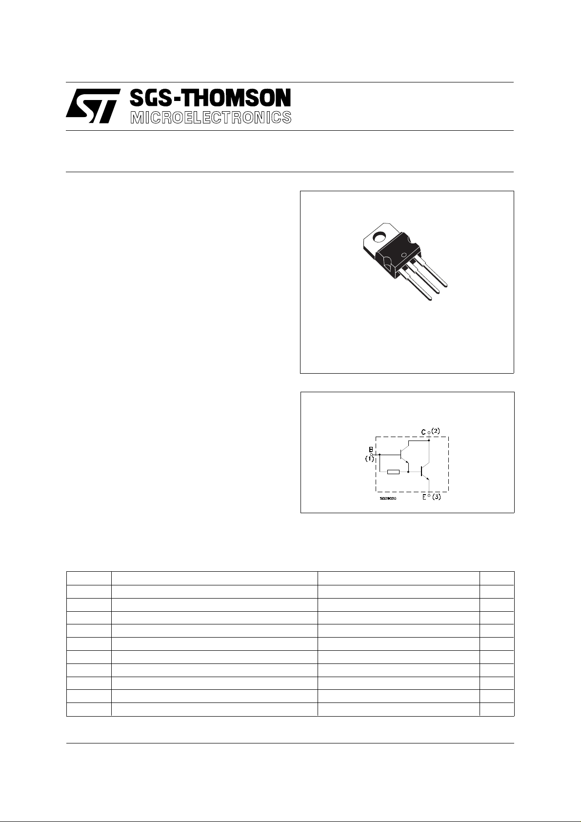
ST901T
NPN POWER DARLINGTON
3
2
1
DESCRIPTION
The ST901T is a high voltage NPN silicon
TO-220
transistor in monolithic special Darlington
configuration mounted in Jedec TO-220 plastic
package, designed for applications such as
electronic ignition for small engines (scooters,
lawnmowers, chainsaws).
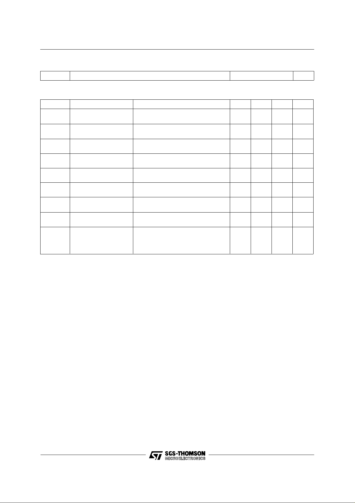
INTERNAL SCHEMATIC DIAGRAM
ABSOL UT E MAXIMU M RATINGS
Symbol Parameter Value Unit
V
V
V
I
I
P
T
Collector- Emitter Voltage (VBE = 0) 500 V
CES
Collector-Emitter Voltage (IB = 0) 350 V
CEO
Emitter-Base Voltage (IC = 0) 5 V
EBO
Collector Current 4 A
I
C
Collector Peak Current 8 A
CM
Base Current 0.5 A
I
B
Base Peak Current 2.5 A
BM
Total Dissipation at Tc ≤ 25 oC30W
tot
Storage Temperature -65 to 175
stg
Max. Operating Junction Temperature 175
T
j
o
C
o
C
June 1997
1/4
ST901T
THERMAL DATA
R
thj-case
Thermal Resistance Junction-case Max 5
o
C/W
ELECTRICAL CHARACTERISTICS (T
= 25 oC unless otherwise specified)
case
Symbol Parameter Test Conditions Min. Typ. Max. Unit
I
CES
I
CEO
I
EBO
V
CEO(sus)
Collector Cut-off
Current (I
= 0)
E
Collector Cut-off
Current (I
= 0)
B
Emitter Cut-off Current
(I
= 0)
C
∗ Collector-Emitter
= 500 V
V
CE
V
= 500 V T
CE
= 350 V
V
CE
V
= 350 V T
CE
= 5 V 10 µA
V
EB
= 125 oC
case
= 125 oC
case
100
0.5
100
0.5
IC = 10 mA L = 10 mH IB = 0 350 V
Sustaining Voltage
V
CE(sat)
∗ Collector-Emitter
IC = 2 A IB = 20 mA 1.3 V
Saturation Voltage
V
∗ Base-Emitter
BE(sat)
IC = 2 A IB = 20 mA 1.8 V
Saturation Voltage
∗ DC Current Gain IC = 2 A VCE =2 V
h
FE
Functional Test V
I
= 4 A VCE =2 V
C
= 24 V V
CC
clamp
= 350 V
1500
500
4A
L = 4 mH
INDUCTIVE LOAD
t
∗ Pulsed: Pulse duration = 300 µs, duty cycle 1.5 %
Storage Time
s
Fall Time
t
f
V
= 12 V V
CC
clamp
L = 4 mH
I
= 2 A IB = 20 mA
C
V
= -3 V
BE
= 250 V
15
1.5
µA
mA
µA
mA
µs
µs
2/4

E
TO-220 MECHANICAL DATA
ST901T
DIM.
MIN. TYP. MAX. MIN. TYP. MAX.
A 4.40 4.60 0.173 0.181
C 1.23 1.32 0.048 0.051
D 2.40 2.72 0.094 0.107
D1 1.27 0.050
E 0.49 0.70 0.019 0.027
F 0.61 0.88 0.024 0.034
F1 1.14 1.70 0.044 0.067
F2 1.14 1.70 0.044 0.067
G 4.95 5.15 0.194 0.203
G1 2.4 2.7 0.094 0.106
H2 10.0 10.40 0.393 0.409
L2 16.4 0.645
L4 13.0 14.0 0.511 0.551
L5 2.65 2.95 0.104 0.116
L6 15.25 15.75 0.600 0.620
L7 6.2 6.6 0.244 0.260
L9 3.5 3.93 0.137 0.154
DIA. 3.75 3.85 0.147 0.151
mm inch
A
C
D
D1
L2
F1
L5
Dia.
G1
F
F2
L9
G
H2
L7
L6
L4
P011C
3/4

ST901T
Information furnished is believed to be accurate and reliable. However, SGS-THOMSON Microelectronics assumes no responsability for the
consequences of use of such information nor for any infringement of patents or other rights of third parties which may results from its use. No
license is granted by implication or ot h erwise under any patent or patent rights of SGS-THOMSON Microelectronics. Specifi cations mentioned
in this publication are subject to change without notice. This publication sup ersedes and replaces all information previously supplied.
SGS-THOMSON Microelectronics products are not authorized for use as critical components in life support devices or systems without express
written approval of SGS-THOMSON Microelectonics.
© 1997 SGS-THOMSON Microelectronics - Printed in Italy - All Rights Reserved
Australia - Brazil - Canada - China - France - Germany - Hong Kong - Italy - Japan - Korea - Malaysia - Malta - Morocco - The Netherlands -
Singapore - Spain - Sweden - Switzerland - Taiwan - Thailand - United Kingdom - U.S.A
SGS-THOMSON Microelectronics GROUP OF COMPANIES
. . .
4/4
 Loading...