

HIGH SPEED FAX MODEM DATAPUMP
.
ITU-T V.17, V.29, V.27ter, V.21 WITH FAX
SUPPORT
.
ITU-T V.23, V.21, BELL103
.
V.17,V.29 (T104), V.27ter SHORT TRAINS
.
V.33 HALF-DUPLEX
.
1800HzOR 1700HzCARRIER
.
SINGLECHIPCOMPLETEDATA PUMP
.
SINGLE5V POWER SUPPLY :
-
TYPICALACTIVE POWER CONSUMPTION:
375mW
-
LOW POWER MODE (typ. 5mW)
.
EXTENDED MODES OF OPERATIONS :
-
FULL IMPLEMENTATION OF THE V.17,
V.33, V.29 AND V.27ter HANDSHAKES
-
AUTODIAL AND AUTOANSWER CAPABILITY
-
PROGRAMMABLETONE DETECTIONAND
FSK V.21 FLAG PATTERN DETECTION
DURING HIGH SPEED RECEPTION
-
PROGRAMMABLE CALL PROGRESS AND
CALL WAITING TONE DETECTORS INCLUDINGDTMF
-
PROGRAMMABLE CLASS DETECTION
CAPABILITY
-
WIDE DYNAMIC RANGE (>48dB)
-
A-LAWVOICEPCM MODE
ST75C520
PRELIMINARY DATA
DESCRIPTION
The SGS-THOMSONMicroelectronicsST75C520
chip is a highly integrated modem engine, which
can operate with all currently used FAX group III
standardsupto14400bps.FullV.21, V.23and Bell
103 full duplex modem standards are implemented.
PQFP64
(Plastic Quad Flat Pack)
ORDER CODE : ST75C520 PQFP
.
VERSATILEINTERFACES :
-
PARALLEL 64 x 8-BIT DUAL PORT RAM
-
SYNCHRONOUS/HDLC PARALLEL DATA
HANDLING
-
HDLC FRAMING SUPPORT
-
V.24 INTERFACE
-
FULL OPERATING STATUS REAL TIME
MONITORING
-
FULL DIAGNOSTIC CAPABILITY
-
DUAL 8-BIT DAC FOR CONSTELLATION
DISPLAY
June 1995
This isadvance informationon a new productnow in developmentor undergoing evaluation. Detailsare subjectto change without notice.
1/45

ST75C520
CONTENTS Page
I PIN DESCRIPTION .................................................... 3
I.1 PIN CONNECTIONS. . . . . . . . . . . ......................................... 3
I.2 HOSTINTERFACE..................................................... 3
I.3 ANALOGINTERFACE . . . . . . . . .......................................... 4
I.4 V.24INTERFACE. . . ................................................... 4
I.5 MISCELLANOUS . . . ................................................... 4
I.6 BOUNDARYSCANINTERFACE . . . . . . . . . . . . . ............................. 4
I.7 POWER SUPPLY. . . . . . .. . ............................................. 5
II BLOCK DIAGRAMS.................................................... 5
III ELECTRICALSPECIFICATIONS ......................................... 6
III.1 MAXIMUMRATINGS . . . . . . . . . .......................................... 6
III.2 DC CHARACTERISTICS . . . . . . . . . ....................................... 6
III.3 AC CHARACTERISTICS . . . . . . . . . ....................................... 8
IV FUNCTIONAL DESCRIPTION............................................ 10
IV.1 SYSTEMARCHITECTURE . ............................................. 10
IV.2 OPERATION. . . . ...................................................... 10
IV.3 MODEMINTERFACE. . . . . . . . . . . . . . . . . . . . . .. . . . . . .. . .................... 11
V. USER INTERFACE..................................................... 11
V.1 DUALPORT RAM DESCRIPTION. . ....................................... 11
V.2 COMMANDSET. . . .. . . . . . . . . . . . ....................................... 14
V.3 COMMANDSET SHORT FORM . . . . . . . . . . . . . ............................. 16
V.4 STATUS- REPORTS. . . . . . ............................................. 17
V.5 DATA EXCHANGES. . . . . . . .. . .......................................... 17
VI COMMANDSETDESCRIPTION .......................................... 18
VII STATUSDESCRIPTION ................................................ 27
VII.1 COMMANDACKNOWLEDGEAND REPORT. . . ............................. 27
VII.2 MODEMSTATUS. . . ................................................... 28
VIII TONEDETECTORS.................................................... 34
VIII.1 OVERVIEW. .......................................................... 34
VIII.2 DESCRIPTION . ....................................................... 34
VIII.3 EXAMPLE. . . . . . . . . .. . .. . ............................................. 38
IX BUFFEROPERATIONS................................................. 38
IX.1 INTRODUCTION. . . . . . . . . . .. . . . . . . . .. . .. . . ............................. 38
IX.2 RECEIVEOPERATIONSOVERVIEW. . . . . . . . . .. . .......................... 39
IX.3 TRANSMIT OPERATIONSOVERVIEW. .................................... 39
IX.4 BUFFERSTATUS AND FORMAT DESCRIPTION . . . . . . . . . . . . . . . . . . . . . ....... 40
IX.5 RECEIVEBUFFER. . . . . . . . . . . . ......................................... 40
IX.6 DATA BUFFERMANAGEMENT.. . . . . . .................................... 40
X DEFAULT CALL PROGRESS TONEDETECTORS........................... 42
XI DEFAULT ANSWER TONE DETECTORS .................................. 42
XII ELECTRICALSCHEMATICS............................................. 42
XIII PCB DESIGN GUIDELINES.............................................. 43
2/45

I - PIN DESCRIPTION
I.1 - Pin Connections
ST75C520
SA0
SA1
SA2
SA3
SA4
SA5
SA6
GND
V
DD
SD0
SD1
SD2
SD3
SD4
SD5
SD6
17
18
19
20
21
22
23
24
25
26
27
28
29
30
31
32
TXD
RXD
CLKCDCTS
38 39 40 41 42 43 44 45 46 47 4833 34 35 36 37
RTS
RING
DD
GND
EYEX
EYEY
TEST2
EBS
TXA2
V
TEST1
TXA1
12345678910111213141516
64
63
62
61
60
59
58
57
56
55
54
53
52
51
50
49
AGNDT
V
CM
AV
DD
RXA2
RXA1
AGNDR
V
REFP
V
REFN
EXTAL
XTAL
CLKOUT
HALT
RESET
SCOUT
BOS
EOS
SD7
SDS (SRD)
SR/W (SWR)
SCS
SINTR
SDTACK
GND
INT/MOT
DD
V
SCIN
MCI
SCCLK
RDYS
MC2
MC1
MC0
I.2 - Host Interface
The exchangeswith the control processor proceed through a 64 BytesDUALport RAM shared between
the ST75C520 and the Host. The signalsassociatedwiththis interfaceare:
Pin Name Type Description
SD0..SD7 I/O System Data Bus. 8-bit data bus used forasynchronous exchanges between the ST75C520
SA0..SA6 I System Address Bus. 7-bit address bus for dual port RAM.
SDS (SRD) I System Data Strobe. Active low. Synchronizes allthe exchanges. In Motorolamode initiates
SR/W (SWR) I System Read/Write. In Motorola mode defines the type of exchange read/write. In Intel
SCS I System Chip Select. Active low.
SDTACK OD System Bus Data Acknowledge. Active low. Open drain.
SINTR OD System Interrupt Request.Active low. This signal is asserted by the ST75C520 and
RESET I Reset. Active low.
RING I Ring Detect Signal. Active low.
INT/MOT I Select Intel/Motorola Interface.
and the Host through the dualport RAM. High impedance when exchanges are not active.
the exchange, activelow. InIntelmode initiates a read exchange, activelow.
mode initiates awrite exchange, active low.
negated by thehost. Open drain.
75C52001.EPS
3/45
ST75C520
I.3 - AnalogInterface
Pin
Name
TXA1 O Transmit Analog Output 1
TXA2 O Transmit Analog Output2.OutputsTXA1andTXA2 provideanalogsignalswithmaximum peaktopeak
RXA1 I Receive AnalogInput 1
RXA2 I Receive AnalogInput 2. The analog differential input peak to peak signal must beless than 2 x V
V
V
V
I.4 - V.24 Interface
Pin Name Type Description
RTS I Request to Send. Active low.
CLK O Data Bit Clock. Fallingedge coïncides with DATA change.
CTS O Clear to Send. Active low.
RxD O Receive Data
TxD I Transmit Data sampled withrising edge of CLK
CD O Carrier Detect. Active low.
Type Description
amplitude 2xV
V
REF=VREFP-VREFN
, and must befollowedby an external continous-time twopole smoothingfilter (where
REF
).
must be preceded by an external continous-time single pole anti-aliasing filter. This filter must be as
close as possibleto the RXA1 and RXA2 Pins (where V
CM
REFN
REFP
I/O Analog CommonVoltage (nominal +2.5V). This input must be decoupled with respect to AGND.
I Analog Negative Reference (nominal VCM- 1.25V). This input must be decoupled with respect to VCM.
I Analog Positive Reference (nominalVCM+1.25V). This input must be decoupled with respect to VCM.
REF=VREFP-VREFN
REF
).
.It
I.5 - Miscellaneous
Pin Name Type Description
XTAL O Internal Oscillator Output. Left open if not used.
EXTAL I InternalOscillator Input, or External Clock
EYEX O Constellation X analog coordinate
EYEY O Constellation Y analog coordinate
TEST1 To be left open
TEST2 To be left open
Note : The nominal external clock frequency of the ST75C520 is 29.4912MHz with a precision better than ± 5.10
-5
I.6 - BoundaryScanInterface
Aset of 13 signals arededicated for Testingthe ST75C520 Component. Thesesignals can be used in a
developmentphase,associatedwith the SGS-THOMSONST18932 BoundaryScanDevelopment Tools,
to Debug the applicationHardware and Software.If not used all input signals must be grounded and all
output signals left open.
Pin Name Type Description
SCIN I Scan Data Input
SCCLK I Scan Clock
SCOUT O Scan Data Output
BOS I Begin of Scan Control
EOS I End of Scan
MC0..MC2 I Mode Control
HALT I Stop ST75C520 Execution
MCI O Multicycle Instruction
RDYS O Ready to Scan Flag
EBS I Enable Boundary Scan. Active low (mustbe set low in normal mode).
CLKOUT O InternalST75C520 Clock (XTAL frequency divided by 2)
4/45

ST75C520
I.7 - PowerSupply
Symbol Parameter
V
DD
GND Digital Ground (Pin8, 24, 40). To be connected to AGNDT and AGNDR (see below).
AV
DD
AGNDT Analog Transmit Ground (Pin 64). To be connected to GND (see below).
AGNDR Analog Receive Ground (Pin59). To be connected to GND (see below).
AGNDTand AGNDRmust be connectedtogetherascloseas possibleto the chip.
GNDand AGNDRboardplansshould be separated,then connectedtogether as closeas possible to the
chip, at a single point. Similarly V
singlepoint.
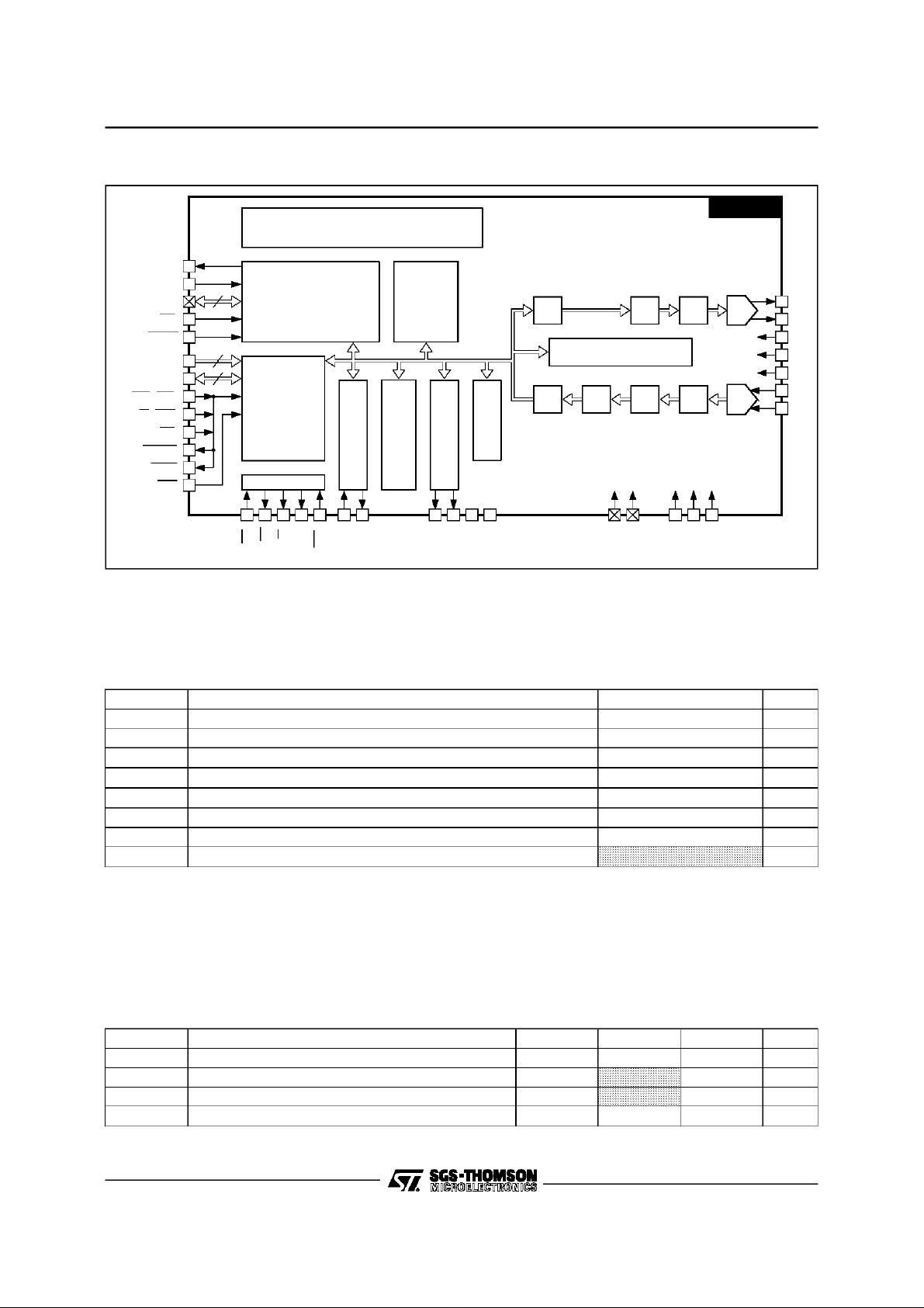
II - BLOCK DIAGRAMS
II.1 - Functional Block Diagram
Digital +5V (Pin 9, 25, 41). To be connected to AVDD(see below).
Analog +5V(Pin 62). To be connected to VDD(see below).
and AVDDmust ne connected as close as possible to the chip, at a
DD
RXD
TXD
CLK
15 16 14
ST75C520
HDLC
TX
MUX
V.17, V.29, V.27
FAX TRANSMITTER
TX
ANALOG
1
TXA2
2
TXA1
SD [0..7]
(26 to 33)
SINTR
DUAL RAM
INTERFACE
HDLC
RX
HANDSHAKE AND
38
STATUS REPORT
RTS
RING
DETECTOR
V.24
INTERFACE
13 1112 10
CD
CTS
RING
V.17, V.29, V.27
FAX RECEIVER
TONE
DETECTOR
V.21 FLAG
DETECTOR
DPLL
RX
ANALOG
60
RXA1
RXA2
61
75C52002.EPS
5/45
ST75C520
II.2 - HardwareBlockDiagram
XTAL
55
EXTAL
56
BOUNDARYSCAN
(42 to51 - 53-54)
EBS
RESET
SA [0..6]
(17 to 23)
SD [0..7]
(26 to 33)
SDS (SDR)
SR/W (SWR)
SCS
SDTACK
SINTR
12
3
52
7
8
34
35
36
37
38
39INT/MOT
11 12 13 14 10
DSPCORE
DUAL
PORT
RAM
64 x8
V.24INTERFACE
CD
CTS
RTS
ST18932
CLK
PROGRAM ROM 8Kx 32
RAM
2K x 16
S
S
CROM
S
8K x16
I
O
16 15 7 6 5 4
TXD
RXD
RING
E
Y
E
EYEX
EYEY
P
A
G
E
TEST1
TEST2
FIFO
8x16
FIFO
8x16
IIR FIR
DPLL AND CONTROL
FIR
8-24
40
IIR FIR
DD
DV
DGND
9-25
41
59 62 64
DD
AV
AGNDR
ST75C520
AGNDT
TXA2
1
TXA1
2
58
V
REFP
63
V
CM
57
V
REFN
60
RXA1
61
RXA2
75C52003.EPS
III - ELECTRICALSPECIFICATIONS
Unless otherwisenoted,electrical characteristicsare specifiedovertheoperatingrange.Typicalvalue are
given for V
= +5V andt
DD
amb
=25°C.
III.1 - MaximumRatings (referencedto GND)
Symbol Parameter Value Unit
V
DD
V
I,VIN
I
I,IIN
I
O
I
OUT
T
oper
T
stg
P
tot
Stresses above those hereby listed maycause damage to thedevice. The ratingsarestress related onlyand functional operation ofthe device
at conditions beyond those indicated inthe operational sections of the specificationsis not implied. Exposure to maximumrating conditions for
extended periods may affect device reliability. Standard MOS circuits handling procedure should be used to avoid possible damage to the
device.
DC Supply Voltage -0.3 to 7.0 V
Digital or Analog Input Voltage -0.3 to(VDD+ 0.3) V
Digital or Analog Input Current ±
Digital Output Current ±
Analog Output Current ±
1
20
10
mA
mA
mA
Operating Temperature 0, + 70 °C
Storage Temperature (plastic) - 40, + 125 °C
Maximum Power Dissipation 1000 mW
III.2 - DC Characteristics
V
= 5.0V ± 5%, GND=0V,T
DD
=0 to 70°C(unlessotherwisespecified).
amb
III.2.1 - PowerSupply and Common Mode Voltage
Symbol Parameter Min. Typ. Max. Unit
V
I
DD
I
DD-lp
V
DD
CM
SupplyVoltage 4.75 5 5.25 V
SupplyCurrent (internal oscillator) 75 100 mA
SupplyCurrent in Low Power Mode 1 mA
Common Mode Voltage VDD/2 -5% VDD/2 VDD/2 + 5% V
6/45
ST75C520
III.2.2 - DigitalInterface
Alldigital pins except XTALPins.
Symbol Parameter Min. Typ. Max. Unit
V
IL
V
IH
I
I
V
OH
V
OL
I
OZ
C
IN
Crystaloscillatorinterface(XTAL, EXTAL).
Symbol Parameter Min. Typ. Max. Unit
V
IL
V
IH
I
L
I
H
III.2.3 - AnalogInterface
Symbol Parameter Min. Typ. Max. Unit
V
REF
V
CMOin
V
DIFin
V
CMOout
V
DIFout
VOFFOut Differential Output DC Offset (TXA1 - TXA2) -100 100 mV
Rin Input Resistance RXAx 100
Rout OutputResistance TXAx 20 Ω
RL Load Resistance TXAx 10
CL Load Capacitance TXAx 50 pF
Low Level InputVoltage -0.3 0.8 V
High Level InputVoltage 2.2 V
Input Current VI=VDDor VI= GND -10 0 +10
High Level OutputVoltage (I
Low Level Output Voltage (I
= 2mA) 2.4 V
load
= 2mA) 0.4 V
load
Three State Input Leakage Current (GND < VO<VDD) -50 0 50 µ
Input Capacitance 5 pF
Low Level InputVoltage 1.5 V
High Level InputVoltage 3.5 V
Low Level InputCurrent GND < VI<V
High Level InputCurrent VIHmin< VI<V
Differential Reference VoltageInput = V
Input Common Mode Offset,v = (RXA1+RXA2)/2 - V
ILmax
DD
REFP-VREFN
CM
Differential Input Voltage RXA1 - RXA2 2 x V
Output Common Mode Voltage Offset = (TXA1+TXA2)/2 - V
CM
Differential Output Voltage TXA1 - TXA2 2 x V
-15 µ
15 µ
2.40 2.50 2.60 V
-300 300 mV
REF
-200 200 mV
REF
V
V
kΩ
kΩ
µA
A
A
A
PP
PP
7/45

ST75C520
III.3 - AC ElectricalCharacteristics
III.3.1 - Dual PortRAM Host Timing
NSCS
SA[0..6]
SR/NW
NSDS
Motorola modeIntel mode
SD[0..7]
NSDTACK
WRITE-CYCLE TIMING
Valid Address
174
8
3 5 10 5
Valid Data
IN
26 26
11
READ-CYCLE TIMING
Valid Address
194
12
Valid Data
OUT
NSINTR
SR/NW (= NWRITE)
NSDS (= NREAD)
Number Description Min. Typ. Max. Unit
1 Address and Control Set-up Time 5 ns
2 SDTACK Acknowledge 20 ns
3 Data Set-up Time 10 ns
4 Address and Control Hold Time 0 ns
5 Data HoldTime 5 ns
6 SDTACK Hold Time 0 ns
7 Write Enable Low State 45 ns
8 Access Inhibition High State (see Note) 70 ns
9 Read Enable Low State 45 ns
10 Read Data Access 35 ns
11 SINTR Clear Delay 50 ns
12 Data Valid to Tristate 15 ns
Note : A minimum delay of70nsis required only fromthe rizing edge ofNWRITE tothefallingedge ofthe nextselected NREAD orNWRITE.
75C52004.EPS
8/45

III.3.2 - SerialV.24 Interface Timing
CLK
ST75C520
12
TXD
Valid Data In
3
RXD
Valid Data Out
4
Number Description Min. Typ. Max. Unit
1 TXD to CLK Set-up Time 30 ns
2 TXD to CLK Hold Time 10 ns
3 RXD Validto CLK Delay Time 100 ns
4 RXD Validto CLK HoldTime 0 ns
75C52005.EPS
9/45

ST75C520
IV - FUNCTIONALDESCRIPTION
IV.1 - SystemArchitecture
The chip allows the design of a complete FAX
data-pumpwithout any externalcomponent.Aversatiledual port RAM allows an easy interfacewith
mostmicro-controllers.
IV.2 - Operation
IV.2.1- Modes
Themodemimplementationisfullycompatiblewith
FAX modulation recommendations. The modulation can be either TrellisCoded Modulation(TCM)
as in V.17 14400, 12000, 9600, 7200bps rates,
Quadrature Amplitude Modulation (QAM) as in
V.29 9600, 7200, 4800 and V.27ter 4800 and
2400bps. Other modes of operation include tone
and DTMF detection or generation, or speech
mode.
IV.2.2- TransmitterDescription
The signalpulses are shaped in a dedicatedfilter
further combined with a compromise transmit
equalizersuitedfortransmissionoverstronglydistortedlines. 3 different compromise equalizersare
availableand can be selectedby software.
IV.2.3- ReceiverDescription
The receiver section handlescomplex signals and
usesa fractionally spaced complex equalizer. It is
able to copewithdistantmodemtiming drifts up to
-4
asspecifiedinthe ITU-T recommendations.It
10
alsocompensateforfrequencydriftup to 10Hzand
for phase jitter at multiple and simultaneous frequencies.
IV.2.4- ToneGeneratorDescription
Fourtonescanbesimultaneouslygeneratedbythe
ST75C520. The tones are determined by their
frequenciesandbytheoutputamplitudelevel.Aset
of specific commandsare also available for DTMF
generation(using two of the four generatorsavailable).
IV.2.5- ToneDetectorDescription
Sixteen tones can be simultaneouslydetected by
the ST75C520.Eachofthe tonesto bedetectedis
defined by the coefficientsof a 4th order programmableIIR. Detectionthresholds are also programmablefrom-45dBmupto-10dBm.DTMFdetection
isalsoavailableand isperformedbya specificfilter
section (that requires no programming).
IV.2.6- DTMF Detector Description
A DTMF Detector is included in the ST75C520, it
allowsdetectionofvalidDTMFDigits.AvalidDTMF
Digit is defined as a dual Tone with a total power
higher than -35dBm,a durationhigher than 40ms
and a differentialamplitudewithin 8dB(negativeor
positive).
IV.2.7- VoiceMode
The ST75C520 voice mode allows the implementation of enhanced telephone functions like answering machines. The incoming samples
(9600Hz), received from the line are PCM A-law
coded and writen into the dual port RAM. The
outpoing samples are decompressed using the
same A-law and output to the telephoneline.
The voice mode is entered using a CONF command, it canbe either transmit voice from thedual
RAM Tx bufferto the telephoneline,receivevoice
from the telephone line to the dual RAM buffer,or
both of these functions simultaneously. The format
of thesignal isA-law codedwithout complementation of the even bits. The buffer mechanism, between thehostmicro-controler andtheST75C520,
is identicaltothemechanismusedforparalleldata
exchanges except that it starts immediately after
CONF command, the size of the transmit and
received buffer,are and must be 8 bytes, there is
no needfor aXMITcommand, andifan overrunor
underrunconditionoccursno error willbe reported
to thehost processor.
IV.2.8- Analog Loop Back Test Mode
In any transmission standard and serial data format, the ST75C520can be configured for analog
loop backtest.
IV.2.9- Low Power Mode
Sleepstatecan beattainedby a SLEEPcommand.
Activating the reset signal will wake up the datapump. Whenin sleep mode, the dual port RAM is
unavailableand theclocksare disabled.
Whenenteringthe lowpowermode,theST75C520
stops its oscillator, all the peripherals of the DSP
core are stopped in order to reduce the power
consumption.Thedual RAM is made inacessible.
The ST75C520 can be awakened by a hardware
reset.
There is a maximum time of 20ms to restart the
oscillator after waking up and an additional 5ms
after the interrupt to be able to accept any command coming from the host.
10/45

ST75C520
IV.2.10- Reset
After a hardware reset, or an INIT command, the
ST75C520 clears all its internal memories, clears
thewhole dual RAMand startsto initialize thedelta
sigma analog converters.As soon as theseinitializations are completed, the ST75C520 clears the
dual RAM address 0 (COMSYS), generates an
interrupt IT6 (command acknoledge) and is programmed to send and receive tones, the bit clock
and the sample clock areprogrammedto 9600Hz.
The total duration of the reset sequence is about
5ms. After that time the ST75C520 is ready to
executecommands sentby the host micro-controller.Thedurationoftheresetsignalshouldbegreater
than700ns.
IV.3 - Modem Interface
IV.3.1- AnalogInterface
Themodemdesigner must provideaproperhybrid
interface to the ST75C520. An example of hybrid
design is given in paragraphs XII and XIII. The
inputs and outputs of the MAFE are differential,
achieving thus a better noise immunity. The D/A
converter output amplifier includes a single pole
low-passfilter, its cut-off frequencyis :
- 3dB # 19200Hz.
F
c
Continuous-timefiltering of the analog differential
output is necessaryusingan off-chip amplifierand
a fewexternalpassivecomponents.
IV.3.2- Host Interface
The host interface is seen by the micro as a 64x8
RAM, with additional registers accessiblethrough
an 8-bit address space.Aselection Pin(INT/MOT)
allowstoconfigurethehostbusfor eitherINTELor
MOTOROLAtypecontrolsignals.
V.1.1- Mapping
V.1.1.1- CommandArea
The command area is located from $00 to $04.
Address $00 holds the commandbyte COMSYS,
and the next four locations hold the parameters
COMPAR[0..3]. The command parameters must
be entered before the command word is issued.
Once the command has been entered, the command byte is reset and an acknowledge report is
issued. A new command should not be issued
beforetheacknowledgecounterCOMACKisincremented.
V.1.1.2- ReportArea
The report area is located from address $05 to
address $07.Location$05holdsthe acknowledge
counter COMACK. Each time a command is acknowledged, the report bytes COMREP[0..1] (if
any) are written by the ST75C520 into locations
$06 and $07, and the content of COMACK is
incremented.This counterallowsthe ST75C520to
accurately monitor the command processing.
V.1.1.3- StatusArea
Thestatusareaislocatedfromaddress$08to$0A.
The error status word SYSERR is located at address$08. Thiserror statusword isupdated each
time anerrorconditionoccurs.Anoptionalinterruption IT0 may additionally be triggered in the case
of an error condition. Locations$09 and $0A hold
the generalstatusbytes STATUS[0..1]. The meaning of the bitsdepends on the mode of operation,
and is described in Chapter VII. The third byte at
address $0B holds the Quality Monitor byte
STAQUA.
V - USER INTERFACE
V.1 - Dual PortRam Description
ThedualportRAMisthestandardinterfacebetween
the controller and the ST75C520, for either commandsordata.Thismemoryis addressedthrougha
7-bitaddressbus.Thelocationsfrom$00 to$3Fare
RAMlocations,while locationsfrom $40 to$50 are
controlregistersdedicatedtotheinterrupt handling.
Severalfunctionalareasaredefinedinthedualport
RAM, namely :
- thecommand area,
- thereport area,
- thestatusarea,
- thedata bufferarea.
V.1.1.4- Optional StatusArea
The user can program (through the DOSR command) the three locations STAOPT[0..2] of the
OptionalStatusArea ($0C to $0E) for the real time
monitoring of threearbitrarymemorylocations.
V.1.1.5- DataBuffer Area
The data area is made of four 8-bytebuffers. Two
are dedicated to transmission and the two others
to reception.Eachof thefour buffers is attached to
a status byte. the meaning of the status byte depends on the selected format of transmission.
Within each buffer, D0 represents the first bit in
time.
11/45

ST75C520
V.1.2- Interruptions
The ST75C520 can generate 5 interrupts for the
controller.The interrupthandlingis made withaset
of registers located from $40 to $50.
The interruptions generated by the ST75C520
come from several different sources. Once the
ST75C520 raises an interrupt, a signal is sent to
the controller. The controller has then to process
the interrupt and clear it.The interrupt source can
be examined in the Interrupt Source Register
ITSRCR located at $50. According to this status
byte,theinterruptsourcecanbedetermined.Then,
writing azero at oneof thememorylocation$40to
$46 (Reset Interrupt Registers ITREST[0..6]) will
reset the corresponding interrupt (and thus acknowledgeit). These sources of interruptions can
be masked globally or individually using the Interrupt Mask Register ITMASKlocatedat $4F.
The interrupt sources are :
- IT0 : Error/Warning
This signifies that an error has occurredand the
error code is available in the error status byte
SYSERR.This byte can be selectivelycleared by
the CSE command.
- IT2 : Tx Buffer
Each time the ST75C520 frees a buffer, this
interruptis generated.
- IT3 : Rx Buffer
Each time the ST75C520 has filled a buffer, this
interrupt is generated.
- IT4 : StatusByte
This signifies that the status byte has changed
and must be checked by the controller.
- IT6 : Command Acknowledge
ThissignifiesthattheST75C520hasreadthelast
command entered by the host, incrementedthe
command counter COMACK, and is ready for a
new command.
ITSRCR X D6 X D4 D3 D2 X D0
D0 =1 IT0 Pending
D2 =1 IT2 Pending
Dn =1 ITn Pending
ITMASK D7 D6 X D4 D3 D2 X D0
D7 andD0 = 1 IT0 EnableD
D7 andD2 = 1 IT2 EnableD
...................... .....................
D7 andD6 = 1 IT6 EnableD
12/45

ST75C520
V.1.3- Host InterfaceSummary
Address (hex) Description Size (Byte) Mnemonic
COMMAND AREA
$00 Command 1 COMSYS
$01-$04 Command Parameters 4 COMPAR[0..3]
REPORT AREA
$05 Acknowledge Counter 1 COMACK
$06-$07 Report 2 COMREP[0..1]
STATUS AREA
$08 Error Status 1 SYSERR
$09-$0A General Status 2 STATUS[0..1]
$0B Quality Monitor 1 STAQUA
$0C-$0E Optional Report 3 STAOPT[0..2]
DATA AREA
$1C Data Rx Buffer0 Status 1 DTRBS0
$1D-$24 Data Rx Buffer0 8 DTRBF0[0..7]
$25 Data Rx Buffer 1 Status 1 DTRBS1
$26-$2D Data Rx Buffer1 8 DTRBF1[0..7]
$2E Data Tx Buffer 0 Status 1 DTTBS0
$2F-$36 Data Tx Buffer0 8 DTTBF0[0..7]
$37 Data Tx Buffer 1 Status 1 DTTBS1
$38-$3F Data Tx Buffer1 8 DTTBF1[0..7]
INTERRUPT AREA
$40-$46 Reset InterruptReg. 7 ITREST[0..6]
$4F Interrupt Mask Reg. 1 ITMASK
$50 Interrupt Source Reg. 1 ITSRCR
13/45

ST75C520
V.2 - Command Set
The Command Set has the following attractive
features :
- userfriendlywitheasyto remembermnemonics,
- possibilityof straightforwardexpansionwithnew
commands to suit specific customer requirements,
- easyupgradeofexisting software usingprevious
modem based SGS-THOMSONproducts.
The command set has been designed to provide
the necessaryfunctionalcontrolon theST75C520.
Eachcommandisclassified accordingtoitssyntax
and the presence/absenceof parameters. In the
case of a parametriccommand,parameters must
first be written into the dual port RAM before the
commandisissued. Acknowledgeand errorreport
isissued for eachcommand entered.
V.2.1- Command SetSummary
V.2.1.1- OperationalControl Commands
INIT Initialize. Initialize the modem engine.
Setallparameterstotheirdefault values
and wait for commands of the control
processor. Non parametriccommand.
IDT Identify. Returntheproductidentification
code.Non parametric command.
SLEEP Turntolow power mode, the ST75C520
entersthelowpowermode and stopsits
crystal oscillator to reduce power
consumption.In this mode allthe clocks
are stopped and the du al RAM is
unreachable.
HSHK Handshake. B egins the handshake
sequence. The modem engine
generates all the sequences defined in
the ITU-T recommendations. A status
reportindicatesto thecontrol processor
the state of the handshake. This
commandonly applies to modes where
a handshake sequence is defined. A
CONFcommandmusthavebeenissued
priortotheuseofHSHK. Nonparametric
command.
STOP FAX Sto p. Stop FAX Half-duplex
transmitter. Nonparametriccommand.
SYNC FAX Synchronize. Start/Stop of FAX
Half-duplex receiver. Par ametric
command.
CSE Clear StatusError. Selectivelyclearsthe
Error status byte SYSERR. Parametric
command.
SETGN Set Gain. This command sets theglobal
gain factor,whichisused for thetransmit
samples.Parametriccommand.
V.2.1.2- Data CommunicationCommands
XMIT Transmit Data. Start/stop the
transmission of data in parallel mode.
After a XMIT command, the ST75C520
sends the data containedin its dualport
RAM.
SERIAL Select Serial or Parallel Mode. This
command selects the data source, i.e.
either parallel or serial. The parallel
mode uses a part of the dual port RAM
as a doublebuffer.Theserialmodeuses
the serial synchronous I/O. Parametric
command.
FORM SelectstheTransmissionFormat(onlyin
parallel mode). This command
configures the data interface for both
receiverandtransmitteraccordingtothe
selected data format. Parametric
command (HDLC or synchronous). In
serial mode, format is always
synchronous.
V.2.1.3- MemoryHandling Commands
MW Memory Write.This commandisusedto
write an arbitrary 16-bit value into the
writa ble me mo r y locatio n curren t ly
specified by a parameter. Parametric
command.
MR MemoryRead.Thiscommandallowsthe
controller to read any of the ERAM or
CROM (ST75C520 memory spaces)
loca tion without int errupting t he
processor. Parametriccommand.
CR Complex Read. This command allows
the controller to read at the same time
the real and imaginarypartofacomplex
value stored in a double ERAM or
CROM location. This feature is very
interesting for eye pattern software
control and for equalization monitoring.
This command insures that the real and
imaginary parts are sampled in the
memory at the same time (integrity).
Parametric command.
14/45

ST75C520
V.2.1.4- Configuration Control Commands
CONF Configure.Thiscommandconfiguresthe
modemenginefordatatransmissionand
handshakeprocedures(ifany) in any of
the supported modes. Thetransmission
parametersaresetto theirdefaultvalues
and can be modified with the MODC
command.Parametriccommand.
MODC Modify Configuration. This command
allows modification of some of the
parameters which have been set up by
theCONFcommand.It canalsobeused
to alter the mode of operations (short
train).Parametriccommand.
DOSR Define Optional Status Report. This
commandallows the modificationof the
optional status report located in the
status area of the dual port RAM. One
canthusselectaparticularparameterto
be mo nitor ed during al l modes of
operation.Parametriccommand.
DSIT Define Status Interrupt. This command
allows the programming of the status
word bitthatwillgeneratean Interruptto
the controller.Parametriccommand.
DEFT Define Tone. Programs the tone
generator(s)forarbitrarytone synthesis.
Parametriccommand.
TGEN Tone Generator Control. Enables or
disables the tone generator(s).
Parametriccommand.
IV.2.1.6-Tone Detection Commands
TDRC Read Tone Detector Coefficient. Read
one To ne Detector Coefficient.
Parametriccommand.
TDWC Write Tone Detector Coefficient. Write
one To ne Detector Coefficient.
Parametriccommand.
TDRW Read Tone Detector Wiring. Read one
Tone Detector Wiring connection.
Parametriccommand.
TDWW Write Tone Detector Wiring. Write one
Tone Detector Wiring connection.
Parametriccommand.
TDZ Clear ToneDetector Cell. Clear internal
variables of a Tone Detect or Cell.
Parametriccommand.
V.2.1.5- Tone GenerationCommands
TONE Select Tone. Programs the tone
generator(s) for the desired default
tone(s). Additional mnemonics provide
quick programming of DTMF tones or
other currently used tones. Parametric
command.
V.2.1.7- MiscellaneousCommands
CALL Call a Subroutine.Call asubroutinewith
one Parameter.Parametriccommand.
JSR Call a Low Level Subroutine. Call an
internal subroutine with one parameter.
Parametriccommand.
15/45

ST75C520
V.3 - Command Set Short Form
CCI Command
Mnemonic Value Description
XMIT 0x01 Transmit Data
SETGN 0x02 Set Transmit Gain
SLEEP 0x03 Power Down the ST75C520
HSHK 0x04 Start Handshake
INIT 0x06 Initialize (Software Master RESET)
SERIAL 0x07 Enable/disable Data Serial Mode
CSE 0x08 Clear Error Status Word
FORM 0x09 Define Parallel Data Format
DOSR 0x0A Define Optional Status Report
TONE 0x0C Generate PredefinedTones
TGEN 0x0D Enable Tone Generator
DEFT 0x0E Define Arbitrary Tone
MR 0x10 Memory Read
CR 0x11 Complex Read
MW 0x12 Memory Write
DSIT 0x13 Define Status Interrupt
IDT 0x14 Return ProductIdentification Code
JSR 0x18 Call a Low Level Subroutine
CALL 0x19 Call a Subroutine
TDRC 0x1A Tone Detector Read Coefficient
TDRW 0x1B Tone Detector ReadWiring
TDWC 0x1C Tone Detector Write Coefficient
TDWW 0x1D Tone Detector Write Wiring
TDZ 0x1E Tone Detector ClearCell
CONF 0x20 Configure
MODC 0x21 Modify Default Configuration
STOP 0x25 FAX Stop Transmitter
SYNC 0x26 FAX Synchronize Receiver
16/45

ST75C520
V.4 - Status - Reports
V.4.1- Status
The ST75C520 has a dedicated status reporting
area located in its dual port RAM. This allow a
continuousmonitoringof the status variables without interruptingthe ST75C520.
The first statusbyte gives the error status. Issuing
of an error status can also be flagged by a maskable interruptfor the controller. Thesignification of
the error codes are given in Chapter VII.
The secondand thirdstatusbytesgivethegeneral
status of the modem. These status include for
example the ITU-T circuit status and other items
describedinappendix. Thesetwo status can generate, when a change occurs, an interrupt to the
controller ; each bit of the two byte word can be
maskedindependently.
The forth byte gives in real time a measure of the
receptionquality.Thisinformationmay be used by
the controller to monitorthe qualityof the received
bits.
Three other locations are dedicated for custom
status reporting. The controller can program the
ST75C520for a real time monitoring of any of its
internalRAM location.High byteor low byte of any
word can thus be monitored.
V.4.2- Reports
The ST75C520 features an acknowledge and report facility. The acknowledge of a command is
monitored by a counter COMACK located in the
dual portRAM. Each time a commandisreadfrom
the command area, the ST75C520will increment
this counter. For instance, when a MR (Memory
Read) command is issued, the data is first written
in the report area, and the counter is incremented
afterwards. This way of processing insures data
integrity and gives additional synchronization between the controller and the data pump.
V.5 - Data Exchanges
The ST75C520 accepts many kinds of data exchange : the default mode uses the synchronous
serialexchange.OthermodesincludeHDLCframing support and synchronousparallel exchanges.
Detaileddescriptionof the DataBufferExchanges
modesis available in the paragraph IX.
V.5.1- Synchronous Parallel Mode
The data exchanges are made through the dual
port RAM andarebyte synchronousoriented.The
double buffer facilities of the ST75C520 allow an
efficientbufferingof the data.
V.5.1.1- Transmit
Thecontrollermustfirstfillatleastthefi r s tbufferof data
(TxBuffer0) withthebitsto be transmi t ted.In orderto
performthisoperation,thecontrollermustfirst check
the Tx Buffer0 statusword DTTBS0.If this bufferis
empty, the controllerfills thedatabufferlocations(up
to 64 bits ) ,andthenwritesinDTT BS0thenumberof
bytescontainedin thebuffer. The controllercan then
either proc eed with the second buffer or initiate the
transmi ssio nwi t haXMI Tcommand.
The ST75C520 copies the contents of the data
buffer and then clears the buffer status word in
order tomakeitagainavailable,thengeneratesan
IT2 interrupt. The numberof bytesspecifiedbythe
status word is then queued for transmission. The
process goeson withthe two buffers untilan XMIT
commandstops the transmission. After the finishing XMITcommand has beenissued,the last buffers areemptiedby theST75C520.
Errorsoccurwhenbothbuffersareemptywhilethe
transmit bit queue is also empty.Erroris signalled
with an IT0 interruptionto the controller.
V.5.1.2- Receive
The controllershouldtakecareof releasingthe Rx
buffers before the Data Carrier Detect goes true.
This ismadebywriting zeroin the RxBufferStatus
0 and 1. The ST75C520 then fills the first buffer,
and oncefilledsetsthe statuswordwiththe number
of bytesreceived and thengeneratesan IT3 interrupt. It then takes control of the secondbufferand
operatesthe same way. The controllermustcheck
the statusof thebuffersandempty them. Oncethe
data read, the controller must release the used
buffer and wait for thenext buffer to be filled.
Error occurs when both buffers are declared full,
and incomingbits continue to arrive from the line.
Error is signaledby an IT0interrupt.
V.5.2- HDLC Parallel Mode
This mode implementspartof the High Level Data
Link Control formats and procedures. It is well
suited for error correcting protocols like ECM or
FAXT4/T30recommendations.Itsupportstheflagging generation,16-bitFrameCheckSequence,as
well as the Zero insertion/deletionmechanism.
V.5.3- Serial Exchanges
The other mode of operationfordataexchangesis
the Serial Synchronous Mode. In this mode, the
data I/O is made through the V.24interface (page
4). Even when using the parallelmode described
above, the received bits are available on the
ST75C520 RxD Pin. See paragraph VII.2.1 table
for clockvalues.
17/45

ST75C520
VI - COMMANDSET DESCRIPTION
TheappendixAcontainsthedescriptionofthecompletecommandset.Commandsarepresentedaccording
to thefollowingform :
COMMAND Command Name Meaning COMMAND
Opcode Hexadecimaldigit
XXXXXXXX
Synopsis Short descriptionof thefunctionsperformedby the command.
Parameters
Field Byte Pos. Value Definition
Name X b..a
xx *
Explanation of the parameter
Default value
Field Name of the addressed bit field.
Byte Index (or addressin thedual port RAM) of theparameter byte (from 1 to 4).
Pos. Bit fieldpositioninside the parameter byte.Can either be a singleposition (from 0 to 7, 0
being LSB) or a range.
Value Possible values for the bit (resp. bit field). Range means all values are allowed. A star
meansa defaultvalue.Valuesareexpressedeitherunder theformof a bit string,or under
hexadecimalformat.
CALL Call aSubroutine CALL
Opcode: 19
00011001
Synopsis CALLallowsto executea part of the ST75C520firmware with a specificargument.
Parameters
Field Byte Pos. Value Definition
C_ADDR_L 1 7..0 Low byte of thecall address
C_ADDR_H 2 7..0 High byte ofthe call address
C_DATA_L 3 7..0 Low byte of the argument
C_DATA_H 4 7..0 High byte of the argument
18/45

ST75C520
CONF Configure for Operations CONF
Opcode 20
00100000
Synopsis CONF allows the complete definition of the ST75C520 operation, including the mode of
operation(tone,FAXtransmit,FAXreceive,voicetransmit, voicereceive, DTMF receive,...)
andthemodemparameters(standard,speed,...).
Parameters
Field Byte Pos. Value Definition
CONF_OPER 1 3..0 - Mode of operation, see below
CONF_ANAL 1 4 0
CONF_PSTN 1 5 0
CONF_AO 1 6 0
CONF_V24 1 7 0
CONF_MODE 2 5..0 1
Other
CONF_TXEQ 2 7..6 0
CONF_CAR 3 0 0
CONF_SP0 3 7..5 xx1
x1x
1xx
CONF_SP1 4 2..0 xx1
x1x
1xx
Normal mode
1
Analog loopback (test mode only)
PSTN (carrier detect set to-43/-48dBm)
1
Leased line(carrierdetect -33/-38dBm)
Answer mode (FSK full duplex only)
1
Originate mode (FSK full duplexonly)
Do not use RTS pin signal
1
Use RTS pin signal
Bell 103 (full duplex)
3
V.21 (fullduplex)
4
V.23 (fullduplex)
7
V.27ter
8
V.29
9
V.17
C
V.33 (halfduplex)
D
V.21 channel2
Reserved
No transmit equalizer
1
Transmit equalizer#1
2
Transmit equalizer#2
3
Transmit equalizer#3
1800Hz carrier(V.17/V.33 only)
1
1700Hz carrier(V.17/V.33 only)
2400bps allowed (V.27)
4800bps allowed (V.27, V.29)
7200bps allowed (V.29, V.17)
9600bps allowed (V.29, V.17)
12000bps allowed(V.17, V.33)
14400bps allowed(V.17, V.33)
Accordingwith the4 firstbits of theCONF_OPERtheST75C520is put into the following
mode of operation.
CONF_OPER Transmit Received
0000* Tones Tones
0010 Voice Tones
0100 Tone DTMF
0110 Voice DTMF
1000 Tones Voice
1010 Voice Voice
1111 Modem Modem
Other Not allowed Not allowed
19/45

ST75C520
CR Complex Read CR
Opcode: 11
00010001
Synopsis CR allows the reading of a complex parameter. The parameter specifies the parameter
address (for the real part : the imaginarypart is next location). CR returns the high byte
value of bothreal and imaginarypart of theaddressedcomplexparameter.
Parameters
Field Byte Pos. Value Definition
CR_ADDR_L 1 7..0 Low byte of the 16-bit address
CR_ADDR_H 2 7..0 High byte of the 16-bit address
CSE Clear Error Status CSE
Opcode: 08
00001000
Synopsis CSE is used to clear the ST75C520 error status SYSERR byte. It is also used as an
acknowledgeto the error conditionhandler.Fordetails,pleaserefer to the corresponding
appendix.
Parameters
Field Byte Pos. Value Definition
ERR_MASK 1 7..0 Errormask
See report appendix for detailed meaning
DEFT Define Arbitrary Tone DEFT
Opcode: 0E
00001110
Synopsis DEFTprogramsoneof thefourtone generatorforarbitrarytonegeneration.Theparameter
is the frequencyof the generatedtoneexpressedin Hertzbetween0 and 3600Hz.
Parameters
Field Byte Pos. Value Definition
TONE_GEN_SL 1 1..0 Index of the tone generator (3..0)
TONE_FREQ_L 2 7..0 Low byte of the frequency
TONE_FREQ_H 3 7..0 High byte of the frequency
(internally masked with 0F)
TONE_SCALE 4 7..0 Amplitude scaling factor (high byte)
3F gives the nominal amplitude
DOSR Define Optional StatusReport DOSR
Opcode: 0A
00001010
Synopsis DOSR specifies the address of the RAM variables to be monitored in the 3 locations
STAOPT[0..2]of the dual portRAM. It alsospecifiestheassignmentwithinthe 3locations.
Parameters
20/45
Field Byte Pos. Value Definition
STA_OPT_ASS 1 1..0 0..2 Index of the STAOPT destination
STA_OPT_ADL 2 7..0 Low byte of source address
STA_OPT_ADH 3 3..0 High byte of source address
STA_OPT_HL 3 7 0
1
Select low byte of source
Select high byteof source

ST75C520
DSIT Define Status Interrupt DSIT
Opcode: 13
00010011
Synopsis DSITspecifiesthebit mask used with theSTATUS[0] and STATUS[1] byte to generatean
interruptIT4 tocontroller.Each time a bit changehappensin the statuswords, assuming
the correspondingbit mask will be set, an interrupt will be generated.
Parameters
Notes : The default ITStatusis 0x3F forSTATUS[0]and 0xFF for STATUS[1].
Field Byte Pos. Value Definition
STA_IT_MSK0 1 7..0 Status[0] bit mask pattern
STA_IT_MSK1 2 7..0 Status[1] bit mask pattern
FORM SelectTransmissionFormat FORM
Opcode: 09
00001001
Synopsis FORM defines the typeof transmissionused. This format is valid only in the paralleldata
mode. The default format,unless specified, is synchronous.
Parameters
Notes : 1.This format is only valid for the transmiter.
Field Byte Pos. Value Definition
X_SYNC 1 1..0 00*
01
10
11
Synchronous format
Transmit continous ”1”
HDLC framing
Transmit continous ”0”
(1)
(1)
HSHK Handshake HSHK
Opcode: 04
00000100
Synopsis HSHK is used to command the ST75C520 to begin the transmit handshake sequence
processing.Theprogress of thehandshakeis reported to the controlprocessor.
Parameter Nonparametriccommand.
IDT Identify IDT
Opcode: 14
00010100
Synopsis IDTReturn theST75C520HardwareandSoftwarereleasenumber.SeeparagraphVII.1.4.
Parameter Nonparametriccommand.
INIT Initialization INIT
Opcode: 06
00000110
Synopsis INIT forcesthe ST75C520 to reset all parameters to their default conditions and restart
operations.
Parameter Nonparametriccommand.
Notes : This command makes a software resetofthe ST75C520 and socannot have the regularhandshake protocol. Itdoes
not increment the COMACK, neithergeneratean Interrupt.
21/45

ST75C520
JSR Call a Low Level Subroutine JSR
Opcode: 18
00011000
Synopsis JSR allows to executea partof the ST75C520 firmware with a specificargument.
Parameters
Field Byte Pos. Value Definition
C_ADDR_L 1 7..0 Low byte of thecall address
C_ADDR_H 2 7..0 High byte of the call address
C_DATA_L 3 7..0 Low byte of theargument
C_DATA_H 4 7..0 High byte ofthe argument
MODC Modify Configuration MODC
Opcode: 21
00100001
Synopsis MODCallowsmodificationof the configurationfor special purpose.Thiscommandhasno
effect while in data mode, the parameters are just sampled when starting to transmit or
receive.The valueoftheseparametersare notaffectedwhensendinga CONFcommand.
Parameters
Notes : 1. Shorttrain sequence mustbe preceded by at leastone normal training sequence.
Field Byte Pos. Value Definition
MODC_SH 1 6 0*
1
MODC_FPT 2 3..2 00*
01
10
Normal training sequence
Short training
No echo protection tone
Long echo protection tone (180ms)
Short echo protection tone (30ms)
(1)
sequence
MR MemoryRead MR
Opcode: 10
00010000
Synopsis MR allows the reading of a 16-bit parameter. The parameter specifies the parameter
address.
Parameters
Field Byte Pos. Value Definition
MR_ADDR_L 1 7..0 Low byte of the16-bit address
MR_ADDR_H 2 7..0 High byte ofthe 16-bit address
MW Memory Write MW
Opcode: 12
00010010
Synopsis MWallows the writingof a 16-bitparameter.Theparameterspecifies the address as well
as the valueto betransferred.
Parameters
22/45
Field Byte Pos. Value Definition
MW_ADDR_L 1 7..0 Low byte of the16-bit address
MW_ADDR_H 2 7..0 High byte of the 16-bit address
MW_VALUE_L 3 7..0 Low byte of the16-bit value
MW_VALUE_H 4 7..0 High byte ofthe 16-bit value

ST75C520
SERIAL Select Serial or Parallel Mode SERIAL
Opcode: 07
00000111
Synopsis SERIALdefinesthe data path, i.e.either serial or parallel.
Parameters
Notes : The received Bits alwaysgo to the output pin RXD,even when the RX_SDATAbit is set.
Field Byte Pos. Value Definition
TX_SDATA 1 0 0*
1
RX_SDATA 1 1 0*
1
Use serial link for Tx Data
Use parallel link for Tx Data
Use only serial link forRx Data
Use also parallel link for Rx Data
SETGN
Set Output Gain
SETGN
Opcode: 02
00000010
Synopsis SETGNis a commandwhichsets the scaling factor of the transmit samples. It isusedfor
setting the output level or for setting the level of the tone generators.The gain value is
given in the form ofa 2’s complement16-bitvalue.
Parameters
Field Byte Pos. Value Definition
GAIN_L 1 7..0 range FF* Low byte of the 16-bitgain value
GAIN_H 2 7..0 range 7F* High byte ofthe 16-bit gain value
Example
Gain (dB) Gain (Hex) Gain (dB) Gain (Hex) Gain (dB) Gain (Hex)
0 7FFF -5 47FA -10 287A
-1 7214 -6 4026 -11 2413
-2 65AC -7 392C -12 2026
-3 5A9D -8 32F5 -13 1CA7
-4 50C3 -9 2D6A -14 198A
SLEEP Turn to SleepMode SLEEP
Opcode: 03
00000011
Synopsis SLEEPis used to force the ST75C520to turn to low powermode.
Parameter Nonparametriccommand.
Notes : Whenreceiving this command the ST75C520 will stop processing and socannothave theregular handshake protocol.
It does not increment the COMACK, neither generate an Interrupt.
STOP FAX Stop Transmitter STOP
Opcode: 25
00100101
Synopsis STOP is used, in FAX Modes, to force the ST75C520 to turn off the transmitter in
accordancewith the correspondingITU-T V.33/V.17/V.29/V.27recommendation.
Parameter Nonparametriccommand.
Notes : When receiving this command theST75C520 will stop sending regular Data. In parallel mode this command must be
preceded bya XMIT Stop command. Inparallelmodethe ST75C520 willwaituntil all thetransmit buffers are sentbefore
starting the Stop sequence.
23/45

ST75C520
SYNC FAX Synchronizethe Receiver SYNC
Opcode: 26
00100110
Synopsis SYNC is used, in FAX Modes, to force the ST75C520 to Start/Stop the receiver in
accordance with the correspondingITU-TV.33/V.17/V.29/V.27recommendation.Assoon
as the ST75C520receives the SYNC Startcommanditsets its receiver to detectthe FAX
synchronizationsignal.This command is the equivalentHSHK commandfor the receiver.
Parameters
Field Byte Pos. Value Definition
RX_SYNC 1 0 0*
1
Stop receiver
Start receiversynchronization
TDRC Tone Detector Read Coefficient TDRC
Opcode: 1A
00011010
Synopsis TDRC Read one Coefficient of the selected Tone Detector Cell.
Parameters
Field Byte Pos. Value Definition
TD_CELL 1 3..0 0..F Tone detectorcell number
TD_C_ADDR 2 7..0 0..B
10
20
Other
Biquad coefficient
Energy coefficient
Static level
Reserved
The commandansweris : Low Byte of CoefficientfollowedbyHigh Byte ofCoefficient.
TDRW Tone DetectorRead Wiring TDRW
Opcode: 1B
00011011
Synopsis TDRC Read Wiring of the selectedTone DetectorCell.
Parameters
Field Byte Pos. Value Definition
TD_CELL 1 3..0 0..F Tone detectorcell number
TD_W_ADDR 2 0 0
1
Other
Biquad and energy input
Comparator inputs
Reserved
The commandansweris:
a) IfTD_W_ADDR=0 :
- FirstByteis theNode Number of the Signal connectedto BiquadraticFilter input.
- SecondByte istheNode Number of theSignalconnectedto theEnergyestimatorinput.
b) if TD_W_ADDR = 1 :
- FirstByteis theNode Number of the Signal connectedto Comparator Negativeinput.
-SecondByteistheNodeNumberoftheSignalconnectedto theComparatorPositiveinput.
24/45

ST75C520
TDWC Tone DetectorWriteCoefficient TDWC
Opcode: 1C
00011100
Synopsis TDWCWriteone Coefficient of the selectedTone DetectorCell.
Parameters
Field Byte Pos. Value Definition
TD_CELL 1 3..0 0..F Tone detectorcell number
TD_C_ADDR 2 7..0 0..B
10
20
Other
TD_COEFL 3 7..0 Low byte of coefficient
TD_COEFH 4 7..0 High byte of coefficient
Biquad coefficient
Energy coefficient
Static level
Reserved
TDWW Tone Detector Write Wiring TDWW
Opcode: 1D
00011101
Synopsis TDRC Write Wiring of the selected ToneDetector Cell.
Parameters
Parameters
Field Byte Pos. Value Definition
TD_CELL 1 3..0 0..F Tone detectorcell number
TD_W_ADDR 2 0 0
1
Other
Biquad and energy input
Comparator inputs
Reserved
If TD_W_ADDR= 0 (SelectBiquad and Energy Inputs)
Field Byte Pos. Value Definition
TD_W_ERN 3 0..3F Energy estimator signal input
TD_W_BIQ 4 0..3F Biquad filter signal input
If TD_W_ADDR= 1 (SelectComparatorInputs)
Parameters
Field Byte Pos. Value Definition
TD_W_CN 3 0..3F Negative comparator signal input
TD_W_CP 4 0..3F Positive comparator signal input
TDZ ToneDetector Clear Cell TDZ
Opcode: 1E
00011110
Synopsis TDZ Clears all internal variables of one Tonedetector cell including Filter local variables
and energy estimator.This commandmustbe sent after changingcoefficientsof a cell to
avoid instability.
Parameters
Field Byte Pos. Value Definition
TD_CELL 1 3..0 0..F Tone detectorcell number
25/45

ST75C520
TGEN Enable/disableTone Generators TGEN
Opcode: 0D
00001101
Synopsis TGENcauses the ST75C520toenable or disablethe four tone generators.
Parameters
Field Byte Pos. Value Definition
TONE_0_ENA 1 0 0*
1
TONE_1_ENA 1 1 0*
1
TONE_2_ENA 1 2 0*
1
TONE_3_ENA 1 3 0*
1
Generator #0disabled
Generator #0enabled
Generator #1disabled
Generator #1enabled
Generator #2disabled
Generator #2enabled
Generator #3disabled
Generator #3enabled
TONE PredefinedTones TONE
Opcode: 0C
00001100
Synopsis TONEprogramsthetonegeneratorsforthepredefinedtones.Thetone generators#0 and
eventually #1 are reprogrammed with this command. Eventually the tone generator#0
and #1 are enabled.Using a valuenot in the followingtable willdisabletonegenerator#0
and #1.
Parameters
Field Byte Pos. Value Definition
TONE_SELECT 1 5..0 0
A
B
C
D
E
F
10
11
12
13
DTMF 0 (941 & 1336Hz)
1
DTMF 1 (697 & 1209Hz)
2
DTMF 2 (697 & 1336Hz)
3
DTMF 3 (697 & 1477Hz)
4
DTMF 4 (770 & 1209Hz)
5
DTMF 5 (770 & 1336Hz)
6
DTMF 6 (770 & 1477Hz)
7
DTMF 7 (852 & 1209Hz)
8
DTMF 8 (852 & 1336Hz)
9
DTMF 9 (852 & 1477Hz)
DTMF A (697 & 1633Hz)
DTMF B (770 & 1633Hz)
DTMF C (852 & 1633Hz)
DTMF D (941 & 1633Hz)
DTMF * (941 & 1209Hz)
DTMF # (941 & 1477Hz)
Answer tone (2100Hz)
Tone (1650Hz)
Answer tone (2225Hz)
Tone (1300Hz)
XMIT Start/stopTransmission XMIT
Opcode: 01
00000001
Synopsis XMITstartor stopthetransmission oftheParallelTransmitData. This commandworkonly
if the Parallel Transmit Data modehas been selected with a SERIAL command.
Parameters
26/45
Field Byte Pos. Value Definition
TX_START 1 0 0*
Stop transmission
1
Start transmission

ST75C520
VII - STATUS DESCRIPTION
This appendix is dedicated to the ST75C520 reportingfeatures.inthe following sectionsthe command acknowledge process and the report and
status definitionsare explained.
VII.1 - Command Acknowledge and Report
VII.1.1 - Command AcknowledgeProcess
(see Figure 1)
The ST75C520 features an acknowledge process
basedon a counter COMACK. On power-on reset
(or INIT command),thiscounter’svalueissetto 0.
Each timea commandis successfullyexecutedby
the ST75C520, the acknowledge counter COMACK is incremented.Thisallowsa precise monitoring of the command entered and avoids
commandcollision.
Figure 1 : CommandAcknowledge Process
BEGIN
Yes No
COMSYS = 0
In the case of a memory reading command (CR,
TDRC, TDRW, IDT or MR) once the command
enteredisexecuted,thereportareais filledandthe
acknowledge counter is incremented afterwards.
This insures that the controller will read the value
correspondingto its request.
Furthermore,theST75C520resets thevalueof the
COMSYS register once the command has been
read. The interruption IT6 is raised just after the
counteris incremented.
VII.1.2 - ReportsSpecification
The report section of the Dual Port RAM is dedicatedtomemoryreading.InresponsetoaCR,MR,
TDRC, TDRW, IDT commands, the value read is
transferred to the reportregisters COMREP[0..1].
COMMAND EXIST
NoYes
CLEAR
ANSWER
EXECUTE
COMMAND
COPY ANSWER
INTO
COMREP
INCREMENT
COMACK
CLEAR
COMSYS
ASSERT
INTERRUPT
IT6
END
SET SY SERR
ERR_IPRM
ASSERT
INTERRUPT
IT0
SET SYSERR
ERR_IOCD
ASSERT
INTERRUPT
IT0
75C52006.EPS
27/45

ST75C520
VII.1.3 - CR Command
Issuinga CR commandcausesthe ST75C520todump a specificmemorylocationincomplexmode. This
instructionis particularlyuseful for equalizerstateanalysis or for softwareeye-patterndisplay. The report
areahas thismeaning :
RP7 RP6 RP5 RP4 RP3 RP2 RP1 RP0 COMREP[0]
IP7 IP6 IP5 IP4 IP3 IP2 IP1 IP0 COMREP[1]
RP0..RP7isthe MSB part of the16-bitvalueof the real part and IP0..IP7isthe MSB part of theimaginary
part.The CR commandinsuresthattherealandimaginarypartof the desiredcomplexvaluearesampled
internallyat the same time. The address given in the parameter fieldof CRis the addressof the real part.
VII.1.4 - MR/TDRC/TDRW/IDT Commands
The report issued by the MR/TDRC/TDRW/IDT commands follow the same rules as for CR. The report
meaningis :
D7 D6 D5 D4 D3 D2 D1 D0 COMREP[0]
D15 D14 D13 D12 D11 D10 D9 D8 COMREP[1]
D0..D15 is the16-bit value required by the MR/TDRC command.
In the case of IDT, D15..D12 containsthe product identification (2 for ST75C520),D11..D8 contains the
hardwarerevisionidentificationandD7..D0 contains the softwarerevision identification.
VII.2 - Modem Status
VII.2.1 - Modem Status Description
The Status of ST75C520is divided into 4 fields:
- The error status byte SYSERR that provides information about error. This status can trigger an IT0
interrupt,
- The general status byte STATUS[0] and STATUS[1] that contains all the modemsignals. These status
bytes can trigger an IT4interrupt,
- Thequality status STAQUA, that contains the quality of the receivedtransmission,
- The optional status bytes STAOP[0], STAOP[1] and STAOP[2], that contains additional information
regardingthe ST75C520operatingmode. Thisdefaultinformationcan be changedto monitoranyinternal
variablesusingthe DOSRcommand.
All these informations are updatedon aBaudbasis :
Mode Baud Rate
Tone, DTMF, Voice 2400 9600
Bell 103 (fullduplex) 2400 9600
V.21 (full duplex) 2400 9600
V.23 (full duplex) 2400 9600
V.27ter 2400bps 1200 2400
V.27ter 4800bps 1600
V.29 2400 9600/7200/4800
V.17 2400 14400/12000/9600/7200
V.33 2400 14400/12000
V.21 channel 2 2400 300
Notes : 1. The tonedetectors outputsare update 800times by second.
2. This baud rate defines also, the maximum command rate. Each baud time the ST75C520 looks at the COMSYS location
(addesss $00) to see if a command have been sentby the host processor. If the content of this location is different from zero the
ST75C520 execute the command.
(2)
(Hz) CLK (Hz)
(1)
4800
28/45

ST75C520
Startingat theadddress$08 the status areahave the followingformat :
Add.
$08 SYSERR ERR_RTK - - ERR_IPRM ERR_IOCD - ERR_RX ERR_TX
$09 STATUS0 STA_109F STA_CPT10 STA_CPT1 STA_CPT0 STA_RING STA_106 STA_107 STA_109
$0A STATUS1 STA_DTMF STA_FLAG - STA_HR STA_AT STA_CCITT - STA_H
$0B STAQUA - Quality
$0C STAOP0 Depend on operating mode (see below)
$0D STAOP1
$0E STAOP2
Name
76543210
VII.2.2 - Error Status
The error statuschangeseach time an error occurs. When the ST75C520signalsan error by setting one
of the SYSERRbit,itgeneratesan interrupt IT0. These bitscan onlybeclearedbythehostcontroler using
the CSE command.
The meaning of the different bits of theSYSERRbyteis discribedbelow:
SYSERR
Field Pos. Meaning when set
ERR_TX 0 Transmit buffer underflow. Loss of synchronisation between thehost and ST75C520
ERR_RX 1 Receive buffer overflow. Loss of synchronisation between the host and ST75C520 receive
ERR_IOCD 3 Incorrect CCI command
ERR_IPRM 4 Incorrect parameter for the CCI command
ERR_RTK 7 Real time kernel error. ST75C520 not able to perform allits tasks withinthe baud period
transmit data buffermanagment.
data buffer managment.
(transmit orreceive samples lost).
Bit
VII.2.3 - Modem GeneralStatus
Themodemgeneralstatus wordiscomposedof two bytes STATUS[0]andSTATUS[1].Anybitchange can
generatean IT4interrupt. Usingthe DSITcommand allowsthe selectionof the correspondingbit that will
generate an interrupt each time they will change. The default pattern is $3F for STATUS[0] and $FF for
STATUS[1].
The differentbits havethe following meaning :
STATUS[0]
Field Pos. Meaning when set
STA_109 0 CCITT circuit109 (carrier detect).Indicates that valid data are received. When 0 the output
STA_107 1 CCITT circuit107 (data set ready). Valid only in modemmode.
STA_106 2 CCITT circuit106 (clear tosend). Indicates that the training sequence has been completed
STA_RING 3 Ring detected. A ring signal (from 15Hz to 68Hz) is presentat the RING pin. Valid only in
STA_CPT0 4 Call progresstone detector #0.Low pass filter 650Hz. Valid only in tones modes.
STA_CPT1 5 Call progresstone detector #1.High pass filter 600Hz. Valid onlyin tones modes.
STA_CPT10 6 Signal infilter #0 is highterthan #1. Validonly in tonesmodes.
STA_109F 7 Fast Carrier Detect. Valid only in modem mode.
data RxD are clamped to constant mark. Valid only in modem mode.
and that any data at TxD pin (serial mode) or in the transmit buffer (parallel mode) will be
transmitted. validonly in modem mode.
tones modes. The precise frequency can be readin the optionalstatus byte STAOP2. The
detection time is 1 period of the ring signal. The detection lost time in 20ms after the last
transition on the ring signal.
29/45

ST75C520
STATUS[1]
Field Pos. Meaning
STA_H 0 Transmit synchronisationin progress. Valid only in modem mode.
STA_CCITT 2 CCITT 2100Hz versus2225Hz answer tone detect. Valid if STA_AT is set.Valid only in
STA_AT 3 Answer tone (either 2100Hz or 2225Hz) detected. Validonly in tones modes.
STA_HR 4 Receive synchronisationin progress. Valid only in modem mode.
STA_FLAG 6 V.21 channel 2 flag detect. Valid only in FAX modem mode and tone mode.
STA_DTMF 7 DTMF digit detect. The digit itself is available in the optional status byte STAOP2. Valid
VII.2.4 - Quality Status
The qualitybyte STAQUAmonitors an evaluation of the line quality. It is updated once per baud and its
value rangesfrom127(perfectquality)to 0 (terrible quality).Thisvalueisautomaticalyadjustedaccording
to the current receiving mode. Refer to the following chart to convert the value into its Bit Error Rate
equivalence.
VII.2.5 - Optional Status
Accordingto the operatingmode of the ST75C520the optionalstatus is displayingdifferentinformations.
The optional status are automaticallyreprogrammedafter each CONF command with the addressof the
variablestomonitoraccordingwiththeoperatingmodeselected(CONF_OPER).AftertheCONFcommand
the user mustoverwritethis default programming by using the DOSRcommand.
tones modes.
only inDTMF receive mode.
BER
-2
1e
-3
1e
-4
1e
-5
1e
-6
1e
-7
1e
-8
1e
-9
1e
0 31 63 95 127
STAQUA
75C52020.EPS
VII.2.6 - Default Optional Status in Tone Mode
Whilein tone mode the format of the STAOPword is as follows :
Add. Name
$0C STAOP0 TDT7 TDT6 TDT5 TDT4 TDT3 TDT2 TDT1 TDT0
$0D STAOP1 TDT15 TDT14 TDT13 TDT12 TDT11 TDT10 TDT9 TDT8
$0E STAOP2 RING_PERIOD
Notes : 1. RING_PERIOD is valid when thebit3of the STATUS[0](STA_RING) goes high. This value is updated ateach fallingedge of
30/45
the RING signal. The RING_PERIOD value must bedivided by 2400 to obtain the period in seconds.
2. TDTx is the output of the tonedetector x.
76543210
Bit
(1)

ST75C520
VII.2.7 - Default Optional Status in DTMF Receiver Mode
Whilein DTMF receivermode the formatof the STAOPword is as follows :
Add. Name
$0C STAOP0 TDT7
$0D STAOP1 TDT15
76543210
(1)
(1)
TDT6
TDT14
(1)
(1)
TDT5
TDT13
(1)
TDT4
(1)
TDT12
$0E STAOP2 DTMF_DIGIT
Notes : 1. These cells are usedby theDTMF detector.
2. DTMF_DIGIT is valid when the bit 7 of STATUS[1](STA_DTMF) goes high. This value remains unchanged until anewDTMF
digit is detected.
VII.2.8 - Default Optional Status in ModemMode
Whilein modem mode the format of the STAOPword is as follows :
Add. Name
$0C STAOP0 x x x SPEED
$0D STAOP1 Not used
$0E STAOP2 PNSUCs PRDETs PNDETs SCR1s PRs PNs P2s P1s
Notes : 1. SPVALis active in V.33 receiveronly atthe same time astherisingtransitionof theSCR1ssignal. WentSPVALis set, it
indicates that the SPEED bits contain the data speed information.
2. SPEED is valid in V.33receiver only. It can have 2 values, afterthe SCR1s signal goeshigh : 1000 for14400bps and0111 for
12000bps.
3. The STAOP2bit reflects theprogression ofthe synchronization. The STAOP2bits have thefollowing meaning:
Name Position Description Tx Rx
P1s 0 Unmodulated carrier sequence. Optional,used for echo protection. X
P2s 1 Continuous 180° phase reversalsequence X X
PNs 2 Equalizer trainning sequence X X
PRs 3 V.33 and V.17 rate sequence X
SCR1s 4 Continuous scrambled1 sequence X X
PNDETs 5 Turned on after PN sequence detection X
PRDETs 6 Turned on after PR sequence detection (V.33 and V.17 only) X
PNSUCs 7 Turned onafter succesfull trainingof the receive equalizer.When on at
7654321 0
the end of thesynchronization, the transmition BER is statisticaly
bellow 10ppm.
Bit
(1)
TDT3 TDT2 TDT1 TDT0
(1)
TDT11
(1)
(2)
TDT10
(1)
TDT9
Bit
(2)
(1)
TDT8
SPVAL
(1)
(1)
X
31/45

ST75C520
Withthe followingtiming:
Transmit
STA_H
P1s
P2s
PNs
PRs
(6)
SCR1s
Receive
STA_HR
(7)
T7
T1
P2P1 PN R SCR1 Data
T2 T3 T4 T5 T6
T8T7 T8 T8 T8
STA_109F
P2s
PNDETs
PNs
PRDETs
PNSUCs
SCR1s
STA_109
RxData
Mode T1
(1)
(2)
(4)
T1p
(5)
T2 T3 T4 T5 T6 T7 T8 Unit
V.17 192 30 22 107 1240 27 20 5 7 ms
V.17 short 192 30 22 107 16 0 20 5 7 ms
V.29 192 30 22 53 160 0 20 5 7 ms
V.29 short 192 30 22 41 26 0 8 5 7 ms
V.27 4800 192 30 22 31 670 0 5 5 7 ms
V.27 4800 short 192 30 22 9 36 0 5 5 7 ms
V.27 2400 192 30 22 42 895 0 7 6 7 ms
V.27 2400 short 192 30 22 12 48 0 7 6 7 ms
75C52021.EPS
32/45

Transmit
STA _ H
P1s
P2s
PNs
PRs
SCR1s
ST75C520
SCR1Data
T10 T11 min
(6)
Receive
STA_HR
STA_109F
PNDETs
PNs
PRDETs
PNSUC s
STA_109
RxData
(3)
(3)
(3)
T12
T13
(3)
Mode T10 T11 T12 T13 Unit
V.17 13 20 8 25 ms
V.17 short 13 20 8 25 ms
V.29 13 20 8 25 ms
V.29 short 13 20 8 25 ms
V.27 4800 20 30 8 25 ms
V.27 4800 short 20 30 8 25 ms
V.27 2400 27 40 8 25 ms
V.27 2400 short 27 40 8 25 ms
Notes : 1. In the case of V.29 or V.27,PRs and PRDETsbits are not active.
2. PNSUCs indicates the quality of the Rx signal that willgive a berof approximationof 1e
3. After sending the command SYNC0, all bitsare reset.
4. When using long echo protection tone,otherwise 0.
5. When using short echo protection tone, otherwise 0.
6. STA-106 is setatthe end ofT6 and resetat the beginningof T10.
7. After sending the command SYNC1, this bit is set.
-5
.
75C52022.EPS
33/45

ST75C520
VIII - TONEDETECTORS
VIII.1- Overview
The general purpose TS75C520 tone detectors
block is a powerful module that covers a lot of
applications:
- callprogresstone detection,fullyprogrammable
for allcountries,
- DTMF detection,
- FAX, voice,data automatic detection,
- callwaitingdetection,whileinvoiceordatamode.
VIII.2- Description
Thetonedetectorblockisasetof16identicalCells.
Each cell is composed of a Double Biquadratic
Filter,a Powerestimatorsection, a Staticleveland
a Levelcomparator.
Figure 2 : BiquadraticIIR Filter
C0 C5
IN OUTC6
2
EachBiquadraticFilter, PowerEstimatorandStatic
Level can beprogrammedusinga complete set of
Commands(TDRC,TDRW,TDWC,TDWW,TDZ).
The wiring between the differentCells canbe defined by the user, using the associatedCommand
allowing a wide range of applications.
The 16 ComparatorOutputsgive,onabaudbasis,
the information into two 8 bits words TONEDET0
(for cells number 0 to7) and TONEDET1 (forcells
number8toF). TheseTONEDET variablescanbe
accessed using a MR command or, more easily,
monitored on a baud basisusing the DOSRcommand.
VIII.2.1 - BiquadraticFilters
Each Biquadratic Filter is a doubleregular section
that can performany Transfer functionwith 4Poles
and 4Zeros. This routineisrun on a samplebasis.
CB
2
-1
Z
C1
C2
-1
Z
C3
-1
Z
C4
C7
C8
-1
Z
C9
-1
Z
CA
The corresponding transferfunction is :
C0 ⋅
=
C5 + 2 ⋅
1 ± 2 ⋅ C1 ⋅ z
Out
Input
Note : All coefficientsare coded on16bits 2’s complement inthe range+1, -1(Q15). To avoid thepossibility of overflowtheuser must check
that the internal node mustnot be higher that 0.5 (inQ15 representation).
C3⋅ z
±1
+ 2 ⋅ C4 ⋅ z
±1
±2 ⋅ C2 ⋅ z
±2
±2
CB+ 2⋅ C9⋅ z
⋅ C6 ⋅
1 ± 2 ⋅ C7 ⋅ z±1± 2 ⋅ C8 ⋅ z
±1
+ 2⋅ CA ⋅ z
±2
±1
⋅ z
±2
75C52007.EPS
34/45

ST75C520
VIII.2.2 - PowerEstimation
The Power estimationCell is needed to measure
the amplitude of the differenttones. It is run on a
samplebasis.
Figure3 : PowerEstimator
IN
ABS(.) P1
+
-1
Z
OUT
-1
Z
The correspondingtransferfunctionis :
Out = |Input|⋅z
±1
⋅
P1
±(1±P1) ⋅ z
1
±1
VIII.2.3 - Static Level
A single Threshold level is associated with each
Cell.Itcanbeusetocomparethe outputof aPower
Estimationwithan AbsoluteValue.
VIII.2.4 - Comparator
The Comparator computes, on a baud basis, the
differenceof the signalonits PositiveandNegative
Inputs. If the result is Higher that zero it sets the
correspondingbit into the TONEDET[0..1]word; if
not it clear this bit.
VIII.2.5- Wiring
The user must specifythe connection(wiring) betweentheinput/outputof theFilter, theinput/output
of the Power estimator, the output of the static
levelsand thetwo inputs of the Comparators.
Theoutput signalshave an absolute address:
Node Address
Signal
Name
75C52008.EPS
Ground 00 Signal alwaysequal to 0000
RxSig 01 Receive signal from the
RxSig2 02 Receive signal multipliedby 2
RxSig4 03 Receive signal multipliedby 4
Filter[0..F] 10..1F Biquadratic Filter Outputs
Power[0..F] 20..2F Power Estimator Outputs
Level[0..F] 30..3F Static Levels
Address Description
Analog frontend
04..0F Reserved
Theuserwillspecifytheinputsofthefilters, Power
andComparator.At leastoneinputmustcomefrom
the RxSig (node 01, 02 or 03). It is mandatory to
connectall unusedcellinputstotheGroundsignal
(node 00).
35/45

ST75C520
Figure4 : ToneDetectorWiringAddress(first half)
GROUND
RX SIGNAL
2
2
@00
@01
@02
@03
BIQUADRATIC
FILTER
#0
BIQUADRATIC
FILTER
#1
BIQUADRATIC
FILTER
#2
BIQUADRATIC
FILTER
#3
BIQUADRATIC
FILTER
#4
BIQUADRATIC
FILTER
#5
@10
@11
@12
@13
@14
@15
POWER
#0
LEVEL #0
POWER
#1
LEVEL #1
POWER
#2
LEVEL #2
POWER
#3
LEVEL #3
POWER
#4
LEVEL #4
POWER
#5
LEVEL #5
@20
@30
@21
@31
@22
@32
@23
@33
@24
@34
@25
@35
COMP.
#0
COMP.
#1
COMP.
#2
COMP.
#3
COMP.
#4
COMP.
#5
D0
D1
D2
D3
D4
D5
D6
D7
TONEDET0
BIQUADRATIC
FILTER
#6
BIQUADRATIC
FILTER
#7
@16
@17
POWER
#6
LEVEL #6
POWER
#7
LEVEL #7
@26
@36
@27
@37
COMP.
#6
COMP.
#7
75C52009.EPS
36/45

Figure5 : ToneDetectorWiringAddress(second half)
ST75C520
BIQUADRATIC
FILTER
#8
BIQUADRATIC
FILTER
#9
BIQUADRATIC
FILTER
#A
BIQU ADRATIC
FILTER
#B
BIQUADRATIC
FILTER
#C
BIQUADRATIC
FILTER
#D
@18
@19
@1A
@1B
@1C
@1D
POW E R
#8
LEVEL#8
POWER
#9
LEVEL#9
POWER
#A
LEVEL#A
POWER
#B
LEVEL #B
POWER
#C
LEVEL#C
POWER
#D
LEVEL#D
@28
@38
@29
@39
@2A
@3A
@2B
@3B
@2C
@3C
@2D
@3D
COMP.
#8
COMP.
#9
COMP.
#A
COMP.
#B
COMP.
#C
COMP.
#D
D0
D1
D2
D3
D4
D5
D6
D7
TONEDET1
BIQUADRATIC
FILTER
#E
BIQUADRATIC
FILTER
#F
@1E
@1F
POWER
#E
LEVEL#E
POWER
#F
LEVEL#F
@2E
@3E
@2F
@3F
COMP.
#E
COMP.
#F
75C52010.EPS
37/45

ST75C520
VIII.3- Example
Hereunderis an exampleof programmingasingle
Tone detection (using Cell #3) and a complex differential tonedetection (using Cell #4 and #5).
Bit 3 of the TONEDET variable will be triggered
eachtimetheenergyofthatfilteredsignalishigher
than Static Level number 3.
Figure6 : WiringExample
Bit 4 of the TONEDETvariablewillbeoneachtime
a receive signal has an energy higher than the
Static Level number 4. Bit 5 will be on only when
the Filtered(Filter section4 and 5) receivedsignal
higher than the energy of the wide-band signal
number 4 ; this preventstriggeringon noise.
GROUND
RX SIGNAL
2
2
@00
@01
@02
@03
BIQUADRATIC
FILTER
#3
BIQUADRATIC
FILTER
#4
BIQUADRATIC
FILTER
#5
@13
@14
@15
POWER
#3
LEVEL #3
POWER
#4
LEVEL #4
POWER
#5
LEVEL #5
@23
@33
@24
@34
@25
@35
Program Cell #3 :
TDWW 03 00 13 01
Connect Received signal to Filterand Filter to Energy.
TDWW 03 01 33 23
Connect Level to ComparatorNeg Input and Energyto Pos Input.
Program Cell #4 and #5 :
TDWW 04 00 01 01
Connect Received Signal to Filter andEnergy.
TDWW 04 01 34 24
Connect Level to ComparatorNeg Input and Energyto Pos Input.
TDWW 05 00 15 14
Connect Filter#4Output to Filter and Filterto Energy.
TDWW 05 01 24 25
COMP.
#3
COMP.
#4
COMP.
#5
D3
D4
D5
TONEDET0
75C52011.EPS
Connect Wide-bandEnergyto NegInput and Energy to Pos Input.
IX - BUFFEROPERATIONS
IX.1 - Introduction
Thisappendixis dedicatedtobufferoperation,eitherthe databuffersused indataexchangesor inparticular
Modes(like Voice).
The first partis orientedtowards a functionaldescription of the buffer operation,while thesecondsection
is more oriented towardsthemanagement of the buffers.
38/45

ST75C520
IX.2 - ReceiveOperations Overview
Figure7 describes the receivedata flow.
The ST75C520 can handle the following types of
format for thedata :
- parallelsynchronousmode: 8-bit words aresynchronously available in the receive buffers. The
buffer status holds the number of valid bytes
received,
- parallelHDLCframing mode : 8-bit data is available in the receive buffers. Framing information
(like flags, CRC, additional ”0”) is interpretedby
the ST75C520 and reported when necessary in
the receive buffer status (CRC error, aborted
frame, framing error, etc). This feature greatly
eases the implementationofprotocolsas wellas
FAXdata management.
Eachtime the receivedeframerhas filledupanew
buffer,itsetsthe correspondingflag withtheproper
statusthen generates the IT3 interrupt.The availabilityof the buffersistestedjustbeforestartingto
Figure 7 : RxBufferSchematics
DATA
RECEIVER
STATUS
FORMAT
fill them. Thisfurther meansthatthe hostmustnot
perform anybufferoperationon the data part while
the statusremains0.
IX.3 - Transmit OperationsOverview
Figure 8 describes the transmit data flow. The
followingmodes are available:
- parallelsynchronousmode: 8-bit words are synchronously read from the transmit buffers. The
transmit status buffer holds the number of valid
bytes to be transmitted(up to 8 per buffer),
- parallel HDLC framing mode : 8-bit data is received from the transmit buffers. Framing information (frame open, frame close, frame abort,
number of byte per buffer) is carriedbythetransmit buffer s tatus and processed by the
ST75C520. CRC, padding and other operations
are automaticallyhandled by the ST75C520.
Eachtime thetransmitframerhasemptieda buffer,
the IT2interruptis raised.
ERROR R X
(SYSERR)
IT3
RECEIVER
DATA
Figure 8 : TxBuffer Schematics
TRAN SMITTER
STATUS
TRAN SMITTER
DATA
SERIAL
MU X
RECEIVE
DEFRAMER
DATA
FO RMA T
TRANSMITTER
FRAMER
RX BUFFER
STA TU S
RX DATA
BUFFER
SERIAL
OUT
TX BUFFER
STATUS
TX DATA
BUFFER
SERIAL
IN
RXD
RXC LK
75C52012.EPS
ERROR TX
(SYSERR)
IT2
TXD
TXCLK
75C52013.EPS
39/45

ST75C520
IX.4 - BufferStatusand Format Description
The following section describes the meaning and
useof thebuffer status words.
IX.4.1 - TransmitBuffer
The transmit buffer status words are DTTBS0 and
DTTBS1 (see the Host Interface Summary sec-
tion in the main document) and are more likely to
beseenascontrolwords.Thesewordsmustbeset
by the host and are reset by the ST75C520. The
data buffer exchanges are synchronized through
these statuswords, (see Buffer Status and format
description)animpropersettingwill triggertheerror
Err_TxintheerrorstatusSYSERR.Avalueof0for
DTTBS0orDTTBS1meansthatthecorresponding
buffers are empty : this value is written by the
ST75C520. The unused bits of DTTBSx must be
set to0 by the host.
In FSK Mode, when working in the parallel data
mode, the transmitter expands each bit to the
nominalbaud time (1200Hz/300Hz/75Hz).
IX.4.2 - SynchronousMode
Field Pos. Val. Description
BUFF_LENG 3..0 1..8 Number of valid
bytes in the buffer
IX.4.3 - HDLC FramingMode
Field Pos. Val. Description
BUFF_LENG 3..0 1..8 Number of valid
bytes in the buffer
BUFF_SFRM 4 01Data stream
Start of frame
BUFF_EFRM 5 01Data stream
End of frame
BUFF_FRAB 6 01Normal process
Abortframe (no
data in buffer)
IX.5 Receive Buffer
The receive buffer status words are DTRBS0 and
DTRBS1 (see the Host InterfaceSummary section inthe main document).Theseflags are set by
the ST75C520andmust bereset by thehost. The
data buffer exchanges are synchronized through
these status words, an improper resetting will trigger the error Err_Rx in the errorstatusSYSERR.A
value of 0for DTRBS0or DTRBS1meansthatthe
correspondingbuffersare empty : this value must
be writtenby the host.
In FSK or V.21Channel 2 Mode, when workingin
the parallel data mode, the receiver extract each
bit using the nominal baud rate
(1200Hz/300Hz/75Hz).
IX.5.1 - SynchronousMode
Field Pos. Val. Description
BUFF_LENG 3..0 1..8 Number ofvalid
bytes inthe buffer
IX.5.2 - HDLC Framing Mode
Field Pos. Val. Description
BUFF_LENG 3..0 1..8 Number ofvalid
BUFF_ERRS 5..4 00
BUFF_SFRM 6 01Data stream
BUFF_EFRM 7 01Data stream
bytes inthe buffer
No error
01
CRC error
10
Non byte-aligned
frame
11
Aborted frame
Start of frame
End of frame
IX.6 -Data Buffer Management
Figure 9 shows the general flow chart for transmit
data buffer management.In thetransmitpath, the
data buffer exchanges should always begin with
the filling of buffer 0, then with the update of the
buffer 0 status word. The initiation of the data
exchanges is initiated then with the XMIT command.
40/45

Figure9 : Buffer OperationsSynchronization
Tx MAIN PROGRAM INTERRUPT ROUTINE
BEGIN INTERRUPT
N
106 ON
Y
FILL BUFFER#0
NEED TO
TRANSMIT
Y
FILL BUFFER
#IBUFF
ST75C520
N
UPDATESTATUS
BUFFER#0
IBUFF =1
XMITON
ENABLE IT2
NY
106 OFF or
ERROR TX
DISABLEIT2
XMIT OFF
CSEERRTX
(only if ERR)
Rx MAINPROGRAM INTERRUPT ROUTINE
N
109 ON
Y
WRITE $00IN
DATA STATUS
BUFFER #0AND #1
IBUFF= 0
ENABLE IT3
UPDATE STATUS
BUFFER #IBUFF
CLEAR IT2
TOGGLEIBUFF
RETURN
INTERRUPTBEGIN
READ BUFFER
#IBUFF
WRITE$00
IN DATASTATUS
BUFFER #IBUFF
CLEARIT3
TOGGLE IBUFF
RETURN
YN
109 ON
DISABLEIT3
CSEERRRX
(only if ERR)
75C52025.EPS /75C52014.EPS
41/45

ST75C520
X - DEFAULT CALL PROGRESSTONE DETECTORS
Figure 10 : Call ProgressTone Detector Band1
Figure11 : CallProgress Tone DetectorBand2
XI - DEFAULT ANSWER TONE DETECTORS
Figure12 : 2100HzAnswerTone Detector
75C52015.TIF
Figure13 : 2225HzAnswerTone Detector
75C52017.TIF
75C52016.TIF
XII - ELECTRICALSCHEMATICS
Oscillator
Whenusingathird harmoniccrystal oscillatorinseriesresonancemode(R
we recommend the following schematic :
EXTAL XTA L
56 55
29.4912MHz
33pF
5pF
(opt ional)
1µH
10nF
<40Ω,C0=6pF,Pe=0.1mW),
S
75C52018.TIF
75C52023.EPS
42/45

XII - ELECTRICALSCHEMATICS (continued)
Figure 14
22kΩ
220pF
13.2kΩ
TXA1
22kΩ
4
2
3
1
8
TL072
40k
320Ω
ST75C520
Ω
20kΩ
8
3
2
4
TL072
1.2kΩ
1
15kΩ
RXA2
2.2nF
680pF
TL072
TXA2
V
V
REFP
V
REFN
8
13.2kΩ
CM
22kΩ
22k
100nF
100nF
5
6
4
Ω
AGND AGND AGND
220pF
10µF
10µF
100nF
220Ω
7
40kΩ
AV
DD
1kΩ
1k
1kΩ
1kΩ
XIII - PCB DESIGN GUIDELINES
Performancesof the FAX modem depends on the
ST75C520 intrinsic performances and on the
proper PC board layout. All aspects of the proper
engineering practices, for PC board design, are
beyondthe scope of this paragraph.
Werecommend the following points:
- in a 4-layerPC board :
Separated digital ground and analog ground,
connected together at one point, as close as
possibleto theST75C520,
- in a 2-layerPC board :
Provide a ground grid in all space around and
82kΩ
20k
Ω
15k
Ω
2.2nF
TRANSFORMER
Ω
10µF
TL072
4
6
5
7
8
1.2kΩ
under componentson both sidesofthebandand
connect to avoid smallislands,
- both AGNDR and AGNDT must be connected
with very low impedance to a single point, (see
Chapter I.7, PowerSupply),
- thetwo2.2nFcapacit orsconnectedtotheRX A1and
RXA2Pi nsmus tbeasclos eas possibl etothem ,
- thetwo100nFcapacitor sconnectedtoth eV
V
pinsmust be as closeas possibletothem,
REFN
- analog and digital supplies must be connected
together,atasinglepoint, asclose aspossibleto
the chip(seeChapter I.7, Power Supply).
RXA1
TIP
RING
REFP
75C52019.EPS
and
43/45

ST75C520
TYPICALAPPLICATION
(third harmonicseries
resonance oscillator)
C1
5pF
43 56
SCCLK
49 55
EOS
50 53
BOS
45 2
RDYS
51 1
+5V +5V
R8
470
Ω
R7
Ω
10k
D0
D1
D2
D3
D4
D5
D6
D7
DTACKl
INTRl
CSl
SR/W(WRl)
SDSl (RDl)
A0
A1
A2
A3
A4
A5
A6
RESETl
INTEL mode
+5V
MOTOROLA mode
(select one
of thetwo)
Notes : All capacitor with a ”*” mustbe implanted closetotheST75C520 pin.
All signal name ending with a ”1” are active low.
R3, R4,R5, R6 are needed if thehybrid will sink a current on V
10µF
+5V
***
C12
10nF
SCOUT
42
SCIN
44 60
MCI
54 61
CLKOUT
48
MC0
47 62
MC1
46
MC2
26
SD0
27
SD1
28
SD2
29
SD3
30
SD4
31
SD5
32
SD6
33
SD7
37
SDTACK
38
SINTR
36
SCS
35
SR/W
34
SDS
39
INT/MOT
17
SA0
18
SA1
19
SA2
20
SA3
21
SA4
22
SA5
23
SA6
52
RESET
9
DV
DD
25 40
DV
DD
41
DV
DD
C13
C14
10nF
10nF
EXTAL
XTAL
HALT/NOP
TXA1
TXA2
RXA1
RXA2
AV
V
REFP
VCM
V
REFN
AGNDR
AGNDT
EYEX
EYEY
EYESYNC
EYECLK
TXD
CLK
RXD
RTS
CTS
RING
EBS
DGND
DGND
DGND
DD
58
63
57
59
64
7
6
4
5
16
14
15
13
CD
11
12
10
3
8
24
.
CM
29.4912MHz
Y1
+5V
TP1
TP2
L1 1µH
C2
33pF
C3
10nF
*
C9
100nF
*
C8
100nF
(connect close
to the ST75C52)
TxD
RxD
CLK
V.24/RS232
CDl
RTSl
CTSl
RINGl
R3
1.2k
R4
1.2k
R5
1.2k
R6
1.2k
*
Ω
Ω
Ω
Ω
C4
100nF
*
C6
2.2
*
C7
2.2µF
R1 1.2kΩ
µF
R2 1.2kΩ
C10
µF
1
C11
1
µF
+5VA
C5
10
µ
F
TXA1
TXA2
DAA
RXA1
RXA2
VCM
AGND
75C52024.EPS
44/45

PACKAGE MECHANICAL DATA
64 PINS- PLASTICQUADFLAT PACK
16 1
17
ST75C520
A
A2
(Seating Plane)
A1
B
e
64
D2D1D
Dimensions
32
33
E2
E1
E
Millimeters Inches
Min. Typ. Max. Min. Typ. Max.
49
48
C
F
L
K
A 3.40 0.134
A1 0.25 0.01
A2 2.55 2.80 3.05 0.10 0.11 0.12
B 0.30 0.45 0.012 0.018
C 0.13 0.23 0.005 0.009
D 16.95 17.20 17.45 0.667 0.677 0.687
D1 13.90 14.00 14.10 0.547 0.551 0.555
D2 12.00 0.472
e 0.80 0.031
E 16.95 17.20 17.45 0.667 0.677 0.687
E1 13.90 14.00 14.10 0.547 0.551 0.555
E2 12.00 0.472
F 1.60 0.063
K0
o
(min.), 7o(max.)
L 0.65 0.80 0.95 0.025 0.031 0.037
PMPQFP64.EPS
PQFP64.TBL
Information furnished isbelieved to be accurate and reliable. However,SGS-THOMSON Microelectronics assumes no responsibility
for the consequences ofuse of such information norfor any infringement ofpatentsor other rights ofthird parties which may result
from itsuse. No licence isgranted by implicationor otherwiseunder anypatent or patent rightsofSGS-THOMSON Microelectronics.
Specifications mentioned in this publication are subject to change without notice. This publication supersedes and replaces all
information previously supplied.SGS-THOMSON Microelectronics products arenot authorized for useascritical components in life
support devices or systems without express written approval of SGS-THOMSON Microelectronics.
1995 SGS-THOMSON Microelectronics - AllRights Reserved
Purchase of I
2
I
C Patent.Rights to use these components in a I2C system, is granted provided thatthe system conforms to
2
C Components of SGS-THOMSON Microelectronics, conveys a license under the Philips
2
the I
C Standard Specifications as defined by Philips.
SGS-THOMSON Microelectronics GROUP OF COMPANIES
Australia - Brazil - China - France - Germany - Hong Kong - Italy - Japan - Korea - Malaysia - Malta - Morocco
The Netherlands - Singapore -Spain -Sweden-Switzerland -Taiwan - Thailand - United Kingdom -U.S.A.
45/45
 Loading...