

.
V .34/56K MODEM AN ALOG FRONT-END (AFE)
.
16 BIT S OVERSAM PLI NG SIG MA DELTA A/D
AND D/A CO NV ER TER S
.
85dB DYNAMIC RANGE
.
PROGRAMMABLE SAMPLING FREQUENCY
.
AUXILIARY ANALOG INPUT
.
MODEM SIDE OF SILI CON DATA ACCESS ARRANGEMENT (DAA) INTEGRATED WITH AFE
.
KRYPTON ISOLATION INC. PATENTED
TECHNOLOGY ELIMINATE TRANSFORMER
OR LINEAR OPTO-COUPLERS
.
RING DETECT, LINE IN USE, CLID AND
OVER LOOP CURRENT DETECT
.
4 GPIO ASSOCIATED WITH 1 GENERAL
PURPOSE INTERRUP T O UTPUT
.
ANALOG AND DIGITAL LOOP-BACK MODE
.
SYNCHRONOUS SERIAL INTERFACE FOR
PROCESSORS DAT A EXCHANGE
.
ON CHIP REFERENCE VOLT AGE
.
SINGLE POWER SUPPLY RANGE :
2.7V TO 5.25V
.
LOW POW ER C ONSUM PTIO N : 40mW @ 3. 3V
.
TQFP48 PACKAGE
.
0.5µM CMOS PRO CESS
DESCRIPTION
ST75951 is an analog front-end designed to implement modems application up to 56Kbps.
ST75951 interfaces between DSP or HSP signals
and capacitive isolation barrier.
A c omplete D.A.A. is made with ST952 which interfaces between capacitive isolation barrier and the
telephone line.
ST75951
V.34/56K ANALOG FRONT END
TQFP48 (7 x 7 x 1.4mm)
(Full Plastic Quad Flat Pack)
ORDER CODE : ST75951
Figure 1
Tip
Digital
ST75951 ST952
Digital
Ring
It integrates a high resolution A/D and D/A
converter and incorporates Krypton Isolation
Inc. patented silicon D.A. A. technol ogy.
February 1999
75951-30.EPS
1/21
ST75951
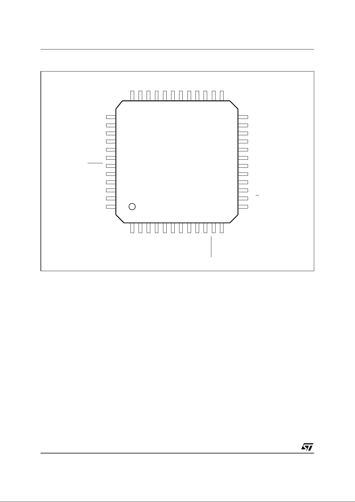
PIN CONNECTIONS
NC
AGND2
V
AV
AUXIN
HM
RESET
TS
TSTD1
DIN
DOUT
NC
NC
D1
D2
CMS
TSTA2
V
D3
D4
V
CMP
D5
TSTA1
D6
NC
2526272829303132333435
37
38
CM
DD
39
40
41
42
43
44
45
46
47
48
24
23
22
21
20
19
18
17
16
15
14
13
NC
AGND1
V
REFN
V
REFP
GPIO0
GPIO1
GPIO2
GPIO3
GPI
RING
M/S
NC
1234567893610 11 12
DD
NC
SCLK
FS
MCM
DV
DGND
XTALOUT
HC1
HC0
PWRDWN
NC
XTALIN (MCLK)
75951-01.EPS
2/21
PIN LIST
Pin Number Name Type Description
2 SCLK O Bit Shift Clock Output , SCLK = Coeff ⋅ FS
3 FS I/O Frame Synchronization Input (Slave)/Output (Master)
4 MCM I Master Clock Mode
5DV
DD
6 DGND I Digital Ground (0V) (see Note1)
7 XTALOUT O Crystal Output
8 XTALIN I Crystal Input
9 HC1 I Hardware Control Input
10 HC0 I Hardware Control Input
11
14 M/
PWRDWN I Power Down Input
S I Master/slave Control Input
15 RING O Ring Detect Output
16 GPI O General Purpose Interrupt Output
17 GPIO3 I/O General Purpose Control Input/Output
18 GPIO2 I/O General Purpose Control Input/Output
19 GPIO1 I/O General Purpose Control Input/ Output
20 GPIO0 I/O General Purpose Control Input/Output
21 V
22 V
REFP
REFN
23 AGND1 I Analog Ground (0V) (see Note1)
26 D6 O ST952 Control Output
27 D5 O ST952 Control Output
28 TSTA1 O Reserved for test
29 V
CMP
30 D4 I Receive Input
31 D3 I Receive Input
32 V
CMS
33 TSTA2 O Reserved for test
34 D2 O Transmit Output
35 D1 O Transmit Output
38 AGND2 I Analog Ground (0V) (see Note1)
39 V
40 AV
CM
DD
41 AUXIN I Receive Auxiliary Analog Input Amplifier
42 HM I Hardware Control Input for Clid/Off-hook
43
RESET I Reset Function to initialize the device
44 TS I Timeslot Control Input
45 TSTD1 I Reserved for Test (must be grounded in normal mode)
46 DIN I Serial Data Input
47 DOUT O Serial Data Output
Note 1 :
Digital and Analog ground must be connected externally together.
I Positive Digital Power Supply
O Positive Reference Voltage
O Negative Reference Voltage
I Common Mode Voltage Input P
I Common Mode Voltage Input S
O Common Mode Voltage Output
I Positive Analog Power Supply
ST75951
75951-01.TBL
3/21

ST75951
PIN DESCRIPTION
1 - Power Supply
1.1 - Power Sup ply
These pins are the positive analog and digital
power supply input (2.7 to 5.25V).
In any case, the AV
or equal to the DV
(5 Pins)
, DVDD)
(AV
DD
voltage must alw ays be higher
DD
voltage (AVDD ≥ DVDD).
DD
A software powerdow n with wake-up on ring detect
is also provided with bit 4 in control register 3.
3.3 - Hardware Control
(HC0, HC1)
These pins are used for hardware/software control
programmation of the device.
1.2 - Analog Ground
( AGND1, AG ND2)
These pins are the ground return of the DAC and
ADC analog section.
1.3 - Digital gr ound
(DGND)
This pin is the ground return of the digital circuitry.
Note : In order to obtain publ ished performances,
the analog A V
and digital DVDD should be decou-
DD
pled with respect to analog ground and digital
ground, respectively. Decoupling capacitors should
be as close as possible to the supplies pins. All
ground must be tied together. In the following section the ground is referred as : GND.
2 - Serial Synchronous Interface
2.1 Data
(DIN, DOU T)
(4 Pins)
Digital data word input/output of the SSI (16 bits
data).
2.2 - Frame Synchronization
(FS)
The frame synchronization is used to indicate that
the device is ready to send and receive data.
The data transfer begins on the falling edge of
frame-sync signal. The frame-SYNC can be generated internally or externally.
2.3 Serial Bit Clock
(SCLK)
Clocks the digital data into DIN and out of DOUT
during the frame synchroniza tion interval. The serial bit clock is generated internally and equal to
MCLK/R (R programmed value in r egister 3) . The
serial bit clock is a multiple of FS.
RESET)
(
(10 Pins)
3 - Control Pins
3.1 - Reset
This pin initializes the internal counters and control
registers to their default value. A minimum low
pulse of 100ns is required to r eset the chip.
PWRDWN)
3.2 - Power-Down
(
This input powers down the entire c hip. In power
down mode the existing internally programmed
state is maintained. When power down is dr iven
high, full operation resumes after 1ms.
3.4 - Hardware Control
(HM)
This pin is used for hardware/software control of
CLID/OFFHOOK function.
(M/
3.5 - Master/Slave
When M/
S = " 1 " the device is in master mode and
S)
FS is generated internally othe rwise the device is
in slave mode and Fs must be provided externally
and equal to SCLK*R / OVER.
3.6 - Timeslot Control
(TS)
When TS = " 0 " t he data are assig ned to the
first timeslot (1st 16 bits after falling edge of FS)
otherwise t he data are on the second tim eslot
(bits 17 to 32).
3.7 - Control
(D5, D6)
These pins transmit the control signals tr ough isolation capacitors to ST952 which converts and
outputs the appropriate control signals.
3.8 - Master Clock Mode
(MCM)
When MCM = " 1 " , we have
FS = Master Clock/[M ⋅ Q ⋅ OVER] otherwise we
have FS = Master Clock/OVER and the M, Q
dividers are bypassed.
4 - General Purpose Input/Output Circuitry
4.1 - GPIO
(4 Pins)
ST75951 offers 4 general purpose Input/Output
pins. The setting of the GPIO configuration is done
through the control register 1 and the signal level
of the GPIO are reflected in the feedback register 2.
At power on the GPIO are programmed as inputs.
In order to take into account the evolution of ST952,
thanks to the control register we will be able to send
a clock signal equal to F0/N (N programmed in
register 2) on GPIO0 and F0 on GPIO3.
When in DAA control hardware mode HM = 1, the
CLID and OFF-HOOK control is done by Pin GPIO1
(CLID) and GPIO2 (OFF- HOOK), otherwise when
HM = 0 then the CLID/OFF-HOOK control is done
by programming the adequate bit in the control
register 3 (Bit 2 , Bit 3, see Table 7).
4/21

ST75951
PIN DESCRIPTION
4.2 - General Purpose Interrupt System
(continued)
(GPI)
The GPI will reflect any change of the GPIO’S
inputs or RING output when non-masked, so the
processor does not need to read the output control
word continuously . G PI level change tells the processor, one of the non-masked input pins level has
changed and he can read the control word. So
GPIO could extend the number of interrupt pins of
the processor.
5 - Ring
This pin is used for the Ring detect but also reports
the Line status, current limit.
6 - Digital Test Pin
(TSTD1)
This pin is reserved for digital test purpose.
7 - Crystal
(XTALIN , XT ALOUT )
These pins must be tied to an external crystal or a
master clock generator (MCLK).
8 - Analog Interface
(12 Pins)
8.1 - DAC and ADC Reference Voltage Output
(V
REFP
, V
REFN
)
These pins provide the positive and negative
reference Voltage used by the 16-bit converters.
The reference voltage, V
between the V
and V
V
REFP
with re s p e ct to V
and V
REFP
should be externally decoupled
REFN
.
CM
8.2 - Common Mode V oltage Output
is the voltage difference
REF ,
outputs.
REFN
(V
CM
)
This output pin is the common mode voltage
(AVDD - AGND)/2 . This output must be decoupled
with re s p e ct to GND.
(V
8.3 - Common Mode V oltage Input
CMP
, V
CMS
These input pins are the common mode voltage for
internal circuitry. They have to be c onnected externally to V
8.4 - Analog Transmit Output
CM
.
(D1 ,D2)
These pins are the output of the fully differential
converted analog signal, modulated at F0
(1MHz < F0 < 1.7MHz).
The digital data IN signal is converted in analog
signals (with (Sin X)/X compensation). Two ranges
of signal amplitude have to be considered ; modem
application with dynamic up to 2.5V
with maxi-
PP
mum performances SNDR = 83dB, voice application with dynamic up to 3.2V
differential
PP
(SNDR = 75dB).
The transmit output stage can be programmed to
+2dB gain, 0db gain, 6dB or infinite attenuation.
8.5 - Analog Receive Inputs
(D3, D4)
These pins are the differential analog inputs. These
analog inputs are presented to the F0 demodulator
and the sigma-delta modulator. The analog input
peak-to-peak differential signal range must be less
than 2.5 V
. The gain of the receive stage is
PP
programmable to 0dB or 6dB.
8.6. - Analog Test Pin
(TSTA1, TSTA2)
These pins are reserved for analog test purpose.
8.7 Analog Auxiliary Receive Inputs
(AUXIN)
This pin is the auxiliary analog input. This analog
input is presented to the analog modulator. The
analog input peak-to-peak signal range must be
less than 1.25 V
. The gain of the rec eive stage
PP
is 0dB.
)
5/21
ST75951
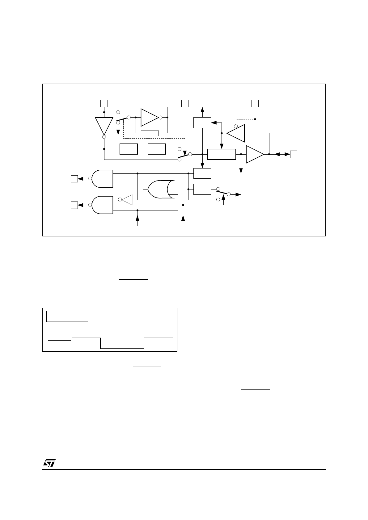
BLOCK DIAGRAM
V
CMSVCMP
AUXIN
41
D3
D4
RING
D1
D2
HIGH
31
PASS
30
FILTER
Bit DR
DETECTOR
MUX
15
F0
35
34
DVDDDGND AVDDAGND1 AGND2 VCMV
40 435 6
2932
F0
LOW
PASS
FILTER
GAIN
GAIN
ATTE
ATTE
2dB
0dB
6dB
INFINITE
23 22 21
GAIN
DAC 1 BIT
First Order
Differential
Switched
Capacitor
Filter
MUX
REFNVREFP
38 39 91011
REFERENCE
VOLTAGE
ANALOG
MODULATOR
2nd ORDER
MODULATOR
RESET PWRDWN
LOW-PASS
(0.425 x Sampling
Frequency)
LOW-PASS
(0.425 x Sampling
Frequency)
HC0 HC1
TSTD1
45
3
2
47
46
SERIAL PORTS
44
AND CONTROL REGISTER
FS
SCLK
DOUT
DIN
TS
CLOCK GENERATOR
STLC75951
28
33 42414 78
TSTA1 TSTA2 M/S MCM XTALIN
2627
D5 D6
(MCLK)
FUNCTIONAL DESCRIPTION
ST75951 is a modem AFE front-end integrating the
modem side of Krypton K951 and fully com patible
to work with ST952.
1 - Transmit Section
The functions included in the transmit section are :
- D/A converter,
- F0 modulator,
- Programmable stage +2dB gain, 0dB gain, 6dB
attenuation or infinite attenuation,
- Transmit Filter including noise shaper and Sinx/x
correction.
The digital bas e Band data (DIN) ar e converte d and
modulate d at F 0 and send di ffere nt ial ly ( D1, D2 ) t o
ST952 through capacitive connection.
2 - Receive Section
The functions included in the rec eive section are :
- Main and Aux inputs,
- Programmable gain 0/6dB,
DAA CONTROL + GPIO
20 19 18 17
XTALOUT HM
GPIO0 GPIO1 GPIO2 GPIO3
- A/D converter,
- F0 demodulator,
- Receive filter.
The analog differential Main input signal (D3, D4)
coming from ST952 is demodulated at F0, goes to
the multiplexer and gain receive block then is digitally converted and output on DOUT which is the
base band data.
Thanks to the multiplexer, we can also process
base band analog signal on AUXIN.
3 - Clock Generator
ST75951 generates all clocks from either a Master
clock input on XTA LIN (MCLK) or a crystal oscillator
connected between XTALIN and XTALOUT.
The bypass of the divider M and Q is selected by
setting the MCM input pin to ’0’.
To be able to provide externally the sampling frequency (Slave mode), M/
S input pin must be set
to ’0’ (see Figure 2).
GPI
16
75951-02.EPS
6/21
ST75951
FUNCTIONAL DESCRIPTION
(continued)
Figure 2
XTALIN
(MCLK) XTALOUT
V
DD
% M % Q
D5
27
F0
D6
26
GPIO1 or CLGPIO2 or OH
4 - Power Down Mode
Tw o PowerD own modes are available in ST 75951
thanks to bit 4 in control register 3.
4.1 - PowerDown Mode 0
If bit 4 is set to ’0’ then when
PWRDWN is set to ’0’
the entire chip is in powerdown mode 0.
Figure 3
MCM
SCLK
2
4 1478
% R
Sync
% OVER
% 2
% 2
Internal Sampling
Frequency
M/S
3
F0 or F0/2
tomer feature associated with a defined GPIO (programmed as input and non-masked).
4.2.1 - Ring Bit and GPIO Bit Masked
In this configuration the processor relies on the
Ring output pin to process the wake-up of the
system and does not need the S S I to be poweredon. The SSI will be put back in operative mode
when
PWRDWN is set to ’1’ (see Figure 4).
FS
75951-03.EPS
REG3 BIT4 = 0
Normal
PWRDWN
4.2 - PowerDown Mode 1
Power Down 0
(100µW)
When bit 4 i s set to ’1’ th en wh en
Normal
PWRDWN is set
to ’0’ the ch ip is in powerd own ex cept th e Ring de tect
circuitry (wake-up on Ring = powerdown mode 1).
The general purpose interrupt is also working in
order to wake-up the system for dedicated cus-
4.2.2 - Ring Bit or GPIO Bit Non-Masked
In this configuration the processor relies on the SS I
to process the wake-up of the system and needs
the SSI to be powered-on.
75951-04.EPS
On an incoming Ring signal or an interrupt coming
thanks to the GPIO, ST75951 will generate an
interrupt on GPI output pin and power-up the SSI,
the processor will be able to read the control register 2 and find out the origine of the interrupt.
After a reading of the register 2, if the processor
does not set high
PWRDWN ST75951 puts b ack
the SSI off in order to save energy (see Figure 5).
7/21

ST75951
FUNCTIONAL DESCRIPTION
Figure 4
REG3 BIT4 = 1
Normal Off-Hook
PWRDWN
Ring
Output Pin
GPI '1'
SSI
ON OFF ON
Figure 5
REG3 BIT4 = 1
PWRDWN
Ring or
non-masked GPIO
Normal Off-Hook
(continued)
Wake-up on Ring
Ring
75951-05.EPS
Wake-up on Interrupt
Ring
GPI
SSI
ON ON
OFF OFF OFFON
5 - Mode of Operation
Thanks to MCM and M/
S programmation pins we
can get the following configuration.
Configuration 1 :
MCM = M/S = ’1’.
ST75951 is in master mode and we have :
FS = FQ / (M x Q x OVER). FS is an output.
(see Figure 6).
Configuration 2 :
MCM = ’1’, M/S = ’ 0 ’.
ST75951 is in slave mode and the processor provides FS = (R x SCLK) OVER. FS is an input
(see Figure 7).
Configuration 3 :
MCM = ’0’, M/S = ’1’.
ST75951 is in master mode and we have :
FS = FQ / (OVER). FS is an output (see Figure 8).
Ring
Processor reads REG2
ST75951 resets Bit GPI
ON
Configuration 4 :
MCM = ’0’, M/
S = ’ 0 ’.
The configuration 4 is equivalent to configuration 3
but the processor generates the FS and control the
phase.
ST75951 is in slave mode and the pr ocessor provides FS = (R x SCLK)/OVER. FS is an input
(see Figure 9).
Configuration 5 :
M/
S = ’ 1 ’. Slave codec 2 : MCM = ’0’, M/S = ’ 0 ’.
Master codec 1 : MCM = ’0’,
This is a dual codec application running on the
same SSI. The master codec has his data in timeslot 0 ( bit 0 t o bit15 ) and the slav e codec has his
data in timeslot 1 (bit 16 to bit 31) thanks to the
programmation of TS (see Figure 10).
75951-06.EPS
8/21

ST75951
FUNCTIONAL DESCRIPTION
Figure 6
fQ = 36.864MHz
18.432MHz
9.216MHz
8
P
R
O
C
E
S
S
O
R
XTALIN
2
SCLK
3
FS
46
DIN
47
DOUT
= fQ / (M x Q x Over)
f
S
M/S
MCM
Figure 7
fQ = 36.864MHz
18.432MHz
9.216MHz
8
P
R
O
C
E
S
S
O
R
XTALIN
2
SCLK
3
FS
46
DIN
47
DOUT
= fQ / (M x Q x Over)
f
S
M/S
MCM
Figure 8
STLC7546
Functional Mode
P
R
O
C
E
S
S
O
R
2
3
46
47
f
XTALIN
SCLK
FS
DIN
DOUT
f
= fQ / Over
S
Q
8
M/S
MCM
(continued)
14
4
44
TS
14
4
44
TS
14
4
44
TS
V
DD
V
DD
GND
GND
V
DD
GND
V
DD
GND
GND
Figure 9
f
Q
8
Figure 10
75951-07.EPS
75951-08.EPS
P
R
O
C
E
S
S
O
R
P
R
O
C
E
S
S
O
R
2
3
46
47
XTALIN
SCLK
FS
DIN
DOUT
= fQ / Over
f
S
8
XTALIN
2
SCLK
3
FS
46
DIN
47
DOUT
8
XTALIN
2
SCLK
3
FS
46
DIN
47
DOUT
M/S
MCM
TS
RESET
43
43
RESET
14
4
44
M/S
MCM
TS
M/S
MCM
TS
GND
GND
GND
Master
Codec 1
14
4
44
Slave
Codec 2
14
4
44
6 - General Purpose Input / Output
ST7 59 51 featur e s 4 GPI O. The GPIO0..3 ar e t raditional inputs/outputs programmed and set thanks to
the control register 1 (mask, input/output) and control
register 2 (output value, static or modulated).
GPIO0 output is dedicated to output F0/N clocks
instead of a static ’1’ if bit 6 in control r egis ter 2 is
set. GPIO3 is dedicated to output F0 clock instead
of a static ’1’ if bit 10 in control register 2 is set (see
Figure 11 and 12).
75951-09.EPS
V
DD
GND
GND
GND
GND
V
DD
75951-10.EPS
75951-11.EPS
9/21

ST75951
FUNCTIONAL DESCRIPTION
Figure 11 :
Figure 12 :
GPIO0 When bit6 = ’1’ in REG2
GPIO0
GPIO0
REG 2 - BIT1
SETTING
GPIO3 When bit10 = ’1’ in REG2
GPIO3
GPIO3
REG 2 - BIT4
SETTING
(continued)
F0/N
F0
GPIO1 and GPIO2 are dedicated input and control
CLID and OFF-HOOK function respectively if the
control input Pin HM is set to ’1’.
Table 2
HM GPIO1 GPIO2 Function
1 0 0 ON-HOOK
1 0 1 OFF-HOOK
11 0 CLID
1 1 1 SPECIAL
HM CL OH Function
0 0 0 ON-HOOK
0 0 1 OFF-HOOK
01 0 CLID
0 1 1 SPECIAL
CL, OH : Bit 2, 3 Reg 3.
Depending of the setting of the Mask bit in control
register 1, any change of non-masked GPIO can
generate an interrupt to the processor thanks to
GPI (General purpose Interrupt).
7 - Operating Modes
Three operating modes controlled either by the
GPIO1 and 2 or by the control register 3 are implemented :
- ON-HOOK,
- OFF-HOOK,
- CLID (Caller ID).
V
DD
PP
V
DD
PP
Figure 13
D5
D6
7.1 - ON-HOOK
During O N-HOOK state no sig nal is se nt by D5, D 6.
D5 = D6 = V
DD
.
Ring
When in ON-HOOK state, the ST952 sends a
1MHz differential signal on D3, D4 when it receives an incoming ringing signal from Tip/Ring.
ST75951 will output on RING Pin the image of the
ring signal (RING Pin is also duplicated in the read
register 2 bit 5) (see Figure 15).
7.2 - OFF-HOOK
Depending on Pin HM status (see Table 2), 2 possibilities are offered to control the device t o go in
OFF-HOOK state.
Figure 14
V
D5
D6
DD
F0
V
DD
F0
D5 and D6 send F0 clock in opposite phase to
ST952.
75951-12.EPS
75951-13.EPS
75951-14.EPS
75951-15.EPS
10/21

ST75951
FUNCTIONAL DESCRIPTION
(continued)
Figure 15
D3
D4
RING
BIT &
OUTPUT
D5
D6
D5 = D6 = V
DD
.
7.3 - Caller ID
Depend ing on P in HM status (see T a ble 2), 2 possibilit ies are offered to control the dev ic e to go in
caller ID state.
F0 clock is send to D5, in caller ID mode the
modulation frequency of ST952 is equal to F0/2, so
the demodulation on the receive signal at D3, D4
is at F0/2 in caller ID mode.
V
CM
V
CM
1MHz
1MHz
8 - Phone Line Monitoring Features
This chipset is intended to be used for a wide range
of application such as modem, answering machine,
telephony on PC, so because the home PSTN
phone line will be shared by several terminals,
information concerning the line status has to be
sent to the host.
As long as there is an alerting signal at D3, D4 Pins,
the ADC converter is saturated and outputs 7FFF
or 8000 at DOUT Pin.
75951-16.EPS
Figure 16
D5
D6
D6 = V
DD
.
Figure 17
FO Output at D5
FO/2 Demod
Control Signal
V
Caller ID Mode Phase Relative Hip
8.1 - Line In Use Checking
Before going OFF-HOOK the modem software can
DD
F0
check that the line is free by setting the CLID mode
and check that the RING Pin/bit output a low pulse.
When in CLID mode if the line is free the ST952 will
output a F0/2, 5V
(see Figure 18).
75951-17.EPS
differential signal on D3, D4
PP
8.2 - Digital Phone Line or Over Loop Current
Limit Detect
When portab le modem plug into digital line, it wil l cause
over loop curre nt during mo dem off-h ook state.
The modem controller should know this condition
and go onhook to avoid the DAA being damaged.
ST952 when OFF-HOOK will determine if the loop
current exceeds the current limit or not ( 160mA).
If we have overcurrent ST952 will continuously
output a low level on RING output Pin.
75951-18.EPS
11/21

ST75951
FUNCTIONAL DESCRIPTION
Figure 18
D5
D6
D3
D4
RING
RING
Figure 19
D5
(continued)
Xms *
Line Free
Line in use, Ring = '1'
V
CM
V
CM
*Xms value is fixed
by ST75952 application
F0
75951-19.EPS
F0
D6
D3
D4
RING
Overcurrent
By programming bit 9,8 = ’ 01’ of c ontrol r egister 3,
we can set ST75951 in ’local analog loop back’ (see
Figure 20).
By programming bit 9, 8 =’ 10’ of c ontrol r egister 3,
we can set ST75951 in ’local digital loop back’ (see
Figure 21).
F0
F0
75951-20.EPS
Figure 209 - Analog / Digital Loop Back Test
LOW-PASS
2nd ORDER
MODULATOR
(0.425 x Sampling
Frequency)
LOW-PASS
(0.425 x Sampling
Frequency)
DOUT
DIN
75951-21.EPS
12/21

ST75951
FUNCTIONAL DESCRIPTION
(continued)
Figure 21
AUXIN
41
F0 or F0/2
D3
D4
RING
D1
D2
31
30
15
35
34
HIGH
PASS
FILTER
Bit DR
DETECTOR
MUX
F0 or F0/2
ATTENUATION
0dB/6dB/Infinite
LOW
PASS
FILTER
10 - Host Interface
Table 3
HC1 HC0 LSB 2nd FS Mode Description
000 no
001 yes
01x no
1xx yes
Software mode,
data transfer only
Software mode,
data xfer + control xfer
Hardware mode,
data transfer only
Hardware mode,
data + control transfer
The host interface is a Serial Synchronous Interface (FS, SCLK, DOUT, DIN).
Tw o modes of serial transfer are available and are
selected via pins HC0 and HC1.
First mode is a software mode control (15 bits
transmit data and 16 bits receive data). In this mode
ST75951 is completely controlled through the SSI,
the access of control register is done by managing
the LSB of the transmit data word.
Figure 22 :
WRITE REG n , READ default REG 2
1/2 Sampling Period
MUX
FIRST ORDER
DIFFERENTIAL
CAPACITOR FILTER
GAIN
DAC 1 BIT
SWITCHED
ANALOG
MODULATOR
Second mode is a hardware mode control (16bits
data transmit and receive). In this mode the ac cess
of control register is done via dynamic setting of
Pins HC0 and HC1 (s ee Table 3).
The bit 15 of the control word is used to do a read
only or a read and write of control register
(bit 15 = 1 Read only, bit 15 = 0 Read & Write).
11 - Control Registers
This section defines how to handle the 4 registers
implemented in ST75951.
11.1 - Write / Read Operation
(D15 = 0)
This is a one sampling frequenc y period duration
operation, where the 16-bit word sent from t he host
on DIN, contains the write qualifier, the address
register and the data field.
Contemporaly ST75951 ouptuts on DOUT the
register 2 value (GPIO) (see Figure 22).
Sampling Period
75951-22.EPS
FS
DI
D0
HC0
HC1
D15
DATA WORD INPUT @regN+cont.word
DATA WORD OUTPUT
0
REGISTER 2 VALUE
0110
75951-23.EPS
13/21

ST75951
FUNCTIONAL DESCRIPTION
(continued)
Figure 23
1/2 Sampling Period
FS
DI
D0
HC0
HC1
DATA WORD INPUT @regN (read only)
DATA WORD OUTPUT
10
1 1.2 - Read Operation
Sampling Period
D15
1
REGISTER 2 VALUE
(Register n) (D15 = 1)
This is a two sampling frequency period duration
operation, where a first 16 bit word sent from the
host on DIN, contains the read qualifier and the
address register (register n).
Contemporaly ST75951 ouptuts on DOUT the register 2 (GPIO) while the address field is decoded.
Then a second read operation with the default
address (register 2) is sent to the device. At t hat
Figure 25
SCLK
Sampling Period, (128, 192, 256, 320 or 384)
1/2 Sampling Period
FS
D0D1
0
D0
D0D1
1
D0
D0
D0
D0
D0
HC1 = 0
HC0 = 0
HC1 = 0
HC0 = 1
HC1 = 1
HC0 = X
DIN
DOUT
DIN
DOUT
DIN
DOUT
DIN
DOUT
D15
DATA WORD INPUT (15 BITS)
D15
DATA WORD OUPUT (16 BITS)
D15
DATA WORD INPUT (15 BITS)
D15
DATA WORD OUPUT (16 BITS)
D15
DATA WORD INPUT (16 BITS)
D15
DATA WORD OUPUT (16 BITS)
D15
DATA WORD INPUT (16 BITS)
D15
DATA WORD OUPUT (16 BITS)
1/2 Sampling Period
FS
DATA WORD OUTPUT
10
Sampling Period
1
REGISTER N VALUE
D15
@reg2 (read only)DATA WORD INPUT
time ST75951 outputs on DOUT the register n
value (see Figure 23, 24 and 25).
Figure 24
16 Bits Control Word Format
R/W ad2 ad1 ad0 d11...............d0
D15 D0
(Only if Control Mode Selected)
D15
D15
D15
CONTROL WORD (16 BITS)
D15
REGISTER VALUE (16 BITS)
D15
CONTROL WORD (16 BITS)
D15
REGISTER VALUE (16 BITS)
D0
D0
D0
D0
D15
D15
D15
D15
D15
D15
01
75951-24.EPS
75951-25.EPS
75951-26.EPS
14/21

ST75951
FUNCTIONAL DESCRIPTION
Table 4 :
Bit15 Bit14 Bit13 Bit12 Bit11 Bit10 Bit9 Bit8 Bit7 Bit6 Bit5 Bit4 Bit3 Bit2 Bit1 Bit0 Function
Control Register 0 : AFE Setting
0 0 0 0 Main Receive input (INI)
0 0 0 1 Auxil. Receive input
0 0 0 0 0dB Receive Gain (INI)
0 0 0 1 +6dB Receive Gain
0 0 0 0 0 0 OVER = 320 (INI)
0 0 0 0 0 1 OVER = 384
0 0 0 1 0 1 OVER = 128
0 0 0 1 1 0 OVER = 192
0 0 0 1 1 1 OVER = 256
0 0 0 0 0 - Infin. attenuation XMIT (INI)
0 0 0 0 1 +2dB gain XMIT
0 0 0 1 0 6dB attenuation XMIT
0 0 0 1 1 0dB gain XMIT
000 0 M = 1
0 0 0 1 M = 2 (INI)
000000 Q = 3
000001 Q = 6 (INI)
000010 Q = 7
000011 Q = 8
000100 Q = 4.5
000101 Q = 5.5
000110 Q = 6.5
000111 Q = 7.5
(continued)
Table 5 :
Bit15 Bit14 Bit13 Bit12 Bit11 Bit10 Bit9 Bit8 Bit7 Bit6 Bit5 Bit4 Bit3 Bit2 Bit1 Bit0 Function
Table 6 :
Bit15 Bit14 Bit13 Bit12 Bit11 Bit10 Bit9 Bit8 Bit7 Bit6 Bit5 Bit4 Bit3 Bit2 Bit1 Bit0 Function
Note :
Control Register 1 : GPIO Setting, Ring Bit
0 0 1 Di3 Di2 Di1 Di0 DIR. ’0’ = (Inp INI), 1 = Out
0 0 1 MR M3 M2 M1 M0 MASK for INT. GPI ’0’ masked
DR Digital Ring ’1’ on, ’0’ off (INI)
(INI), ’1 ’ unmaske d
Control Register 2 : GPIO / RING Output Setting
0 1 0 G3 G2 G1 G0 GPIOx output setting, read
0 1 0 RG Read only, Ring
0 1 0 S GPIO3 ’0’ In static Value (INI)
0 1 0 x x 0 GPIO0 In static Value (INI)
0 1 0 0 0 1 GPIO0 Modulate at F0
0 1 0 0 1 1 GPIO0 Modul. at F0/2
0 1 0 1 0 1 GPIO0 Modul. at F0/4
0 1 0 1 1 1 GPIO0 Modul. at F0/8
GPI is in "high" state, any chang e on one Gx or RG non-masked put GPI in "low" state, one r ead on this register (@010) put GPI in
"hight" state.
input
if set GPIO3 modulated at F0
15/21

ST75951
FUNCTIONAL DESCRIPTION
Table 7 :
Bit15 Bit14 Bit13 Bit12 Bit11 Bit10 Bit9 Bit8 Bit7 Bit6 Bit5 Bit4 Bit3 Bit2 Bit1 Bit0 Function
Control Register 3 : Clock / configuration setting
0 1 1 OH CL Software value (HM = 0)
0 1 1 0 Normal operation (INI)
0 1 1 1 PowerDown with wake-up
0 1 1 0 Transmit modulated (INI)
0 1 1 1 Transmit not modulated
0 1 1 0 0 SCLK = MCLK (R = 1)
0 1 1 0 1 SCLK = MCLK/2 (R = 2) (INI)
0 1 1 1 0 SCLK = MCLK/4 (R = 4)
0 1 1 1 1 Reserved
0 1 1 0 0 Normal mode (INI)
0 1 1 0 1 Analog loop back
0 1 1 1 0 Digital loop back
0 1 1 1 1 Reserved
01100 Normal mode (INI)
01101 Reserved
01110 TSTD1 Pin = PCLK output
01111 TSTD1 Pin = PCLK input
(continued)
on ring or non-masked GPIO
Below you’ll find a table giving different programmation for achieving all common V.34 baud rate with
ST75951 working with an external crystal f
= 36.864 MHz. The 8kHz could be used for voice processing
Q
and the 16kHz for the 56K (V.pcm).
Table 8
Baud Rate F
3429 13714 .29 192 2 7 1316571
3000 12000 256 2 6 1536000
3490 10472 .73 320 2 5.5 16 75636
3429 10285 .71 256 2 7 1316571
2400/3200 9600 320 2 6 1536000
3000 9000 256 2 8 1152000
2953 8861.54 320 2 6.5 1417846
2743 8228.57 320 2 7 1316571
2400 7200 320 2 8 1152000
S
16000 192 2 6 1536000
8000 384 2 6 1536000
Over M Q F0
In any cases attention must be paid to have F0 between 1MHz and 1.7 MHz , optimum value beeing 1.5MHz.
The modulator and demodulator frequency F0 = OVERSAMPLING FREQUENCY / 2.
When MCM = ’ 0’, we hav e OVERSAMPLING FR E Q U E N C Y = MCLK and F0 = MCLK / 2 SCLK = MCLK / R
(see clock block diagram).
Table 9 :
(eg : with R = 4)
fS (kHz) M Q Over MCLK (MHz) F0 (MKz) SCLK (kHz)
8 X X 384 3.072 1.536 768
9.6 X X 320 3.072 1.536 768
9.6 X X 256 2.4576 1.2288 614.4
16 X X 192 3.072 1.536 768
16/21

ELECTRICAL SPEC I F ICATION
Unless otherwise noted, Electrical charac teris tics are specified over the operating range.
Ty pical value are given for V
= 3.3V, T
DD
= 25°C. Initial value MCLK external = 3.072MHz.
AMB
ST75951
Absolute Maximum Rating
(AGND = DGND = 0V, all v oltages with respect to 0V)
Symbol Parameter Value Unit
AV
DV
Analog Power Supply -0.3, 6.0 V
DD
Digital Power Supply -0.3, 6.0 V
DD
II Input Current per Pin -10, +10 mA
Output Current per Pin -20, +20 mA
I
O
Analog Input Voltage -0.3, 6 V
IA
Digital Input Voltage -0.3, 6 V
ID
Digital Input Voltage at GPIO 5.25 V
Operating Temperature 0, +70 °C
oper
Storage Temperature - 40, +125 °C
stg
Maximum Power Dissipation 200 mW
tot
V
IDGPIO
T
T
P
V
V
Warning : Operation beyond these limits may result in permanent damage to the device. Norm al operation
is not guaranteed at these extremes.
= 0 to 70°C unless otherwise specified)
Dc Characteristics
(T
amb
Power Supply And Common Mode Voltage
Symbol Parameter Min. Typ. Max. Unit
V
I
DVDD
I
AVDD
I
I
DLP R
V
Note 1 :
Supply Voltage 2.7 3.3 5.25 V
DD
Digital Supply Current 6 8 mA
Analog Supply Current 9 12 mA
Low Power mode (Hardware control PWRDWN Pin) @ 25°C 10 µA
DLP
Low Power mode (S oftware control with wake-up on Rin g) @ 25° C 30 100 µA
Common Mode Voltage Output (see note 1) AVDD/2-5% AVDD/2+5% V
CM
V
output voltage current must be D C (<10 µA) If dynamic lo ad exists, the VC M output must be buffered or the perfor m ances of
CM
ADCs and DACs will be degraded.
75951-02.TBL
75951-03.TBL
Digital Interface
Symbol Parameter Min. Typ. Max. Unit
V
V
V
V
I
LEAK
I
High Level Input Voltage DVDD-0.5 V
IH
Low Level Input Voltage -0.3 0.5 V
IL
High Level Output Voltage (I
OH
Low Level Output Voltage (I
OL
= +2mA) DVDD-0.5 V
LOAD
= -2mA ) 0.3 V
LOAD
Input Leakage Current -1 1 µA
Input Leakage Current (XTALIN Pin when MCM = 1) -25 25 µA
XIN
75951-04.TBL
17/21

ST75951
ELECTRICAL SPEC I F ICATION
(continued)
Analog Interface
(typical value are given for A V
= DVDD = 3.3V , T
DD
Symbol Parameter Test Conditions Min. Typ. Max. Unit
V
V
DIFF IN
V
ADO OUT
V
DIFF OUT
V
OFF OUT
R
R
Differential reference voltage output
REF
V
REF
= (V
REFP
- V
REFN
)
Differential Input Voltage
[D3 - D4] ≤ 2 x V
REF
A/D Modulato r Output DC Offset Vol tage See Figure 26 -50 50 mV
Differential Output Voltage [D1 - D2] XMIT = 0dB
XMIT= 2dB
Differential Output DC Offset Voltage Input code = 0000h -50 50 mV
Input Resistance (D3, D4) 40 kΩ
IN
Output Resistance (D1, D2) 4 kΩ
OUT
R
Load Resistance (D1, D2) 10 kΩ
L
C
Load Capacitance (D1, D2) 20 pF
L
Res Converter Resolution See Note 2 16 Bit
DNL Differential Non Linearity See Note 2 -0.9 0.9 Bit
GTX Channel Gain at f
+ 1kHz -0.5 0.5 dB
0
Ripple Ripple in Band 0 to 0.425 * f
StopB Stop Band Attenuation f
± 0.5 * f
0
SNDR Signal / Noise + Distortion at - 5dBr XMIT = 0dB, see Note 1
XMIT = 2dB
DR Dynamic Range f = 1kHz, XMIT ATTE = 0dB, see Note 1,
Measured over the full 0 to Fs/2 with
-20dBr input and extrapoled to full scale
GRX Receive Gain (Rx gain set to 0 dB) -1 0 +1 dB
PSRR Power supply rejection ratio f = 1kHz, V
Notes :
1. Thes e param eters are valid for transmit and receive channels.
2. This specification is guaranteed by characterization, not production testing.
3. Tr ansm i t chan nel s measured in baseband without modulation.
= 25oC. Measurement band = 0 to 0.425 x fS)
amb
1.18 1.25 1.32 V
2.5 V
2.5
3.2
, see Notes 2 & 3 ±0.2 dB
S
S
-70 dB
80
74
85 dB
= 200mVPP, see Note 1 40 dB
AC
V
V
PP
PP
PP
dB
dB
75951-05.TBL
Figure 26
18/21
ST75951
D3
D4
31
30
VCM
75951-27.EPS

ST75951
ELECTRICAL SPEC I F ICATION
(continued)
Serial Channel Timing
(Reference level V
= 0.8V, VIH = DVDD-0.5V, Vol = 0.4V, VOH = DVDD-0.5V, V
IL
Symbol Parameter Min. Typ. Max. Unit
1 SCLK Period 300 ns
2 SCLK Width Low 150 ns
3 SCLK Width High 150 ns
4 SCLK Rise Time 10 ns
5 SCLK Fall Time 10 ns
6 FS Set-up 100 ns
7 FS Hold 100 ns
8 Din set-up 50 ns
9 Din Hold 0 ns
10 D
Valid 20 ns
OUT
11 HC0, HC1 Set-up 20 ns
12 FS to SCLK Delay 0 50 ns
Figure 27 :
MCLK
SCLK
FS
Timing Diagram (R = 4)
12
6 7
3 2
4
5
= 5V)
BUS
1
89
75951-06.TBL
DIN
DOUT
HC0, 1
MSB
10
MSB
11
75951-28.EPS
19/21

ST75951
TYPICAL APPLICATION
Tip
W
10
SMTPA
270
Ring
22k
47nF
47nF
W
22k
W
D5
D4
Q1
47k
47k
Q5
W
12V
Q2
W
Q3
F
m
15
W
39
D7
D6
Q4
W
620
W
82k
1mF
82
1nF
47k
W
W
100nF
4.7mF
100nF
23
24
11
10
17
16
20
22
21
19
15
14
18
25
32
3
9
6
ST952
LINI
GAIN
OHC
COM
TER1
TER2
RIN
LINE
IDI
IDG
IDC
VDR
VDREF
IREF
SET
LCOM
LCOM
TOFF
D1
D2
D3
D4
D5
D6
LIM2
LIM1
AOUT
AIN
30
31
1
2
4
5
10
m
F
100nF
100nF
10
m
F
10
m
F
100nF
7
8
27
1mF
26
35
34
31
30
27
26
GPI
16
V
21
V
39
V
22
V
32
V
29
AUXIN
41
TSTA1
28
TSTA2
33
TSTD1
45
HM
18
XTALIN
8
XTALOUT
7
D1
D2
D3
D4
D5
D6
REFP
CM
REFN
CMS
CMP
ST75951
RESET
PWRDWN
AGND2
AGND1
MCLK
SCLK
FS
DIN
DOUT
HC1
M/S
MCM
HC0
GPIO0
GPIO1
GPIO2
GPIO3
DV
AV
DGND
TS
8
2
P
3
R
46
47
43
11
O
C
E
S
S
O
R
9
DV
14
DD
DV
4
DD
DV
10
DD
44
20
19
100nF
18
17
22mF
22mF
100nF
DV
AV
DD
DD
5
DD
40
DD
38
23
6
75951-29.EPS
20/21

PACKAGE MECHANICAL DATA
48 PINS - THIN PLASTIC QUAD FLAT P A CK (TQFP)
48 37
1
e
36
ST75951
A
A2
A1
0,10 mm
.004 inch
SEATING PLANE
B
c
Dimensions
E
E3
E1
12
13 24
D3
D1
D
25
L1
L
K
0,25 mm
.010 inch
GAGE PLANE
Millimeters Inches
Min. Typ. Max. Min. Typ. Max.
A 1.60 0.063
A1 0.05 0.15 0.002 0.006
A2 1.35 1.40 1.45 0.053 0.055 0.057
B 0.17 0.22 0.27 0.007 0.009 0.011
C 0.09 0.20 0.004 0.008
D 9.00 0.354
D1 7.00 0.276
D3 5.50 0.216
e 0.50 0.0197
E 9.00 0.354
E1 7.00 0.276
E3 5.50 0.216
L 0.45 0.60 0.75 0.018 0.024 0.030
L1 1.00 0.039
K0
Information furnished is believed to be accurate and reliable. However, STMicroelectronics assumes no responsibility for the
consequences of use of such information nor for any infringement of patents or other rights of third parties which may result from
its use. No licence is granted by implicat ion or otherwise under any patent or patent rights of STMicroelec tronics. Specifications
mentioned in this publication are subject to change without notice. This publication supersedes and replaces all information
previously supplied. STMicroelectronics products are not authorized for use as critical components in life support devices or syst em s
without express written approv al of STMi cr oelec troni cs.
Purchase of I
Rights to use these components in a I
Australia - Brazil - Canada - China - France - Germany - Italy - Japan - Korea - Malaysia - Malta - Mexico - Morocco - The Netherlands
Singapore - Spain - Sweden - Switzerland - Taiwan - Thailand - United Kingdom - U.S.A.
The ST logo is a registered trademark of STMicroelectronics
© 1999 STMicroelectronics - All Rights Reserved
2
C Components of STMicroelectronics, conveys a license under the Philips I2C Pate n t .
2
the I
C Standard Specifications as defined by Phili ps.
STMicroelectronics GROUP OF COMPANIES
2
C system, is granted provided that the system conforms to
http://www.st.com
o
(Min.), 7o (Max.)
21/21
PM-5B.EPS
5B.TBL
 Loading...