

ST75185
MULTIPLE RS-232 DRIVERS AND RECEIVERS
June 2000
■ MEETS ANDEXCEEDSTHE
REQUIREM EN TSOFEIA/TIA-232-EAND
ITUV.28STANDARD
■
SINGLECHIPWITHEASYINTERFACE
BETWEEN UARTAND SERIALPORT
CONNECTOROFIBMPC/AT AND
COMPATIBLES
■ DESIGNEDTO SUPPORTDATARATESUP
TO120 Kbps
■ PINOUT COMPATIBLEWITHST75C185
DESCRIPTION
The ST75185 contains three drivers and five
receivers. The pinout matches the DB9S
connector design in order to decrease the part
count, reducethe boardspace requiredand allow
easy interconnection of the UART and serialport
connectorof IBM PC/AT and compatibles. The
bipolar circuits and processing of the ST75185
provides a rugged low-cost solution for this
function at the expense of quiescent power and
external passive components relative to the
ST75C185.
The ST75185 complies with the requirements of
the EIA/TIA 232-E and ITU (formallyCCITT) v.28
standards. These standards are for data
interchange between a host computer and
peripheral at signallingrates up to 20k-bits/s.The
switchingspeeds of the ST75185 are fast enough
to support rates up to 120K-bits/s with lower
capacitive loads (shorter cables). Interoperability
at the higher signalling rates cannot be assured
unless the designer has design control of the
cable and the interface circuits at the both ends.
For interoperability at signalling rates to 120
K-bits/s, use of EIA/ITA-423-B (ITU v.10) and
EIA/ITA-422-B (ITU v.11) standards are
recommended.
The ST75185 is characterized for operation over
the range of 0
o
Cto70oC.
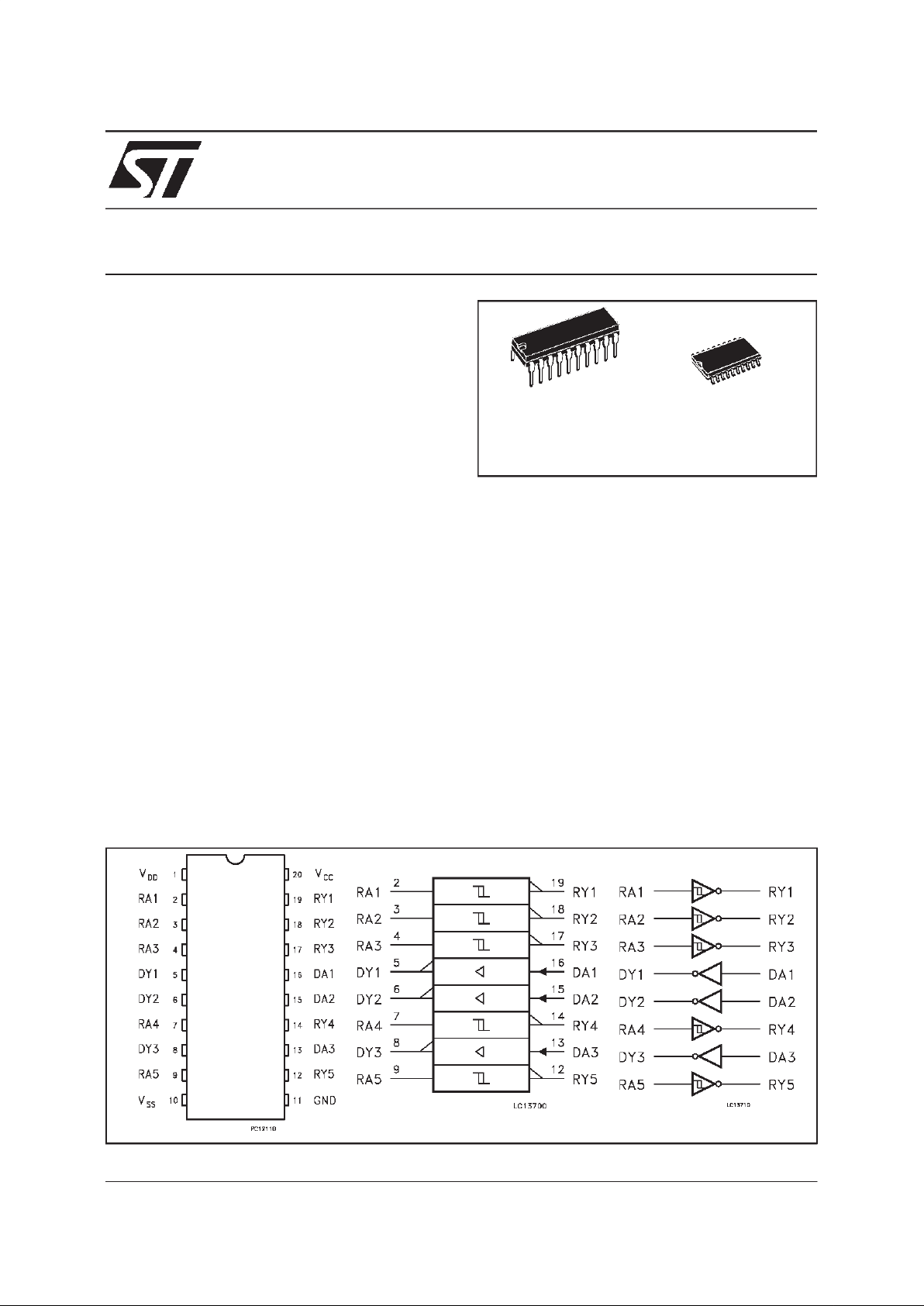
PIN CONNECTION IEC LOGICSYMBOL AND LOGICDIAGRAM
ORDERCODES :
ST75185CN ST75185CD
D
(Micro Package)
N
(PlasticPackage)
1/12
ORDERCODES
Typ e T emperature Range Packag e Commen ts
ST75185CN 0 to 70
o
C DIP-20 20 parts per tube / 50 tubesper box
ST75185CD 0 to 70
o
C SO-20 (Tube) 40 parts per tube / 25 tubesper box
ST75185CDR 0 to 70
o
C SO-20 (Tape &Reel) 1000 parts per reel
PIN DESCRIPTION
PIN No SYMBOL NAME AND F UNCTION
1V
DD
Supply Voltage (+12V)
2 RA1 First Receiver Input
3 RA2 Second Receiver Input
4 RA3 Third Receiver Input
5 DY1 First Driver Output
6 DY2 Second Driver Output
7 RA4 FourthReceiver Input
8 DY3 Third Driver Output
9 RA5 Fifth Receiver Input
10 V
SS
Supply Voltage (-12V)
11 GND Ground
12 RY5 Fifth Receiver Output
13 DA3 Third Driver Input
14 RY4 Fourth Receiver Output
15 DA2 Second Driver Input
16 DA1 First Driver Input
17 RY3 Third Receiver Output
18 RY2 Second Receiver Output
19 RY1 First Receiver Output
20 V
CC
Supply Voltage (+5V)
ST75185
2/12
ABSOLUTE MAXIMUM RATINGSOVER OPERATINGFREE-AIR TEMPERATURE RANGE
(unlessotherwise specified)
Symb o l P ara meter Val u e Un i t
V
DD
Supply Voltage (Note 1) 15 V
V
SS
Supply Voltage (Note 1) -15 V
V
CC
Supply Voltage (Note 1) 10 V
V
I
Input Voltage Range (DRIVER) -15 to 7 V
V
I
Input Voltage Range (RECEIVER) -30 to 30 V
V
O
Output Voltage Range (DRIVER) -15 to 15 V
I
O
Receiver Low Level Output Current 20 mA
P
D
Continuous Total Power Dissipation See Dissipation Rating Table
T
A
Operating Free-Air Temperature Range 0 to 70
o
C
T
stg
Storage Temperature Range -65 to +150
o
C
T
L
Lead Temperature 1.6mm from case for 10 sec 260
o
C
AbsoluteMaximumRatingsarethose values beyond whichdamage tothedevicemayoccur. Functionaloperationunderthese condition isnotimplied.
NOTE1:Allvoltage arewithrespecttothenetworkground terminal.
DISSIPATION RATING TABLE
Packag e Pow er Rating
at T
A
≤
25
o
C
Derati n g F actor
above TA=25oC(*)
Power Rating
at T
A
≤
70
o
C
MICROPACKAGE (D) 1125 mW 9.0 mW/
o
C 720 mW
DIP (N) 1150 mW 9.2 mW/
o
C 736 mW
(*)This is thereverse of the traditional junction-case thermal resistance R
tJ-C
RECOMMENDED OPERATINGCONDITIONS
Symb o l P a rameter Mi n Max Uni t
V
DD
Supply Voltage 7.5 15 V
V
SS
Supply Voltage -7.5 -15 V
V
CC
Supply Voltage 4.5 5.5 V
V
IN
Driver Input Voltege 0 V
CC
V
I
OH
High Level Output Current DRIVER -6 mA
RECEIVER -0.5
I
OL
Low Level Output Current DRIVER 6 mA
RECEIVER 16
T
A
Operating Free-Air Temperature 0 70
o
C
ST75185
3/12

SUPPLYCURRENTS
Symbol Parameter Test C ondition s Value Unit
V
DD
V
SS
Min. Typ. Max.
I
DD
Supply Current from V
DD
9-9
No load.
All inputs at
1.9V
15
mA
12 -12 19
15 -15 25
9-9
No load.
All inputs at
0.8V
4.5 mA
12 -12 5.5
15 -15 9
I
SS
Supply Current from V
SS
9-9
No load.
All inputs at
1.9V
-15
mA
12 -12 -19
15 -15 -25
9-9
No load.
All inputs at
0.8V
-3.2 mA
12 -12 -3.2
15 -15 -3.2
I
CC
Supply Current from V
CC
No load. All inputs at 5V
V
CC
=5V
30 mA
DRIVERELECTRICALCHARACTERISTICS OVER OPERATINGFREE-AIR TEMPERATURE
RANGE (V
DD
= 9V, VSS= -9V,VCC=5V, unlessotherwise specified)
Symbol Parameter Test C ondition s Value Unit
Min. Typ. Max.
V
OH
High Level Output Voltage
V
IL
=0.8V RL=3KΩ
(See Figure 1)
6 7.5
V
V
OL
Low Level Output Voltage (Note 3)
V
IH
=1.9V RL=3KΩ
(See Figure 1)
-7.5 -6 V
I
IH
High Level Input Current VI= 5 V (See Figure 2) 10
µ
A
I
IL
Low Level Input Current VI= 0 V (See Figure 2) -1.6 mA
I
OS(H)
High Level Short Circuit Output Current
(Note 4)
VIL=0.8V VO=0V
(See Figure 1)
-4.5 -12 -19.5 mA
I
OS(L)
Low Level Short Circuit Output Current VIH=2V VO=0V
(See Figure 1)
4.5 12 19.5 mA
R
O
Output Resistance VDD=VSS=VCC=0V
V
O
= -2 to 2 V (Note 5)
300
Ω
NOTE3:
The algebraic convention, where the more positive (less negative) limitisdesignated as maximum, isused in this datasheet for logic levels only
(e.g.if-10V isa maximum,thetypicalvalue isa morenegative voltage).
NOTE4:
Outputshortcircuitconditions must mantainthetotal power dissipation below absolute maximumratings.
NOTE5: Testcond ition s arethose specifiedby EIA-232-Eand aslisted above.
ST75185
4/12

RECEIVERELECTRICAL CHARACTERISTICS OVER OPERATING CONDITIONS
Symbol Parameter Test C ondition s Value Unit
Min. Typ. Max.
V
T+
Positive Going Threshold Voltage (See Figure 6) 2.2 2.4 V
V
T-
Negative Going Threshold Voltage TA=25oC (See Figure 6) 0.75 0.97 V
V
hys
Input Hysteresis (VT+-VT-) 0.5
V
V
OH
High Level Output Voltage IOH= -0.5mA VIH= 0.75 V 2.6 4 5
V
Inputs Open 2.6
V
OL
Low Level Output Voltage VI=3V IOL= 10 mA 0.2 0.45 V
I
IH
High Level Input Current VI= 25 V (See Figure 6) 3.6 8.3 mA
V
I
= 3 V (See Figure 6) 0.43
I
IL
Low Level Input Current VI= -25 V (See Figure 6) -3.6 -8.3 mA
V
I
= -3 V (See Figure 6) -0.43
I
OS
Short-Circuit Output Current VI=0V VO=0V
(See Figure 5)
-3.4 -12 mA
Alltypicalvalues areatTA=25oC,VCC=5V,VDD=9VandVSS=-9V
DRIVERSWITCHING CHARACTERISTICS
(V
DD
= 12V, VSS=-12V, VCC=5V TA=25oC)
Symbol Parameter Test C ondition s Value Unit
Min. Typ. Max.
t
PLH
Propagation Delay Time, Low to High
Level Output
R
L
=3to7KΩ CL=15pF
(See Figures 3, 4)
315 500
ns
t
PHL
Propagation Delay Time High to Low
Level Output
R
L
=3to7KΩCL=15pF
(See Figures 3, 4)
75 175 ns
t
TLH
Transition Time Low to High Level
Output
R
L
=3to7KΩ CL=15pF
(See Figures 3, 4)
60 100 ns
R
L
=3to7KΩ CL=2500pF
(Note 6, See Figure 3, 4)
1.7 2.5 µs
t
THL
Transition Time High to Low Level
Output
R
L
=3to7KΩCL=15pF
(See Figure 3, 4)
40 7.5 ns
R
L
=3to7KΩ CL=2500pF
(Note 6, See Figure 3, 4)
1.5 2.5 µs
NOTE6: Measured between-3Vand3V pointsofoutputwaveform(EIA-232-Econditions), allunusedinputsare tied.
RECEIVER SWITCHINGCHARACTERISTICS
(V
DD
= 12V, VSS= -12V,VCC=5V TA=25oC)
Symb ol Parameter Test C o n dit i ons Val ue Unit
Min. Typ. M ax.
t
PLH
Propagation Delay Time, Low to High
Level Output
R
L
=5KΩ CL=50pF
(See Figure 6)
400 1000
ns
t
PHL
Propagation Delay Time High to Low
Level Output
R
L
=5KΩCL=50pF
(See Figure 6)
70 150 ns
t
TLH
Transition Time Low to High Level
Output
R
L
=5KΩ CL=50pF
(See Figure 6)
200 525 ns
t
THL
Transition Time High to Low Level
Output
R
L
=5KΩ CL=50pF
(See Figure 6)
20 60 ns
ST75185
5/12

APPLICATION CIRCUITS
To CPU
RI
5
1
2
3
4
9
6
7
8
GND
DCD
DSR
RXD
RTS
TXD
CTS
DTR
Rin1
Rin5
Rin4
Rin3
Rin2
Dout3
Dout2
Dout1
Rout1
Rout5
Rout4
Rout3
Rout2
Din1
Din3
Din2
1
Vss
GND
2
Vcc
Vdd
ST75185
20
19
9
7
6
5
4
3
14
13
8
10
18
11
12
17
16
15
Vcc
+5V
Vdd
+12 V
Vss
-12V
Dib9 Serial Port Connector
RS232 LEVEL
TTL LEVEL
PC Serial Port
100nF
100nF
100nF
C
L
CL
CL
UART
(16550)
DCD 38
DSR 37
DTR 33
TXD 11
RXD 21
CTS 36
RTS 32
RI 39
FIGURE1: Driver Test Circuitfor VOH,VOL,
I
SO(H)
and I
SO(L)
FIGURE2: Driver Test Circuitfor IIHandI
IL
ST75185
6/12

FIGURE3:
DriverTest Circuit
FIGURE4:
Driver VoltageWaveforms
FIGURE5: Receiver Test Circuit for I
OS
FIGURE6: Receiver Test Circuit for VT,VOH,V
OL
NOTEA:Thepulsegenerator has thefollowingcharacteristics: t
W
=25µs,PRR= 20KHz,ZO=50Ω,tr=tf<50ns.
NOTEB:C
L
includesprobeandjigcapacitance.
FIGURE7: Receiver Test Circuit FIGURE8: Receiver VoltageWaveforms
ST75185
7/12

DriverVoltage Transfer Characteristics
DriverShort Circuit OutputCurrent vs Free-Air
Temperature
DeviceSupply Current vsTemperature
DriverOutput Current vs OutputVoltage
DriverOutput Slew Rate vs LoadCapacitance
ReceiverThresholdvs Temperature
ST75185
8/12

ReceiverThresholdvs Supply Voltage
+V
-V
ST75185
Output
Lowimpedance
in the power off
condition.
ST75185
Output
Outputshorted
to ±15V
DD
SS
APPLICATION INFORMATION: DIODESON POWERSUPPLY
Diodes placed in series with the V
DD
and VSSleads protect the ST75185 in the fault condition in which
the devices output are shorted to±15V and the power supplies are at low state and provide
low-impedancepath toground (see Figure below)
ST75185
9/12

DIM.
mm inch
MIN. TYP. MAX. MIN. TYP. MAX.
a1 0.254 0.010
B 1.39 1.65 0.055 0.065
b 0.45 0.018
b1 0.25 0.010
D 25.4 1.000
E 8.5 0.335
e 2.54 0.100
e3 22.86 0.900
F 7.1 0.280
I 3.93 0.155
L 3.3 0.130
Z 1.34 0.053
P001J
Plastic DIP-20 (0.25) MECHANICAL DATA
ST75185
10/12

DIM.
mm inch
MIN. TYP. MAX. MIN. TYP. MAX.
A 2.65 0.104
a1 0.10 0.20 0.004 0.007
a2 2.45 0.096
b 0.35 0.49 0.013 0.019
b1 0.23 0.32 0.009 0.012
C 0.50 0.020
c1 45 (typ.)
D 12.60 13.00 0.496 0.512
E 10.00 10.65 0.393 0.419
e 1.27 0.050
e3 11.43 0.450
F 7.40 7.60 0.291 0.299
L 0.50 1.27 0.19 0.050
M 0.75 0.029
S 8 (max.)
P013L
SO-20 MECHANICAL DATA
ST75185
11/12

Information furnished isbelieved to be accurate and reliable. However, STMicroelectronics assumes no responsibility forthe consequences
of use of such information nor for any infringement of patents or other rights of third parties which may result from its use. No license is
granted by implication or otherwise under any patent or patent rights of STMicroelectronics. Specification mentioned in this publication are
subject tochange withoutnotice. Thispublication supersedes andreplaces all informationpreviously supplied. STMicroelectronics products
are not authorized for use as critical components in lifesupport devices or systems withoutexpress written approval of STMicroelectronics.
The STlogo is a registered trademark of STMicroelectronics
2000 STMicroelectronics – Printed in Italy– All RightsReserved
STMicroelectronics GROUP OF COMPANIES
Australia - Brazil - China - Finland - France - Germany - Hong Kong -India - Italy - Japan- Malaysia - Malta - Morocco
Singapore - Spain - Sweden - Switzerland - UnitedKingdom - U.S.A.
http://www.st.com
.
ST75185
12/12
 Loading...