

-5V INVERTING, NEGATIVE OUTPUT
CURRENT-MODE PWM REGULATOR
■ CONVERTS +4.0V TO + 6.2V INPUT TO -5V
OUTPUT
■ 1W GUARANTEEDOUTPUT POWER
■ 75% TYPICAL EFFICIENCY
■ 0.8mA QUIESCENT CURRENT
■ 10µA SHUTDOWN MODE
■ 160KHZ FIXED FREQUENCY OSCILLATOR
■ CURRENT MODE PWM CONVERTER
■ LOW NOISE AND JITTER
■ SOFT START
■ SIMPLE APPLICATION CIRCUIT
■ UNDERVOLTAGE LOCKOUT
DESCRIPTION
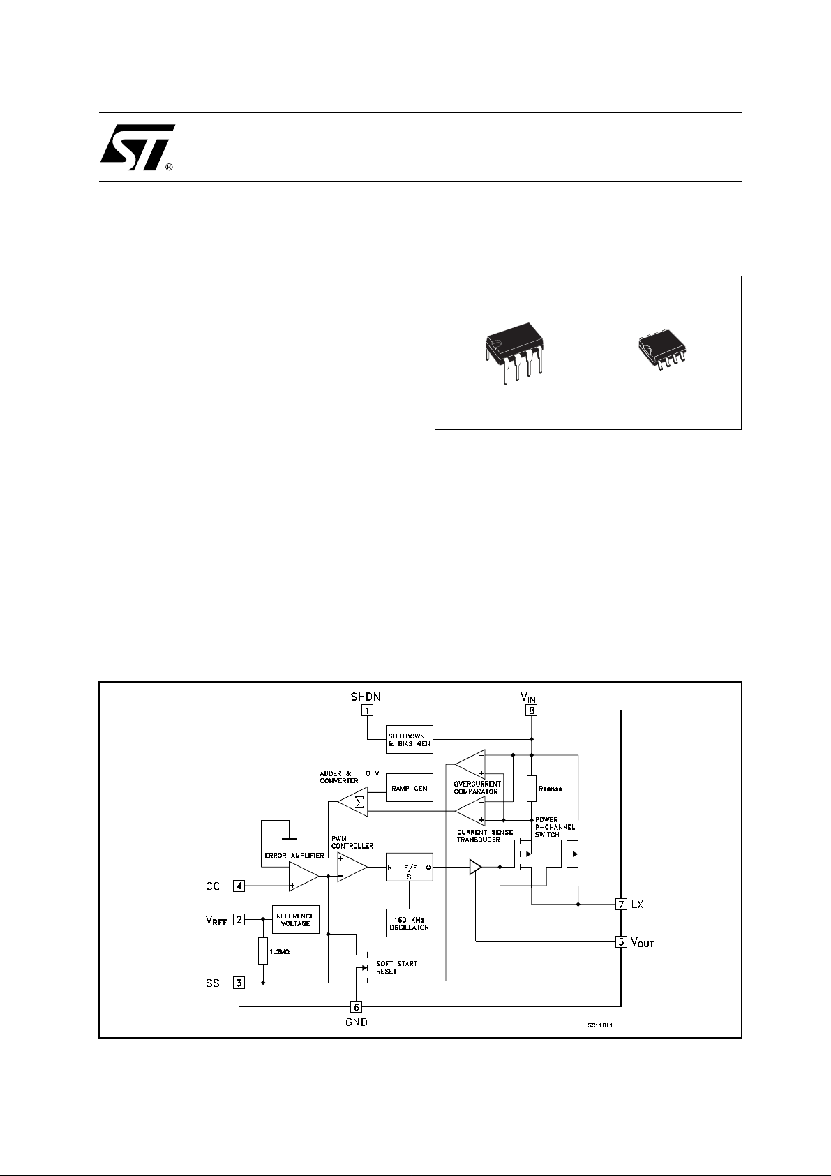
The ST735 is a Bi-CMOS, inverting s w itch mode
DC-DC regulator with internal Power MOSFE T's
that generates a fixed -5V output voltage from a
4V to 6.2V input voltage; is guaranteed an output
current of 200mA for inputs great er than 4.5V . The
quiescent current for this device is typically of
0.8mA and, in shutdown mode it is reduced to
10µA.
ST735
DIP-8 SO-8
These power-conserving features, along with hi gh
efficiency and applications circuits, t hat lend itself
to minaturization, make the ST735 excellent in a
broad range of on-card, HDD and portable
equipment applications. The ST735 employ a
high performance current mode puls e with
modulation (PWM) control scheme to provide tight
output voltage regulat ion and low noise. T he
fixed frequency oscillator is factory trimmed to
160KHz, allowing for easy noise filtering. T he
regulator in production is tested to guarantee an
output accuracy within ±5% over all specified
conditions.
SCHEMATIC DIAGRAM
1/9August 2002
ST735
ABSOLUTE MAXIMUM RATINGS
Symbol Parameter Value Unit
V
SHDN
V
V
V
OUT
I
LX
P
T
T
Absolute Maximum Ratings are those values beyond which damage to the device may occur. Functional operation under these condition is
not implied.
THERMAL DATA
Symbol Parameter DIP-8 SO-8 Unit
R
thj-case
DC Input Voltage (VINto GND)
IN
Shutdown Voltage (SHDN to GND) -0.3 to V
Switch Voltage (Lx to VIN)
LX
Feedback Voltage (V
FB
Output Voltage (V
OUT
to GND)
OUT
to GND)
Other Input Voltage (SS, CC to GND) -0.3 to V
Peack Switch Current
Power Dissipation at Tj= 70°C DIP-8 725
tot
Storage Temperature Range
stg
Operating Junction Temperature Range
op
Thermal Resistance Junction-case
SO-8 470
2 8 °C/W
-0.3 to +7 V
+0.3
+
V
-12.5 to +0.3 V
-11to+0.3 V
-11to+0.3 V
+0.3
+
V
2A
mW
-55 to +150 °C
-40 to +125 °C
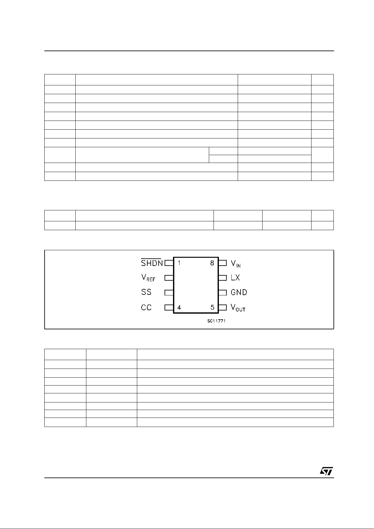
CONNECTION DIAGRAM (t op v iew)
PIN DESCRIPTION
Pin N° Symbol Name and Function
1 SHDN SHUT-DOWN Control (VCC=ON GND=Shutdown
2V
REF
3 SS Soft Start
4 CC Compensation Input
5V
OUT
6 GND Ground
7 LX Switch Output
8V
IN
Reference Output Voltage
Negative Output Voltage
Positive Supply - Voltage Input
2/9
ORDERING CODES
TYPE DIP-8 SO-8 SO-8 (T&R)
ST735 ST735CN ST735CD ST735CD-TR
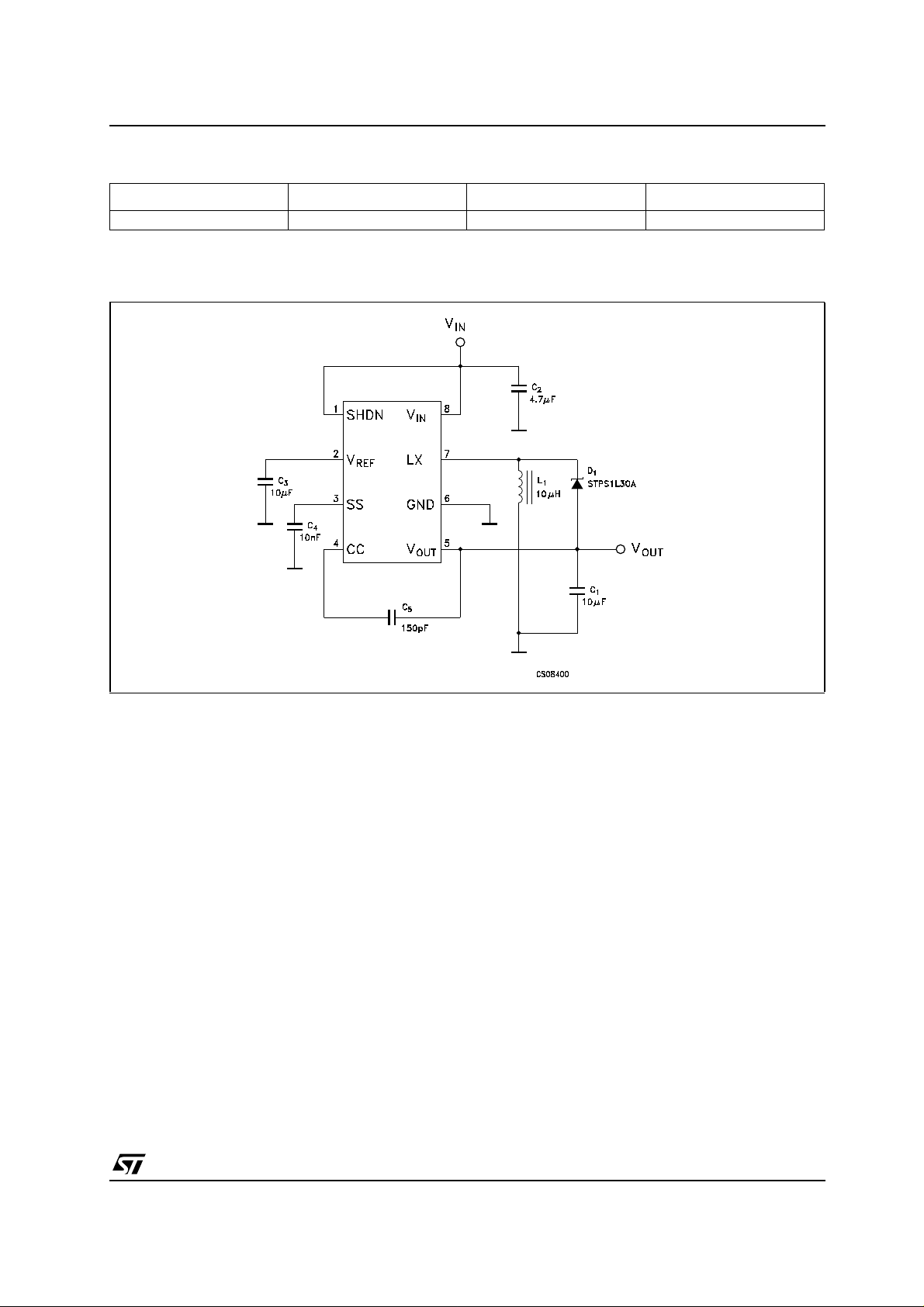
TYPICAL APPLICATION CIRCUIT
ST735
NOTE:
1) All capacitors are X7R ceramic
2) C
can be omitted if are used higher values for the input and output capacitors C2=47µF, C1=100pF.
5
3/9

ST735
ELECTRICAL CHARACTERISTICS (Refer to test circuit, VIN=5V,CIN=4.7µF, C
T
= -40 to 125°C, unless otherwise specified. Typical value are referred at T
amb
=10µF, L = 10µH,
OUT
= 25°C)
amb
Symbol Parameter Test Conditions Min. Typ. Max. Unit
V
V
I
I
SUPPLY
I
STANDBY
V
∆V
∆V
V
∆V
R
DSON
I
LEAK
V
f
R
Note1 : Tested at I
Input Voltage 4 6.2 V
IN
Output Voltage VIN= 4.5V to 6.2V I
OUT
T
amb
V
IN
T
amb
OUT
Output Current
V
V
T
V
IN
IN
amb
IN
= -40 to 125°C
= 4.0V to 6.2V I
= -40 to 125°C
= 4.5V to 6.2V T
= 4.5V to 6.2V I
= -40 to 125°C
= 4.0V V
OUT
= 0 to 200mA
OUT
= 0 to 175mA
OUT
= 0 to 125°C
amb
= 0 to 175mA
OUT
-5.25 -5 -4.75 V
-5.25 -5 -4.75 V
200 275 mA
175 mA
= -5V 175 mA
Supply Current Includes Switch Current 0.8 1.6 mA
Standby Current V
Short Circuit Current 1.5 A
I
SC
Undervoltage Lock-out 3.5 4 V
LO
Line Regulation VIN= 4.0V to 6.2V 0.1 %/V
OUT
Load Regulation I
OUT
Reference Voltage
REF
Reference Drift
REF
=0V 1 10 µA
SHDN
= 0 to 200mA 0.003 %/mA
OUT
T
=25°C (Note 1)
amb
T
= -40 to 125°C
amb
1.247 V
50 ppm/°C
LX ON Voltage 0.5 Ω
LX Leakage Current VDS= 10V 1 µA
Shutdown Pin Current 1 µA
I
SH
Shutdown Input Low
V
IL
Threshold
Shutdown Input High
IH
Threshold
Maximum Oscillator
OSC
Frequency
ν Efficency I
Compensation Pin
CC
Impedance on CC Pin
=0mA
VREF
= 100mA 72 %
OUT
2V
160 KHz
7.5 KΩ
0.25 V
4/9

ST735
TYPICAL CHARACTERISTICS
(Referredtotypicalapplicationcircuit,T
Figure1 : Output Voltage vs Temperature
Figure2 : Reference Voltage vs Temperatu re
=25°C unless otherwise specified)
amb
Figure4 : EfficencyvsTemperature
Figure5 : Efficency vs Ouput Current
Figure3 : Oscillator Frequency vs Temperature
Figure6 : Supply Currentvs Temperature
5/9

ST735
Figure7 : Supply Current vs Input Voltage
Figure8 : Shutdown Threshold vs Temp eratu re
Figure10 : Switch Current Limit vs Soft Start
Voltage
Figure11 : LX On Resistance vs Temperature
Figure9 : Peak Inductor Current vs Output
Current
6/9
Figure12 : LX On Resistance vs Input Voltage

Plastic DIP-8 MECHANICAL DATA
ST735
DIM.
MIN. TYP MAX. MIN. TYP. MAX.
A 3.3 0.130
a1 0.7 0.028
B 1.39 1.65 0.055 0.065
B1 0.91 1.04 0.036 0.041
b 0.5 0.020
b1 0.38 0.5 0.015 0.020
D 9.8 0.386
E 8.8 0.346
e 2.54 0.100
e3 7.62 0.300
e4 7.62 0.300
F 7.1 0.280
I 4.8 0.189
L 3.3 0.130
Z 0.44 1.6 0.017 0.063
mm. inch
P001F
7/9

ST735
SO-8 MECHANICAL DATA
DIM.
A 1.75 0.068
a1 0.1 0.25 0.003 0.009
a2 1.65 0.064
a3 0.65 0.85 0.025 0.033
b 0.35 0.48 0.013 0.018
b1 0.19 0.25 0.007 0.010
C 0.25 0.5 0.010 0.019
c1 45˚ (typ.)
D 4.8 5.0 0.189 0.196
E 5.8 6.2 0. 228 0.244
e 1.27 0.050
e3 3.81 0.150
F 3.8 4.0 0.149 0.157
L 0.4 1. 27 0. 015 0.050
M 0.6 0. 023
S
MIN. TYP MAX. MIN. TYP. MAX.
mm. inch
˚ (max.)
8
8/9
0016023

ST735
Information furnished is believed to be accurate and reliable. However, STMicroelectronics assumes no responsibi lity f or the
consequences of use of such informatio n nor for any infringement of paten ts or o ther rig hts of t hird part ies which ma y result from
its use. No license is granted by implication or otherwise under any patent or patent rights of STMicroelectronics. Specifications
mentioned in this publication are subject to change without notice. This publication supersedes and replaces all information
previousl y suppl ied. STM icroel ectronics produc ts are not auth orized for use as c ritica l compone nts in l ife s upport dev ices or
systems without express written approval of STMicroelectronics.
Australia - Brazil - Canada - China - Finland - France - Germany - Hong Kong - India - Israel - Italy - Japan - Malaysia - Malta - Morocco
© The ST logo is a registered trademark of STMicroelectronics
© 2002 STMicroelectronics - Printed in Italy - All Rights Reserved
STMicroelectronics GROUP OF COMPANIES
Singapore - Spain - Sweden - Switzerland - United Kingdom - United States.
© http://www.st.com
9/9
 Loading...