

Datasheet ST72T512R4, ST72T532R4, ST72T511R9, ST72T511R7, ST72T311R9 Datasheet (SGS Thomson Microelectronics)
...
Rev. 2.1
February 2000 1/164
ST72311R, ST72511R,
ST72512R, ST72532R
8-BIT MCU WITH NESTED INTERRUPTS, EEPROM, ADC,
16-BIT TIMERS, 8-BIT PWM ART, SPI, SCI, CAN INTERFACES
DATASHEET
■ Memories
– 16K to 60K bytes Program memory
(ROM,OTP and EPROM)
with read-out protection
– 256 bytes E2PROM Data memory
(only on ST72532R4)
– 1024 to 2048 bytes RAM
■ Clock, Reset and Supply Management
– Enhanced reset system
– Low voltage supply supervisor
– Clock sources: crystal/ceramic resonator os-
cillator or external clock
– Beep and Clock-out capability
– 4 Power Saving Modes: Halt, Active-Halt,
Wait and Slow
■ Interrupt Management
– Nested interrupt controller
– 13 interrupt vectors plus TRAP and RESET
– 15 external interrupt lines (on 4 vectors)
– TLI dedicated top level interrupt pin
■ 48 I/O Ports
– 48 multifunctional bidirectional I/O lines
– 32 alternate function lines
– 12 high sink outputs
■ 5 Timers
– Configurable watchdog timer
– Real time clock timer
– One 8-bit auto-reload timer with 4 independ-
ent PWM output channels, 2 input captures,
output compares and external clock with
event detector (except on ST725x2R4)
– Two 16-bittimerswith:2 input captures, 2out-
put compares,external clock input on one tim-
er, PWM and Pulse generator modes
■ 3 Communications Interfaces
– SPI synchronous serial interface
– SCI asynchronous serial interface
– CAN interface (except on ST72311Rx)
■ 1 Analog peripheral
– 8-bit ADC with 8 input channels
■ Instruction Set
– 8-bit data manipulation
– 63 basic instructions
– 17 main addressing modes
– 8 x 8 unsigned multiply instruction
– True bit manipulation
■ Development Tools
– Full hardware/software development package
Device Summary
Note 1. See Section 12.3.1 on page 133 for more information on VDDversus f
OSC
.
TQFP64
14 x 14
Features ST72511R9 ST72511R7 ST72511R6 ST72311R9 ST72311R7 ST72311R6 ST72512R4 ST72532R4
Program memory -bytes 60K 48K 32K 60K 48K 32K 16K 16K
RAM (stack) - bytes 2048 (256) 1536 (256) 1024 (256) 2048 (256) 1536 (256) 1024 (256) 1024 (256) 1024 (256)
EEPROM - bytes - - - ----256
Peripherals
watchdog, two 16-bit timers, 8-bit PWM
ART, SPI,SCI, CAN, ADC
watchdog, two 16-bit timers, 8-bit PWM
ART, SPI, SCI, ADC
watchdog, two 16-bit timers,
SPI, SCI, CAN, ADC
Operating Supply 3.0V to 5.5V 3.0 to 5.5V
1)
CPU Frequency 2 to 8 MHz (with 4 to 16 MHz oscillator) 2 to 4 MHz
1)
Operating Temperature -40°C to +85°C (-40°C to +105/125°C optional)
Packages TQFP64
1

Table of Contents
164
2/164
2
1 GENERAL DESCRIPTION . . . . . . ................................................ 6
1.1 INTRODUCTION . ....................................................... 6
1.2 PIN DESCRIPTION . . . . . . ................................................ 7
1.3 REGISTER & MEMORY MAP . . . . . . . . . . . . . . . .............................. 11
2 EPROM PROGRAM MEMORY . . . . . . . ........................................... 15
3 DATA EEPROM . . . . . . . . . .................................................... 16
3.1 INTRODUCTION . ...................................................... 16
3.2 MAIN FEATURES . . . . . . . . . . . . . . . . . . . . . . . . . . . . . . . . . . .................... 16
3.3 MEMORY ACCESS . . . . . . . . . . . . . . . . . . . . . . . . . . . . . . . . . . . . . . . . . . . . . ........ 17
3.4 POWER SAVING MODES . . . . . . ......................................... 18
3.5 ACCESS ERROR HANDLING . . . . . . . . . . . ................................. 18
3.6 REGISTER DESCRIPTION . . . . . . . . . . . . . . . . . . . . . . . . . . . . . . . . . . . . . . . ........ 19
4 CENTRAL PROCESSING UNIT . . ............................................... 20
4.1 INTRODUCTION . ...................................................... 20
4.2 MAIN FEATURES . . . . . . . . . . . . . . . . . . . . . . . . . . . . . . . . . . .................... 20
4.3 CPU REGISTERS . . . . . . . . . . . . . . . . . . . . . ................................. 20
5 SUPPLY, RESET AND CLOCK MANAGEMENT . . . . ................................23
5.1 LOW VOLTAGE DETECTOR (LVD) . . . . . . . . ................................24
5.2 RESET SEQUENCE MANAGER (RSM) . . . . . ................................25
5.2.1 Introduction . . . . . . . . . . . . ...........................................25
5.2.2 Asynchronous External RESET pin . . . .................................26
5.2.3 Internal Low Voltage Detection RESET . . . . . . . . . . . . . . . . . . . . . . ........... 26
5.2.4 Internal Watchdog RESET . . . ........................................ 26
5.3 LOW CONSUMPTION OSCILLATOR . . . . . .................................. 27
6 INTERRUPTS .. ............................................................. 28
6.1 INTRODUCTION . ...................................................... 28
6.2 MASKING AND PROCESSING FLOW . . . . . . . . . . . . . . . . . . . . . . . . . . . . . . . . . . . . . . 28
6.3 INTERRUPTS AND LOW POWER MODES . . . . . . . . . . . . . . . . . . . . . . . . . . . . . . . . . . 30
6.4 CONCURRENT & NESTED MANAGEMENT . . . . . . . . . . . . . .................... 30
6.5 INTERRUPT REGISTER DESCRIPTION . . . ................................. 31
7 POWER SAVING MODES . . . . . . . . . . ........................................... 34
7.1 INTRODUCTION . ...................................................... 34
7.2 SLOW MODE . . . . . . . . . . . . . . ...........................................34
7.3 WAIT MODE . . . . . . . . . . . ............................................... 35
7.4 ACTIVE-HALT AND HALT MODES . . . . . . . . . . . . . . . . . . . . . . . . . . . . . . . . . . . . . . . . 36
7.4.1 ACTIVE-HALT MODE . . . . . . . . . . . . . . . . . . . . . . . . . . . . . . . . . . . . . . . . . . . . . . . 36
7.4.2 HALT MODE . . . . . . . . . . . . . . . . . . . . . . . . . . . . . . . . . . . . . . . . . . . . . . . . . . . . . . 37
8 I/O PORTS . . . . . . . . . . . . . . . . . . . . . . . . . . ........................................ 38
8.1 INTRODUCTION . ...................................................... 38
8.2 FUNCTIONAL DESCRIPTION . . . . ........................................38
8.2.1 Input Modes . . .................................................... 38
8.2.2 Output Modes . . . . . . . . . . . . . ........................................38
8.2.3 Alternate Functions . . . . . . ...........................................38

Table of Contents
3/164
3
8.3 I/O PORT IMPLEMENTATION . . . . ........................................41
8.4 LOW POWER MODES . . . . . . . . . . . . . . . . . ................................. 42
8.5 INTERRUPTS . . . . . . . . . . . . . . . . . . . . . . . . ................................. 42
8.5.1 Register Description . . . . . ........................................... 43
9 MISCELLANEOUS REGISTERS . . . . . . . . . . . . . . .................................. 45
9.1 I/O PORT INTERRUPT SENSITIVITY .. . . . . ................................45
9.2 I/O PORT ALTERNATE FUNCTIONS . . . . . ..................................45
9.3 MISCELLANEOUS REGISTERS . . . . . . . . . . . . . . . . . . . . . . . . . . . . . . . . . . . . . . . . . . 46
10 ON-CHIPPERIPHERALS . . . . . . ............................................... 49
10.1 WATCHDOG TIMER (WDG) . . . . . . . . . . . . . . . . . . . ........................... 49
10.1.1 Introduction . . . . . . . . . . . . . . . ........................................ 49
10.1.2 Main Features . . . . . . . . . . . . . . . . . . . . . . . . . . . . . . . . . . . . . . . . . . . . . ........ 49
10.1.3 Functional Description . . . . . . . . . . . . . . . . . . . . . . . . . . . . . . . . . . . . . . . . . . . . . . 49
10.1.4 Hardware Watchdog Option . . ........................................50
10.1.5 Low Power Modes .. ............................................... 50
10.1.6 Interrupts . . ....................................................... 50
10.1.7 Register Description . ............................................... 50
10.2 MAIN CLOCK CONTROLLER WITH REAL TIME CLOCK TIMER (MCC/RTC) . . . . . . . 52
10.2.1 Programmable CPU Clock Prescaler . . . . . . . . . . . . . . . . . . . . ............... 52
10.2.2 Clock-out Capability . . . . . . . . . . . . . . . . . . . . . . . . . . . . . . . . . . . . . . . . . . . . . . . . 52
10.2.3 Real Time Clock Timer (RTC) ........................................ 52
10.2.4 Register Description . ............................................... 53
10.2.5 Low Power Modes . . . . . . . . . ........................................53
10.2.6 Interrupts . . ....................................................... 53
10.3 PWM AUTO-RELOAD TIMER (ART) . . . . . . . ................................54
10.3.1 Introduction . . . . . . . . . . . . . . . ........................................ 54
10.3.2 Functional Description . . . . . . . . . . . . . . . . . . . . . . . . . . . . . . . . . . . . . . . . . . . . . . 55
10.3.3 Register Description . ............................................... 58
10.4 16-BIT TIMER . . . . . . . . . . . . . . . . . . . . . . . . . . . . . . . . . . . . . . . . . . . . . . . . . ........ 61
10.4.1 Introduction . . . . . . . . . . . . . . . ........................................ 61
10.4.2 Main Features . . . . . . . . . . . . . . . . . . . . . . . . . . . . . . . . . . . . . . . . . . . . . ........ 61
10.4.3 Functional Description . . . . . . . . . . . . . . . . . . . . . . . . . . . . . . . . . . . . . . . . . . . . . . 61
10.4.4 Low Power Modes . . . . . . . . . ........................................73
10.4.5 Interrupts . . . . . . . . . . . . . ...........................................73
10.4.6 Summary of Timer modes . . . . . . . . . . .................................73
10.4.7 Register Description . ............................................... 74
10.5 SERIAL PERIPHERAL INTERFACE (SPI) . .................................. 79
10.5.1 Introduction . . . . . . . . . . . . . . . ........................................ 79
10.5.2 Main Features . . . . . . . . . . . . . . . . . . . . . . . . . . . . . . . . . . . . . . . . . . . . . ........ 79
10.5.3 Generaldescription . . . . . . . . . ........................................ 79
10.5.4 Functional Description . . . . . . . . . . . . . . . . . . . . . . . . . . . . . . . . . . . . . . . . . . . . . . 81
10.5.5 Low Power Modes .. ............................................... 88
10.5.6 Interrupts . . . . . . . . . . . . . ...........................................88
10.5.7 Register Description . ............................................... 89

ST72311R, ST72511R, ST72512R, ST72532R
4/164
10.6 SERIAL COMMUNICATIONS INTERFACE (SCI) . . . . . . . . . . . . . . . . . . . . . . . . . . . . . . 92
10.6.1 Introduction . . . . . . . . . . . . . . . ........................................ 92
10.6.2 Main Features . . . . . . . . . . . . . . . . . . . . . . . . . . . . . . . . . . . . . . . . . . . . . ........ 92
10.6.3 GeneralDescription . . . . . . . . . . . . . . . . . . . . . . . . . . . . .................... 92
10.6.4 Functional Description . . . . . . . . . . . . . . . . . . . . . . . . . . . . . . . . . . . . . . . . . . . . . . 94
10.6.5 Low Power Modes .. ............................................... 99
10.6.6 Interrupts . . ....................................................... 99
10.6.7 Register Description . ..............................................100
10.7 CONTROLLER AREA NETWORK (CAN) . . . ................................ 104
10.7.1 Introduction . . . . . . . . . . . . . . . ....................................... 104
10.7.2 Main Features . . . . . . . . . . . . . . . . . . . . . . . . . . . . . . . . . . . . . . . . . . . . . ....... 105
10.7.3 Functional Description . . . . . . . . . . . . . . . . . . . . . . . . . . . . . . . . . . . . . . . . . . . . . 105
10.7.4 Register Description . ..............................................111
10.8 8-BIT A/D CONVERTER (ADC) .......................................... 121
10.8.1 Introduction . . . . . . . . . . . . . . . ....................................... 121
10.8.2 Main Features . . . . . . . . . . . . . . . . . . . . . . . . . . . . . . . . . . . . . . . . . . . . . ....... 121
10.8.3 Functional Description . . . . . . . . . . . . . . . . . . . . . . . . . . . . . . . . . . . . . . . . . . . . . 121
10.8.4 Low Power Modes . . . . . . . . . .......................................122
10.8.5 Interrupts . . ...................................................... 122
10.8.6 Register Description . ..............................................123
11 INSTRUCTION SET . . . . . . . . . . . . . . . . . . . . . . . . ................................ 125
11.1 ST7 ADDRESSING MODES . . . . . . . . . . . . . . . . . . . . . . . . . . . . . . . . . . . . . . . . . . . . . 125
11.1.1 Inherent.........................................................126
11.1.2 Immediate . . ..................................................... 126
11.1.3 Direct . . . . . . . . . . . . . . . . .......................................... 126
11.1.4 Indexed(No Offset, Short, Long) . . . . . . ............................... 126
11.1.5 Indirect (Short, Long) . . . . . . . . . . . . . . . . . . . . .......................... 126
11.1.6 Indirect Indexed (Short, Long) .......................................127
11.1.7 Relative mode (Direct, Indirect) . . . . . . ................................ 127
11.2 INSTRUCTION GROUPS . . . . . . . . . . . . . . . . . . ............................. 128
12 ELECTRICAL CHARACTERISTICS . . . . ........................................ 131
12.1 PARAMETER CONDITIONS . . . . . . . . . . . . . . . . .............................131
12.1.1 Minimum and Maximum values . . . . . . . . . . . . . . . . . . . . . . . . . . . . . . . . . . . . . . 131
12.1.2 Typical values . . . . . . . . . . . . . . . . . . . . . ...............................131
12.1.3 Typical curves . . . . . . . . . . . . . ....................................... 131
12.1.4 Loading capacitor . . . . . . . . . . .......................................131
12.1.5 Pin input voltage . . . . . . . . . . . . . . . . . . . . . . . . . . . . . . . . . . . . . . . . . . . . . . . . . . 131
12.2 ABSOLUTE MAXIMUM RATINGS . . . . . . . . . . . . . . . . . . . . . . . . . . . . . . . . . . . . . . . . 132
12.2.1 Voltage Characteristics . . . . . . . . . . . . ................................ 132
12.2.2 Current Characteristics . . . . . . . . . . . . . . . . . . . . . . . . . . . . . . . . . . . . . . . . . . . . 132
12.2.3 Thermal Characteristics . . . . . . . . . . . . . . . ............................. 132
12.3 OPERATING CONDITIONS . . . . . . . . . . ................................... 133
12.3.1 GeneralOperating Conditions . . . . . . . . . . . . . . . . . . . . . . . . . . . . . . . . ....... 133
12.3.2 OperatingConditions with Low Voltage Detector (LVD) . . . . . . . . . . . . . ....... 134
12.4 SUPPLY CURRENT CHARACTERISTICS . . . ...............................135
12.4.1 RUN and SLOW Modes . . . . . . . . . . . . . . . . . . . . . . . . . ................... 135
12.4.2 WAIT and SLOW WAIT Modes .. . . . ................................. 136

ST72311R, ST72511R, ST72512R, ST72532R
5/164
12.4.3 HALT and ACTIVE-HALT Modes . . . . . ...............................137
12.4.4 Supply and Clock Managers . . . . . . ................................... 137
12.4.5 On-ChipPeripheral . . . . . . . . . . . . . . . . . . . . . . . . . . . . . . . . . . . . . . . . . . . . . . . 137
12.5 CLOCK AND TIMING CHARACTERISTICS . . . . . . . . . . . . . . . . . . . . . . . ..........138
12.5.1 GeneralTimings . . . .............................................. 138
12.5.2 External Clock Source .. . . . . . . . . . . . . . . . . . . . . . . . . . . . . . . . . . . . . . . . . . . . 138
12.5.3 Crystal and Ceramic Resonator Oscillators . . . . . . . . . . . . . . . . . . . . . . . . . . . . . 138
12.6 MEMORY CHARACTERISTICS . . . .......................................139
12.6.1 RAM and Hardware Registers . . . . . . . ................................ 139
12.6.2 EEPROM Data Memory . . . . . . . . . . . . . . . . . . . . . . . . . . . . . . . . . . . . . . . . . . . . 139
12.6.3 EPROM Program Memory . . . .......................................139
12.7 EMC CHARACTERISTICS . . . . . . . . . . . . . . . . . . . . . . . . . . . . . . . . . . . . . . . . . . . . . . 140
12.7.1 Functional EMS . . . . . . . . . . . . . . . . . . ................................ 140
12.7.2 Absolute Electrical Sensitivity . .......................................141
12.7.3 ESD Pin Protection Strategy . . . . . . . . . ................................ 143
12.8 I/O PORT PIN CHARACTERISTICS .......................................145
12.8.1 GeneralCharacteristics .. . . . .......................................145
12.8.2 OutputDriving Current . . . . . . .......................................146
12.9 CONTROL PIN CHARACTERISTICS . . . . . ................................. 147
12.9.1 Asynchronous RESET Pin .......................................... 147
12.9.2 VPP Pin . . . . . . . . . . . . . . . . . . . . . . . . . ...............................147
12.10 TIMER PERIPHERAL CHARACTERISTICS . . . . . . . . . . . . . . . . . . . . . . . . . . ....... 148
12.10.1Watchdog Timer . . . . . . . . . . . . . . . . . . . . . . . . . . . . . . . . . . . . . . . . . . ....... 148
12.10.28-Bit PWM-ART Auto-Reload Timer . ................................. 148
12.10.316-Bit Timer . . . . . . . . . . . . . . . . . . . . . ................................ 148
12.11 COMMUNICATIONS INTERFACE CHARACTERISTICS . . . . . . . . . . . . . . . . . . . . . . . 149
12.11.1SPI - Serial Peripheral Interface . . . . . . . . . . . . .......................... 149
12.11.2SCI - Serial Communications Interface . . . . . . . . . . . . . . . . . . . . . . ..........151
12.11.3CAN - Controller Area Network Interface . . . . . . . . . . . . ................... 151
12.12 8-BIT ADC CHARACTERISTICS .. . . . . . . ................................. 152
13 PACKAGE CHARACTERISTICS . . . . . . ........................................ 154
13.1 PACKAGE MECHANICAL DATA . . . . . . . . . . . . ............................. 154
13.2 THERMAL CHARACTERISTICS . . . . . . . . . . . ...............................155
13.3 SOLDERING AND GLUEABILITY INFORMATION . . . . . . . . . . . . . . . . . . . . . ....... 156
13.4 PACKAGE/SOCKET FOOTPRINT PROPOSAL . . . . . . . . . . . ................... 157
14 DEVICE CONFIGURATION AND ORDERING INFORMATION . . . . . . . . . . . . . . . . . . . . . . . 158
14.1 OPTION BYTES . . . ...................................................158
14.2 DEVICE ORDERING INFORMATION AND TRANSFER OF CUSTOMER CODE . . . . 159
14.3 DEVELOPMENT TOOLS . . . . . . . . . . . . . . . . . . . . . .......................... 161
15 ST7 GENERIC APPLICATION NOTE . . . ....................................... 162
16 SUMMARY OF CHANGES . ..................................................163
ST72311R, ST72511R, ST72512R, ST72532R
6/164
1 GENERAL DESCRIPTION
1.1 INTRODUCTION
The ST72311R, ST72511R, ST72512R and
ST72532R devices are members of the ST7 microcontroller family. They can be grouped as follows:
– ST725xxR devices are designed for mid-range
applications witha CAN bus interface(Controller
Area Network)
– ST72311R devices target the same range of ap-
plications but without CAN interface.
All devices are based on a common industrystandard 8-bit core, featuringan enhancedinstruction set.
Under software control, all devices can be placed
in WAIT, SLOW, ACTIVE-HALT or HALT mode,
reducing power consumption when the application
is in idle or standby state.
The enhanced instruction set and addressing
modes of the ST7 offer both power and flexibility to
software developers, enabling the design of highly
efficient and compact application code. In addition
to standard 8-bit data management, allST7 microcontrollers feature true bit manipulation, 8x8 unsigned multiplication and indirect addressing
modes.
Figure 1. Device Block Diagram
8-BIT CORE
ALU
ADDRESS AND DATA BUS
OSC1
V
PP
CONTROL
PROGRAM
(16K - 60K Bytes)
V
SS
RESET
PORT F
PF7:0
(8-BIT)
TIMER A
BEEP
PORT A
RAM
(1024, 2048 Bytes)
PORT C
8-BIT ADC
V
DDA
V
SSA
PORT B
PB7:0
(8-BIT)
PWM ART
PORT E
CAN
PE7:0
(8-BIT)
SCI
TIMER B
PA7:0
(8-BIT)
PORT D
PD7:0
(8-BIT)
SPI
PC7:0
(8-BIT)
V
DD
EEPROM
(256 Bytes)
WATCHDOG
TLI
OSC
LVD
OSC2
MEMORY
MCC/RTC
4
ST72311R, ST72511R, ST72512R, ST72532R
7/164
1.2 PIN DESCRIPTION
Figure 2. 64-Pin TQFP Package Pinout
V
DDA
V
SSA
V
DD_3
V
SS_3
MCO / PF0
BEEP / PF1
PF2
OCMP2_A / PF3
OCMP1_A / PF4
ICAP2_A / PF5
ICAP1_A / (HS) PF6
EXTCLK_A / (HS) PF7
AIN4 / PD4
AIN5 / PD5
AIN6 / PD6
AIN7 / PD7
64 63 62 61 60 59 58 57 56 55 54 53 52 51 50 49
48
47
46
45
44
43
42
41
40
39
38
37
36
35
34
33
17 18 19 20 21 22 23 24 29 30 31 3225 26 27 28
1
2
3
4
5
6
7
8
9
10
11
12
13
14
15
16
ei2
ei3
ei0
ei1
PWM3 / PB0
PWM2 / PB1
PWM1 / PB2
PWM0 / PB3
ARTCLK / PB4
PB5
PB6
PB7
AIN0 / PD0
AIN1 / PD1
AIN2 / PD2
AIN3 / PD3
(HS) PE4
(HS) PE5
(HS) PE6
(HS) PE7
PA1
PA0
PC7 / SS
PC6 / SCK
PC5 / MOSI
PC4 / MISO
PC3 (HS) / ICAP1_B
PC2 (HS) / ICAP2_B
PC1 / OCMP1_B
PC0 / OCMP2_B
V
SS_0
V
DD_0
V
SS_1
V
DD_1
PA3
PA2
V
DD
_2
OSC1
OSC2
V
SS
_2
TLIncRESET
V
PP
PA7 (HS)
PA6 (HS)
PA5 (HS)
PA4 (HS)
PE3 / CANRX
PE2 / CANTX
PE1 / RDI
PE0 / TDO
(HS) 20mA high sink capability
eix associated external interrupt vector
5
ST72311R, ST72511R, ST72512R, ST72532R
8/164
PIN DESCRIPTION (Cont’d)
For external pin connection guidelines, refer to Section 12 ”ELECTRICAL CHARACTERISTICS” on page
131.
Legend / Abbreviations for Table 1:
Type: I = input, O = output, S = supply
Input level: A = Dedicated analog input
In/Output level: C = CMOS 0.3VDD/0.7VDD,
CT= CMOS 0.3VDD/0.7VDDwith input trigger
Output level: HS = 20mA high sink (on N-buffer only)
Port and control configuration:
– Input: float = floating, wpu = weak pull-up, int = interrupt1), ana = analog
– Output: OD = open drain2), PP = push-pull
Refer to Section 8 ”I/O PORTS” onpage 38 for more details on the software configuration of the I/O ports.
The RESET configuration of each pin is shown in bold. This configuration is valid as long as the device is
in reset state.
Table 1. Device Pin Description
Pin n°
Pin Name
Type
Level Port
Main
function
(after
reset)
Alternate function
TQFP64
Input
Output
Input Output
float
wpu
int
ana
OD
PP
1 PE4 (HS) I/O CTHS X X X X Port E4
2 PE5 (HS) I/O C
T
HS X X X X Port E5
3 PE6 (HS) I/O C
T
HS X X X X Port E6
4 PE7 (HS) I/O C
T
HS X X X X Port E7
5 PB0/PWM3 I/O C
T
X ei2 X X Port B0 PWM Output 3
6 PB1/PWM2 I/O C
T
X ei2 X X Port B1 PWM Output 2
7 PB2/PWM1 I/O C
T
X ei2 X X Port B2 PWM Output 1
8 PB3/PWM0 I/O C
T
X ei2 X X Port B3 PWM Output 0
9 PB4/ARTCLK I/O C
T
X ei3 X X Port B4 PWM-ART External Clock
10 PB5 I/O C
T
X ei3 X X Port B5
11 PB6 I/O C
T
X ei3 X X Port B6
12 PB7 I/O C
T
X ei3 X X Port B7
13 PD0/AIN0 I/O C
T
X X X X X Port D0 ADC Analog Input 0
14 PD1/AIN1 I/O C
T
X X X X X Port D1 ADC Analog Input 1
15 PD2/AIN2 I/O C
T
X X X X X Port D2 ADC Analog Input 2
16 PD3/AIN3 I/O C
T
X X X X X Port D3 ADC Analog Input 3
17 PD4/AIN4 I/O C
T
X X X X X Port D4 ADC Analog Input 4
18 PD5/AIN5 I/O C
T
X X X X X Port D5 ADC Analog Input 5
19 PD6/AIN6 I/O C
T
X X X X X Port D6 ADC Analog Input 6
20 PD7/AIN7 I/O C
T
X X X X X Port D7 ADC Analog Input 7
21 V
DDA
S Analog Power Supply Voltage
22 V
SSA
S Analog Ground Voltage
23 V
DD_3
S Digital Main Supply Voltage
6
ST72311R, ST72511R, ST72512R, ST72532R
9/164
24 V
SS_3
S Digital Ground Voltage
25 PF0/MCO I/O C
T
X ei1 X X Port F0 Main clock output (f
OSC
/2)
26 PF1/BEEP I/O C
T
X ei1 X X Port F1 Beep signal output
27 PF2 I/O C
T
X ei1 X X Port F2
28 PF3/OCMP2_A I/O C
T
X X X X Port F3 Timer A Output Compare 2
29 PF4/OCMP1_A I/O C
T
X X X X Port F4 Timer A Output Compare 1
30 PF5/ICAP2_A I/O C
T
X X X X Port F5 Timer A Input Capture 2
31 PF6 (HS)/ICAP1_A I/O C
T
HS X X X X Port F6 Timer A Input Capture 1
32 PF7 (HS)/EXTCLK_A I/O C
T
HS X X X X Port F7 Timer A External Clock Source
33 V
DD_0
S Digital Main Supply Voltage
34 V
SS_0
S Digital Ground Voltage
35 PC0/OCMP2_B I/O C
T
X X X X Port C0 Timer B Output Compare 2
36 PC1/OCMP1_B I/O C
T
X X X X Port C1 Timer B Output Compare 1
37 PC2 (HS)/ICAP2_B I/O C
T
HS X X X X Port C2 Timer B Input Capture 2
38 PC3 (HS)/ICAP1_B I/O C
T
HS X X X X Port C3 Timer B Input Capture 1
39 PC4/MISO I/O C
T
X X X X Port C4 SPI Master In / Slave Out Data
40 PC5/MOSI I/O C
T
X X X X Port C5 SPI Master Out / Slave In Data
41 PC6/SCK I/O C
T
X X X X Port C6 SPI Serial Clock
42 PC7/SS I/O C
T
X X X X Port C7 SPI Slave Select (active low)
43 PA0 I/O C
T
X ei0 X X Port A0
44 PA1 I/O C
T
X ei0 X X Port A1
45 PA2 I/O C
T
X ei0 X X Port A2
46 PA3 I/O C
T
X ei0 X X Port A3
47 V
DD_1
S Digital Main Supply Voltage
48 V
SS_1
S Digital Ground Voltage
49 PA4 (HS) I/O C
T
HS X X X X Port A4
50 PA5 (HS) I/O C
T
HS X X X X Port A5
51 PA6 (HS) I/O C
T
HS X T Port A6
52 PA7 (HS) I/O C
T
HS X T Port A7
53 V
PP
I
Must betied low in user mode. In programming
mode when available, this pin acts as the programming voltage input V
PP
.
54 RESET I/O C X X Top priority nonmaskable interrupt (active low)
55 NC Not Connected
56 NMI I C
T
X Non maskable interrupt input pin
57 V
SS_3
S Digital Ground Voltage
58 OSC2
3)
I/O
External clock mode input pull-up orcrystal/ceramic resonator oscillator inverter output
59 OSC1
3)
I
External clock input or crystal/ceramic resonator oscillator inverter input
60 V
DD_3
S Digital Main Supply Voltage
Pin n°
Pin Name
Type
Level Port
Main
function
(after
reset)
Alternate function
TQFP64
Input
Output
Input Output
float
wpu
int
ana
OD
PP

ST72311R, ST72511R, ST72512R, ST72532R
10/164
Notes:
1. In the interrupt input column, “eiX” defines the associated external interrupt vector. If the weak pull-up
column (wpu) is merged with the interrupt column (int), then the I/O configuration is pull-up interrupt input,
else the configuration is floating interrupt input.
2. In the open drain output column, “T” defines a true open drain I/O (P-Buffer and protection diode to V
DD
are not implemented). See Section 8 ”I/O PORTS” on page 38 and Section 12.8 ”I/O PORT PIN CHARACTERISTICS” on page 145 for more details.
3. OSC1and OSC2 pins connect acrystal/ceramic resonatoror an external sourceto theon-chip oscillator
see Section 1.2 ”PIN DESCRIPTION” on page 7 and Section 12.5 ”CLOCK AND TIMING CHARACTERISTICS” on page 138 for more details.
61 PE0/TDO I/O C
T
X X X X Port E0 SCI Transmit Data Out
62 PE1/RDI I/O C
T
X X X X Port E1 SCI Receive Data In
63 PE2/CANTX I/O C
T
X Port E2 CAN Transmit Data Output
64 PE3/CANRX I/O C
T
X X X X Port E3 CAN Receive Data Input
Pin n°
Pin Name
Type
Level Port
Main
function
(after
reset)
Alternate function
TQFP64
Input
Output
Input Output
float
wpu
int
ana
OD
PP
ST72311R, ST72511R, ST72512R, ST72532R
11/164
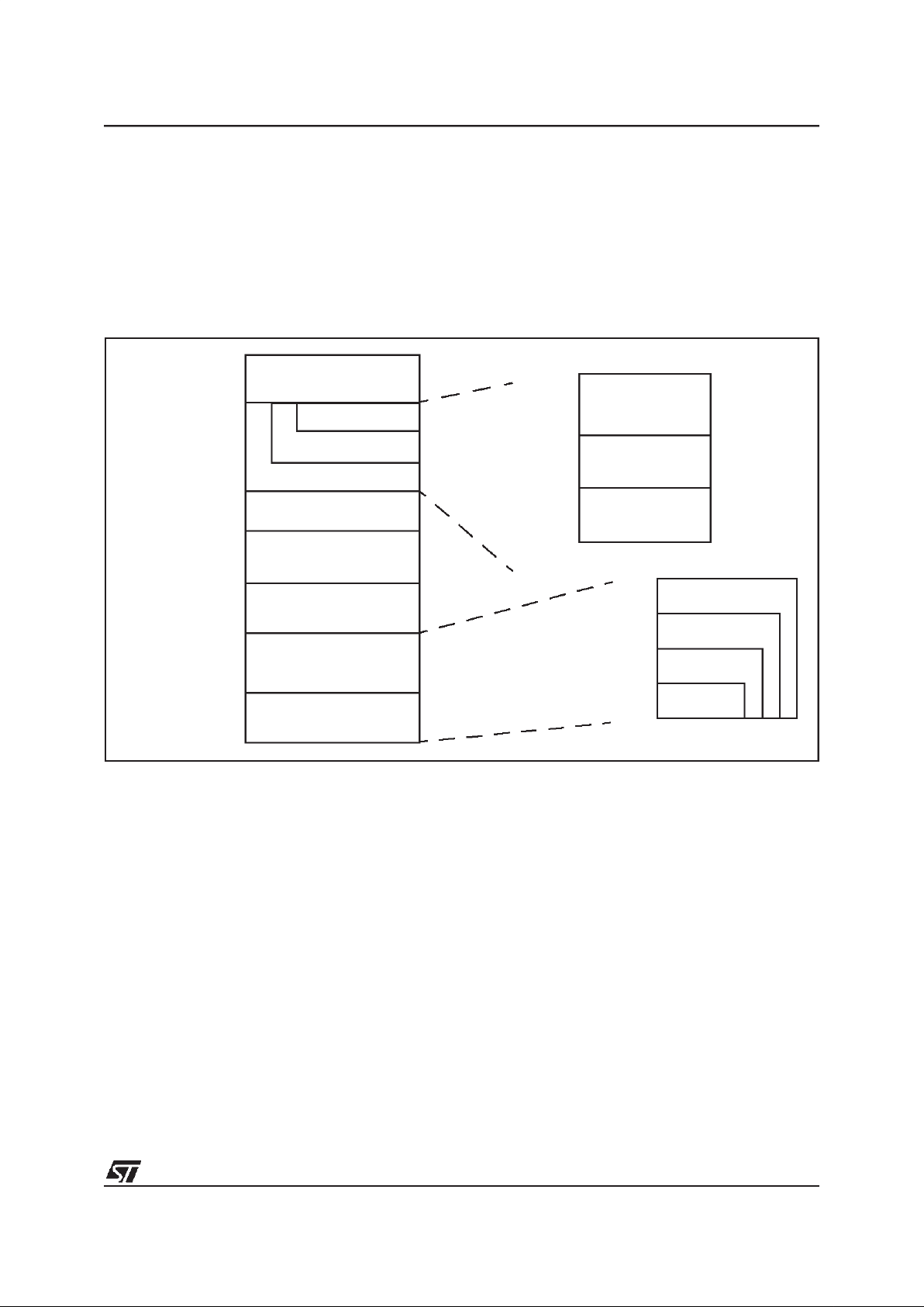
1.3 REGISTER & MEMORY MAP
As shown in the Figure 3, the MCU is capable of
addressing 64K bytes of memories and I/O registers.
The available memory locations consist of 128
bytes of register location, up to 2Kbytes of RAM,
up to 256 bytes of data EEPROM and up to
60Kbytes of user program memory. The RAM
space includes up to 256 bytes for the stack from
0100h to 01FFh.
The highest address bytes contain the user reset
and interrupt vectors.
Figure 3. Memory Map
0000h
1024 Bytes RAM
Program Memory
(60K, 48K, 32K, 16K Bytes)
Interrupt & Reset Vectors
HW Registers
0BFFh
0080h
007Fh
0D00h
0FFFh
Reserved
2048 Bytes RAM
(see Table 2)
1000h
FFDFh
FFE0h
FFFFh
(see Table 7 on page 32)
0C00h
0CFFh
Optional EEPROM
(256 Bytes)
0880h
Reserved
087Fh
Short Addressing
RAM (zero page)
Stack
(256 Bytes)
16-bit Addressing
RAM
0100h
01FFh
047Fh
0080h
0200h
00FFh
or 067Fh
or 087Fh
1536 Bytes RAM
16 KBytes
4000h
1000h
48 KBytes
C000h
8000h
32 KBytes
60 KBytes
FFFFh

ST72311R, ST72511R, ST72512R, ST72532R
12/164
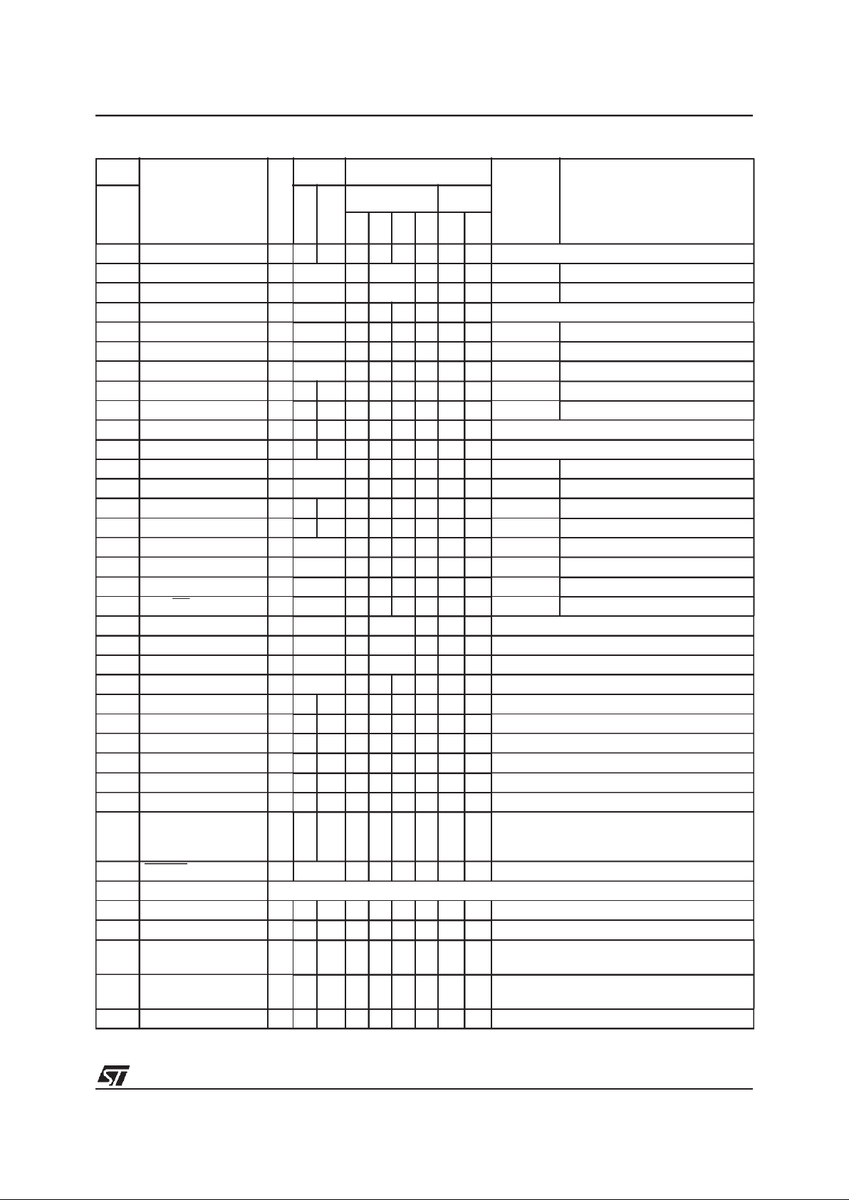
Table 2. Hardware Register Map
Address Block
Register
Label
Register Name
Reset
Status
Remarks
0000h
0001h
0002h
Port A
PADR
PADDR
PAOR
Port A Data Register
Port A Data Direction Register
Port A Option Register
00h
1)
00h
00h
R/W
R/W
R/W
2)
0003h Reserved Area (1 Byte)
0004h
0005h
0006h
Port C
PCDR
PCDDR
PCOR
Port C Data Register
Port C Data Direction Register
Port C Option Register
00h
1)
00h
00h
R/W
R/W
R/W
0007h Reserved Area (1 Byte)
0008h
0009h
000Ah
Port B
PBDR
PBDDR
PBOR
Port B Data Register
Port B Data Direction Register
Port B Option Register
00h
1)
00h
00h
R/W
R/W
R/W
000Bh Reserved Area (1 Byte)
000Ch
000Dh
000Eh
Port E
PEDR
PEDDR
PEOR
Port E Data Register
Port E Data Direction Register
Port E Option Register
00h
1)
00h
00h
R/W
R/W
2)
R/W
2)
000Fh Reserved Area (1 Byte)
0010h
0011h
0012h
Port D
PDDR
PDDDR
PDOR
Port D Data Register
Port D Data Direction Register
Port D Option Register
00h
1)
00h
00h
R/W
R/W
R/W
0013h Reserved Area (1 Byte)
0014h
0015h
0016h
Port F
PFDR
PFDDR
PFOR
Port F Data Register
Port F Data Direction Register
Port F Option Register
00h
1)
00h
00h
R/W
R/W
R/W
0017h
to
001Fh
Reserved Area (9 Bytes)
0020h MISCR1 Miscellaneous Register 1 00h R/W
0021h
0022h
0023h
SPI
SPIDR
SPICR
SPISR
SPI Data I/O Register
SPI Control Register
SPI Status Register
xxh
0xh
00h
R/W
R/W
Read Only
0024h
0025h
0026h
0027h
ITC
ISPR0
ISPR1
ISPR2
ISPR3
Interrupt Software Priority Register 0
Interrupt Software Priority Register 1
Interrupt Software Priority Register 2
Interrupt Software Priority Register 3
FFh
FFh
FFh
FFh
R/W
R/W
R/W
R/W
0028h Reserved Area (1 Byte)
0029h MCC MCCSR Main Clock Control / Status Register 01h R/W

ST72311R, ST72511R, ST72512R, ST72532R
13/164
002Ah
002Bh
WATCHDOG
WDGCR
WDGSR
Watchdog Control Register
Watchdog Status Register
7Fh
000x 000x
R/W
R/W
002Ch EEPROM EECSR Data EEPROM Control/Status Register 00h R/W
002Dh
to
0030h
Reserved Area (4 Bytes)
0031h
0032h
0033h
0034h
0035h
0036h
0037h
0038h
0039h
003Ah
003Bh
003Ch
003Dh
003Eh
003Fh
TIMER A
TACR2
TACR1
TASR
TAIC1HR
TAIC1LR
TAOC1HR
TAOC1LR
TACHR
TACLR
TAACHR
TAACLR
TAIC2HR
TAIC2LR
TAOC2HR
TAOC2LR
Timer A Control Register 2
Timer A Control Register 1
Timer A Status Register
Timer A Input Capture 1 High Register
Timer A Input Capture 1 Low Register
Timer A Output Compare 1 High Register
Timer A Output Compare 1 Low Register
Timer A Counter High Register
Timer A Counter Low Register
Timer A Alternate Counter High Register
Timer A Alternate Counter Low Register
Timer A Input Capture 2 High Register
Timer A Input Capture 2 Low Register
Timer A Output Compare 2 High Register
Timer A Output Compare 2 Low Register
00h
00h
xxh
xxh
xxh
80h
00h
FFh
FCh
FFh
FCh
xxh
xxh
80h
00h
R/W
R/W
Read Only
Read Only
Read Only
R/W
R/W
Read Only
Read Only
Read Only
Read Only
Read Only
Read Only
R/W
R/W
0040h MISCR2 Miscellaneous Register 2 00h R/W
0041h
0042h
0043h
0044h
0045h
0046h
0047h
0048h
0049h
004Ah
004Bh
004Ch
004Dh
004Eh
004Fh
TIMER B
TBCR2
TBCR1
TBSR
TBIC1HR
TBIC1LR
TBOC1HR
TBOC1LR
TBCHR
TBCLR
TBACHR
TBACLR
TBIC2HR
TBIC2LR
TBOC2HR
TBOC2LR
Timer B Control Register 2
Timer B Control Register 1
Timer B Status Register
Timer B Input Capture 1 High Register
Timer B Input Capture 1 Low Register
Timer B Output Compare 1 High Register
Timer B Output Compare 1 Low Register
Timer B Counter High Register
Timer B Counter Low Register
Timer B Alternate Counter High Register
Timer B Alternate Counter Low Register
Timer B Input Capture 2 High Register
Timer B Input Capture 2 Low Register
Timer B Output Compare 2 High Register
Timer B Output Compare 2 Low Register
00h
00h
xxh
xxh
xxh
80h
00h
FFh
FCh
FFh
FCh
xxh
xxh
80h
00h
R/W
R/W
Read Only
Read Only
Read Only
R/W
R/W
Read Only
Read Only
Read Only
Read Only
Read Only
Read Only
R/W
R/W
0050h
0051h
0052h
0053h
0054h
0055h
0056h
0057h
SCI
SCISR
SCIDR
SCIBRR
SCICR1
SCICR2
SCIERPR
SCIETPR
SCI Status Register
SCI Data Register
SCI Baud Rate Register
SCI Control Register 1
SCI Control Register 2
SCI Extended Receive Prescaler Register
Reserved area
SCI Extended Transmit Prescaler Register
C0h
xxh
00xx xxxx
xxh
00h
00h
00h
Read Only
R/W
R/W
R/W
R/W
R/W
R/W
Address Block
Register
Label
Register Name
Reset
Status
Remarks

ST72311R, ST72511R, ST72512R, ST72532R
14/164
Legend: x=undefined, R/W=read/write
Notes:
1. The contents of the I/O port DR registers are readable only in output configuration. In input configuration, the values of the I/O pins are returned instead of the DR register contents.
2. The bits associated with unavailable pins must always keep their reset value.
0058h
0059h
Reserved Area (2 Bytes)
005Ah
005Bh
005Ch
005Dh
005Eh
005Fh
0060h
to
006Fh
CAN
CANISR
CANICR
CANCSR
CANBRPR
CANBTR
CANPSR
CAN Interrupt Status Register
CAN Interrupt Control Register
CAN Control / Status Register
CAN Baud Rate Prescaler Register
CAN Bit Timing Register
CAN Page Selection Register
First address
to
Last address of CAN page X
00h
00h
00h
00h
23h
00h
R/W
R/W
R/W
R/W
R/W
R/W
See CAN
Description
0070h
0071h
ADC
ADCDR
ADCCSR
Data Register
Control/Status Register
xxh
00h
Read Only
R/W
0072h
0073h
0074h
0075h
0076h
0077h
0078h
0079h
PWM ART
PWMDCR3
PWMDCR2
PWMDCR1
PWMDCR0
PWMCR
ARTCSR
ARTCAR
ARTARR
PWM AR Timer Duty Cycle Register 3
PWM AR Timer Duty Cycle Register 2
PWM AR Timer Duty Cycle Register 1
PWM AR Timer Duty Cycle Register 0
PWM AR Timer Control Register
Auto-Reload Timer Control/Status Register
Auto-Reload Timer Counter Access Register
Auto-Reload Timer Auto-Reload Register
00h
00h
00h
00h
00h
00h
00h
00h
R/W
R/W
R/W
R/W
R/W
R/W
R/W
R/W
007Ah
to
007Fh
Reserved Area (6 Bytes)
Address Block
Register
Label
Register Name
Reset
Status
Remarks

ST72311R, ST72511R, ST72512R, ST72532R
15/164
2 EPROM PROGRAM MEMORY
The program memory of the OTP and EPROM devices can be programmed with EPROM programming tools available from STMicroelectronics
EPROM Erasure
EPROM devices are erased by exposure to high
intensity UV light admitted through the transparent
window. This exposure discharges the floating
gate to its initial state through induced photo current.
It is recommended that the EPROM devices be
kept out of direct sunlight, since the UV content of
sunlight can be sufficient to cause functional failure. Extended exposure to room level fluorescent
lighting may also cause erasure.
An opaque coating (paint, tape, label, etc...)
should be placed over the package window if the
product is to be operated under these lighting conditions. Covering the window also reduces IDDin
power-saving modes due to photo-diode leakage
currents.
ST72311R, ST72511R, ST72512R, ST72532R
16/164
3 DATA EEPROM
3.1 INTRODUCTION
The Electrically Erasable Programmable Read
Only Memory can be used as a non volatile backup for storing data. Using theEEPROM requires a
basic access protocol described in this chapter.
3.2 MAIN FEATURES
■ Up to 16 Bytes programmed in the same cycle
■ EEPROM mono-voltage (charge pump)
■ Chained erase and programming cycles
■ Internal control of the global programming cycle
duration
■ End of programming cycle interrupt flag
■ WAIT mode management
Figure 4. EEPROM Block Diagram
EECSR
EEPROM INTERRUPT
FALLING
EDGE
HIGH VOLTAGE
PUMP
IE LAT00000 PGM
EEPROMRESERVED
DETECTOR
EEPROM
MEMORY MATRIX
(1 ROW = 16 x 8 BITS)
ADDRESS
DECODER
DATA
MULTIPLEXER
16 x 8 BITS
DATA LATCHES
ROW
DECODER
DATA BUS
4
4
4
128128
ADDRESS BUS
ST72311R, ST72511R, ST72512R, ST72532R
17/164
DATA EEPROM (Cont’d)
3.3 MEMORY ACCESS
The Data EEPROM memory read/write access
modes are controlled by the LAT bit of the EEPROM Control/Status register (EECSR). The flowchart in Figure 5 describes these different memory
access modes.
Read Operation (LAT=0)
The EEPROM can be read asa normal ROM location when the LAT bit of the EECSR register is
cleared. In a read cycle, the byte to be accessed is
put on the data bus in less than 1 CPU clock cycle.
This means that reading data from EEPROM
takes the same time as reading data from
EPROM, but this memory cannot be used to execute machine code.
Write Operation (LAT=1)
To access the write mode, the LAT bit has to be
set by software (the PGM bit remains cleared).
When a write access to the EEPROM area occurs,
the value is latched inside the 16 data latches according to its address.
When PGM bit is set by the software, all the previous bytes written in the data latches (up to 16) are
programmed in the EEPROM cells. The effective
high address (row) is determined by the last EEPROM write sequence. To avoid wrong programming, the user must take care that all the bytes
written between two programming sequences
have the same high address: only the four Least
Significant Bits of the address can change.
At the end of the programming cycle, the PGM and
LAT bits are cleared simultaneously, and an interrupt is generated if the IE bitis set. The Data EEPROM interrupt request is cleared by hardware
when the Data EEPROM interrupt vector is
fetched.
Note: Care should be taken during the programming cycle. Writing to the same memory location
will over-program the memory (logical AND between the two write access data result) because
the data latches are only cleared at the end of the
programming cycle and by the falling edge of LAT
bit.
It is not possible to read the latched data.
This note is ilustrated by the Figure 6.
Figure 5. Data EEPROM Programming Flowchart
READ MODE
LAT=0
PGM=0
WRITE MODE
LAT=1
PGM=0
READ BYTES
IN EEPROM AREA
WRITE UP TO 16 BYTES
IN EEPROM AREA
(with the same 12 MSB of the address)
START PROGRAMMING CYCLE
LAT=1
PGM=1 (set by software)
LAT
INTERRUPT GENERATION
IF IE=1 0 1
CLEARED BY HARDWARE
ST72311R, ST72511R, ST72512R, ST72532R
18/164
DATA EEPROM (Cont’d)
3.4 POWER SAVING MODES
Wait mode
The DATA EEPROM can enter WAIT mode on execution of the WFI instruction of the microcontroller. The DATA EEPROM will immediately enter
this mode if there is no programming in progress,
otherwise the DATA EEPROM will finish the cycle
and then enter WAIT mode.
Halt mode
The DATA EEPROM immediatly enters HALT
mode if themicrocontroller executes the HALT instruction. Therefore the EEPROM will stop the
function in progress, and data may be corrupted.
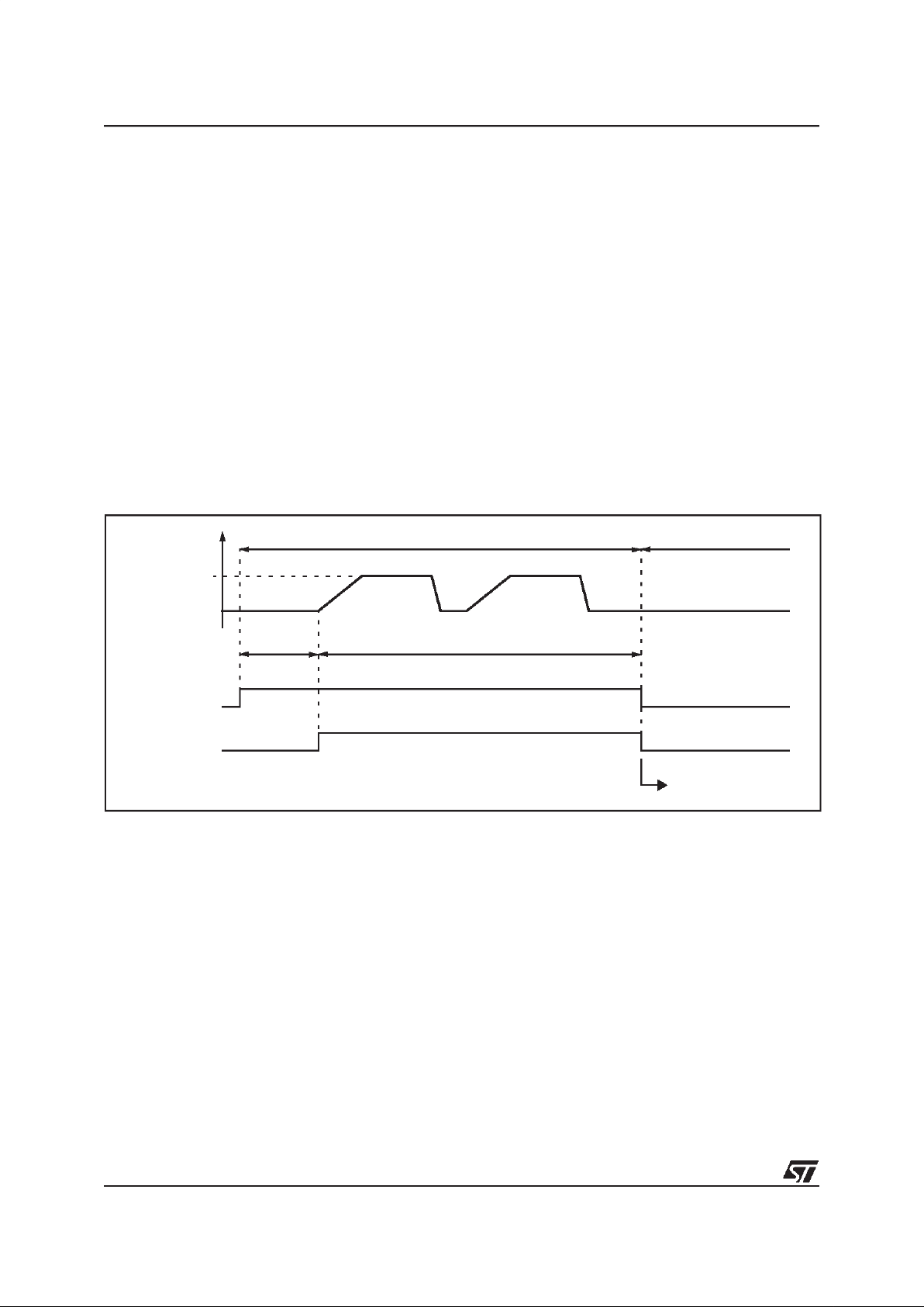
3.5 ACCESS ERROR HANDLING
If a readaccess occurs while LAT=1, thenthe data
bus will not be driven.
If a write access occurs while LAT=0, then the
data on the bus will not be latched.
If a programming cycle is interrupted(by software/
RESET action), the memory data will not be guaranteed.
Figure 6. Data EEPROM Programming Cycle
LAT
ERASE CYCLE WRITE CYCLE
PGM
t
PROG
READ OPERATION NOT POSSIBLE
WRITE OF
DATA LATCHES
READ OPERATION POSSIBLE
INTERNAL
PROGRAMMING
VOLTAGE
EEPROM INTERRUPT

ST72311R, ST72511R, ST72512R, ST72532R
19/164
DATA EEPROM (Cont’d)
3.6 REGISTER DESCRIPTION
CONTROL/STATUS REGISTER (CSR)
Read/Write
Reset Value: 0000 0000 (00h)
Bit 7:3 = Reserved, forced by hardware to 0.
Bit 2 = IE
Interrupt enable
Thisbitisset andclearedby software. Itenablesthe
Data EEPROM interrupt capability when the PGM
bit is cleared byhardware. The interrupt request is
automatically cleared when thesoftware enters the
interrupt routine.
0: Interrupt disabled
1: Interrupt enabled
Bit 1 = LAT
Latch Access Transfer
This bit is set by software. It is cleared by hardware at the end of the programming cycle. It can
only be cleared by software if PGM bit is cleared.
0: Read mode
1: Write mode
Bit 0 = PGM
Programming control and status
Thisbitis set bysoftwaretobegin theprogramming
cycle. At the end of the programming cycle, this bit
isclearedbyhardwareandaninterruptisgenerated
if the ITE bit is set.
0: Programming finished or not yet started
1: Programming cycle is in progress
Note: if the PGM bit is cleared during the programming cycle, the memory data is not guaranteed
Table 3. DATA EEPROM Register Map and Reset Values
70
00000IELATPGM
Address
(Hex.)
Register
Label
76543210
002Ch
EECSR
Reset Value
00000IE0
RWM
0
PGM
0
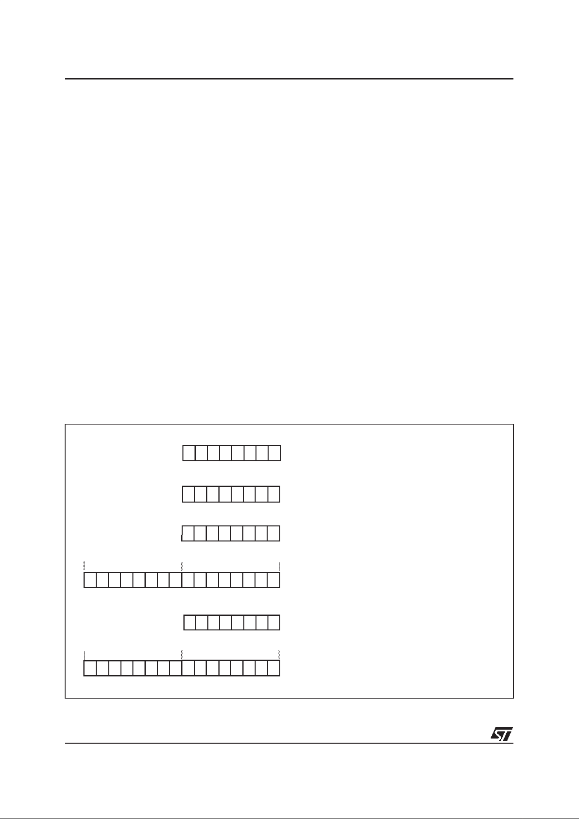
ST72311R, ST72511R, ST72512R, ST72532R
20/164
4 CENTRAL PROCESSING UNIT
4.1 INTRODUCTION
This CPU has a full 8-bit architecture and contains
six internal registers allowing efficient 8-bit data
manipulation.
4.2 MAIN FEATURES
■ Enable executing 63 basic instructions
■ Fast 8-bit by 8-bit multiply
■ 17 main addressing modes (with indirect
addressing mode)
■ Two 8-bit index registers
■ 16-bit stack pointer
■ Low power HALT and WAIT modes
■ Priority maskable hardware interrupts
■ Non-maskable software/hardware interrupts
4.3 CPU REGISTERS
The 6 CPU registers shown in Figure 7 are not
present in the memory mapping andare accessed
by specific instructions.
Accumulator (A)
The Accumulator is an 8-bit general purpose register used to hold operands and the results of the
arithmetic and logic calculations and to manipulate
data.
Index Registers (X and Y)
These 8-bit registers are used to create effective
addresses or as temporary storage areas for data
manipulation. (The Cross-Assembler generates a
precede instruction (PRE) to indicate that the following instruction refers to the Y register.)
The Y register is not affected by theinterrupt automatic procedures.
Program Counter (PC)
The programcounter is a 16-bit register containing
the address of the next instruction to be executed
by the CPU. It is made of two 8-bit registers PCL
(Program CounterLow which is the LSB) and PCH
(Program Counter High which is the MSB).
Figure 7. CPU Registers
ACCUMULATOR
X INDEX REGISTER
Y INDEX REGISTER
STACK POINTER
CONDITION CODE REGISTER
PROGRAM COUNTER
70
1C1I1HI0NZ
RESET VALUE = RESET VECTOR @ FFFEh-FFFFh
70
70
70
0
715 8
PCH
PCL
15
87 0
RESET VALUE = STACKHIGHER ADDRESS
RESET VALUE =
1X11X1XX
RESET VALUE = XXh
RESET VALUE = XXh
RESET VALUE= XXh
X = Undefined Value
ST72311R, ST72511R, ST72512R, ST72532R
21/164
CENTRAL PROCESSING UNIT (Cont’d)
Condition Code Register (CC)
Read/Write
Reset Value: 111x1xxx
The 8-bit Condition Code register contains the interrupt masks and four flags representative of the
result of the instruction just executed. This register
can also be handled by the PUSH and POP instructions.
These bits can be individually tested and/or controlled by specific instructions.
Arithmetic management bits
Bit 4 = H
Half carry
.
This bit is set by hardware whena carry occurs between bits 3 and 4 of the ALU during an ADD or
ADC instructions. It is reset by hardware during
the same instructions.
0: No half carry has occurred.
1: An half carry has occurred.
This bit is tested using the JRH or JRNH instruction. The H bit is useful in BCD arithmetic subroutines.
Bit 2 = N
Negative
.
This bit is set and cleared by hardware. It is representative of the result sign of the last arithmetic,
logical or data manipulation. It’s a copy of the result 7thbit.
0: Theresult of the last operation ispositive or null.
1: The result of the last operation is negative
(i.e. the most significant bit is a logic 1).
This bit is accessed by the JRMI and JRPLinstructions.
Bit 1 = Z
Zero
.
This bit is set and cleared by hardware. This bit indicates that the result of the last arithmetic, logical
or data manipulation is zero.
0: The result of the last operation is different from
zero.
1: The result of the last operation is zero.
This bit is accessed by the JREQ and JRNE test
instructions.
Bit 0 = C
Carry/borrow.
This bit is set and cleared by hardware and software. It indicates an overflow or an underflow has
occurred during the last arithmetic operation.
0: No overflow or underflow has occurred.
1: An overflow or underflow has occurred.
This bit is driven by the SCF and RCF instructions
and tested by theJRC and JRNC instructions. It is
also affected by the “bit test and branch”, shift and
rotate instructions.
Interrupt management bits
Bit 5,3 = I1, I0
Interrupt.
The combination of the Iand I0 bits gives the current interrupt software priority.
These two bits are set/cleared by hardware when
entering in interrupt. The loaded value is given by
the corresponding bits in the interrupt software priority registers (IxSPR). They can be also set/
cleared by software with the RIM, SIM, IRET,
HALT, WFI and PUSH/POP instructions.
See the interrupt management chapter for more
details.
70
11I1HI0NZ
C
Interrupt SoftwarePriority I1 I0
Level 0 (main) 1 0
Level 1 0 1
Level 2 0 0
Level 3 (= interrupt disable) 1 1
ST72311R, ST72511R, ST72512R, ST72532R
22/164
CENTRAL PROCESSING UNIT (Cont’d)
Stack Pointer (SP)
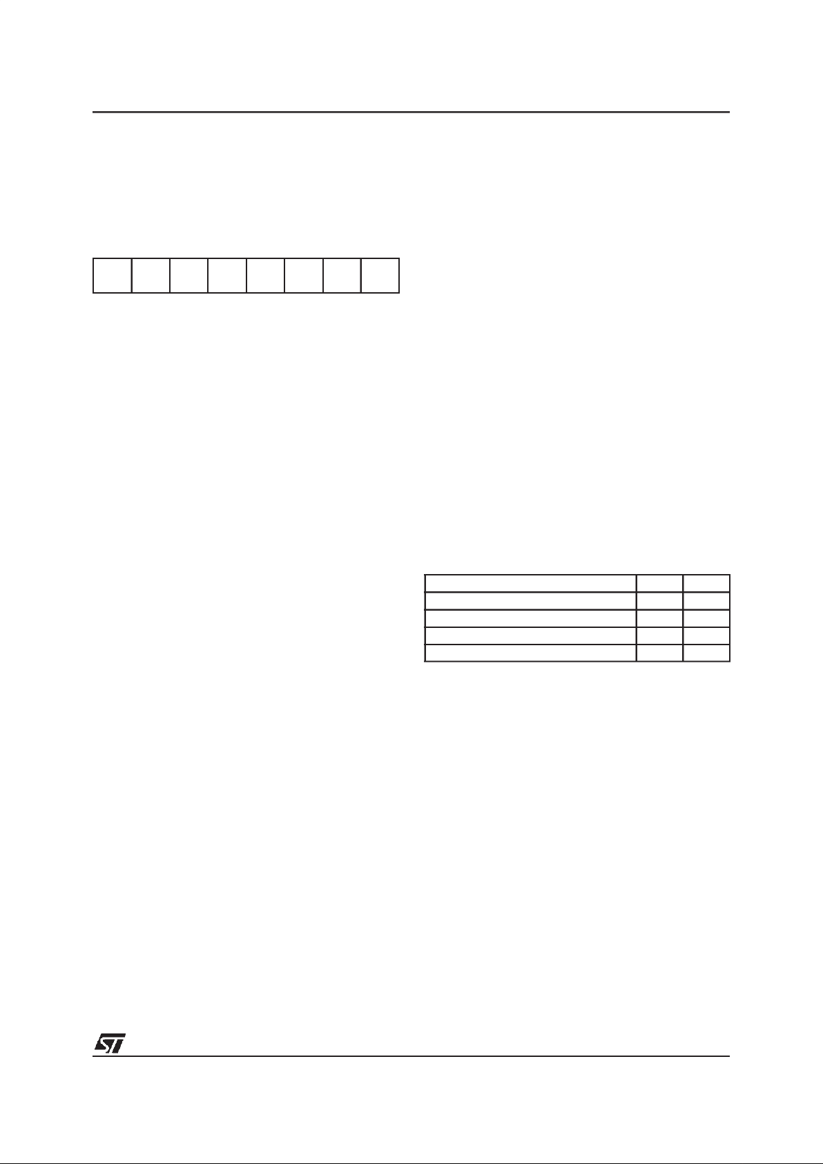
Read/Write
Reset Value: 01 FFh
The Stack Pointer is a 16-bit register which is always pointing to the next free location in the stack.
It is then decremented after data has been pushed
onto the stack and incremented before data is
popped from the stack (see Figure 8).
Since the stack is 256 bytes deep, the 8 most significant bits are forced by hardware. Following an
MCU Reset, or after a Reset Stack Pointer instruction (RSP), the Stack Pointer contains its reset value (the SP7 to SP0 bits are set) which is the stack
higher address.
The least significant byte of the Stack Pointer
(called S) can be directly accessed by a LD instruction.
Note: When the lower limit is exceeded, the Stack
Pointer wraps around to the stackupper limit, without indicating the stack overflow. The previously
stored information is then overwritten and therefore lost.The stack also wraps in caseof anunderflow.
The stack is used to save the return address during a subroutine call and the CPU context during
an interrupt. The user may also directly manipulate
the stack by means of the PUSH and POP instructions. In the case of an interrupt, the PCL is stored
at the first location pointed to by the SP. Then the
other registers are stored in the next locations as
shown in Figure 8
– When an interrupt is received, the SP is decre-
mented and the context is pushed on the stack.
– On return frominterrupt, the SP is incremented
and the context is popped from the stack.
A subroutine call occupies twolocations and an interrupt five locations in the stack area.
Figure 8. Stack Manipulation Example
15 8
00000001
70
SP7 SP6 SP5 SP4 SP3 SP2 SP1 SP0
PCH
PCL
SP
PCH
PCL
SP
PCL
PCH
X
A
CC
PCH
PCL
SP
PCL
PCH
X
A
CC
PCH
PCL
SP
PCL
PCH
X
A
CC
PCH
PCL
SP
SP
Y
CALL
Subroutine
Interrupt
Event
PUSH Y POP Y IRET
RET
or RSP
@ 01FFh
@ 0100h
Stack Higher Address = 01FFh
Stack Lower Address =
0100h
ST72311R, ST72511R, ST72512R, ST72532R
23/164
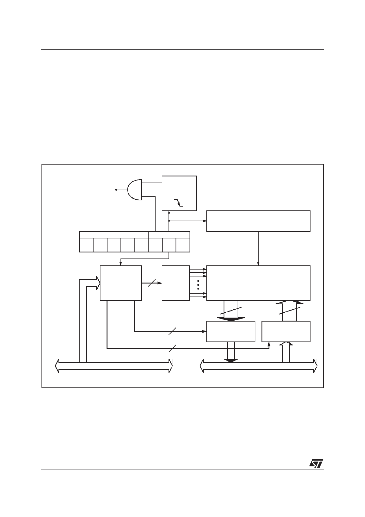
5 SUPPLY, RESET AND CLOCK MANAGEMENT
The ST72311R, ST72511R, ST72512R and
ST72532R microcontrollers include a range of utility features for securing the application in critical
situations (for example in case of a power brownout), and reducing the number of external components. An overview is shown in Figure 9.
Main features
■ Main supply low voltage detection (LVD)
■ RESET Manager (RSM)
■ Low consumption resonator oscillator
Figure 9. Clock, RESET, Option and Supply Management Overview
f
OSC
LOW VOLTAGE
DETECTOR
(LVD)
FROM
WATCHDOG
PERIPHERAL
OSC2
OSC1
RESET
V
DD
V
SS
OSCILLATOR
RESET
TO
MAIN CLOCK
CONTROLLER
ST72311R, ST72511R, ST72512R, ST72532R
24/164
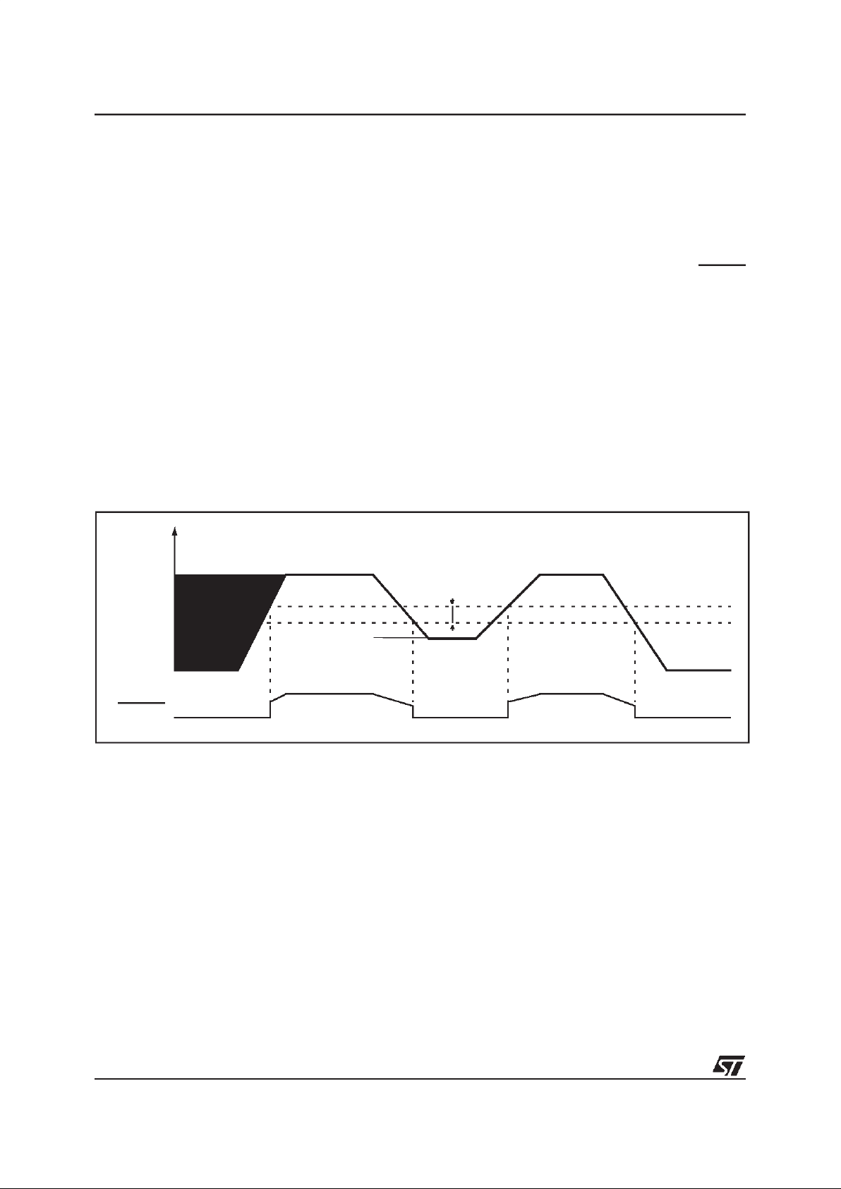
5.1 LOW VOLTAGE DETECTOR (LVD)
To allow the integration of power management
features in theapplication, the Low Voltage Detector function (LVD) generates a static reset when
the VDDsupply voltage is below a V
IT-
reference
value. This means that it secures the power-up as
well as the power-down keeping the ST7 in reset.
The V
IT-
referencevalue for a voltage drop is lower
than the V
IT+
referencevalue for power-on in order
to avoida parasitic reset when theMCU starts running and sinks current on the supply (hysteresis).
The LVD Reset circuitry generates a reset when
VDDis below:
–V
IT+
when VDDis rising
–V
IT-
when VDDis falling
The LVD function is illustrated in Figure 10.
Provided the minimum VDDvalue (guaranteed for
the oscillator frequency) is below V
IT-
, the MCU
can onlybe in two modes:
– under full software control
– in static safe reset
In these conditions, secure operation is always ensured for the application without the need for external reset hardware.
During a Low Voltage Detector Reset, the RESET
pin is held low, thus permitting the MCU to reset
other devices.
Notes:
The LVD allows the device to be used without any
external RESET circuitry.
The LVD is an optional function which can be se-
lected whenordering the device (ordering information).
Figure 10. Low Voltage Detector vs Reset
V
DD
V
IT+
RESET
V
IT-
V
hys
ST72311R, ST72511R, ST72512R, ST72532R
25/164
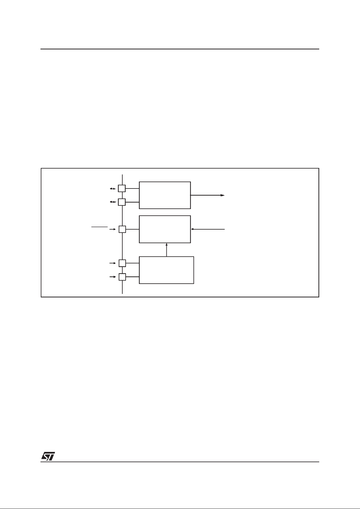
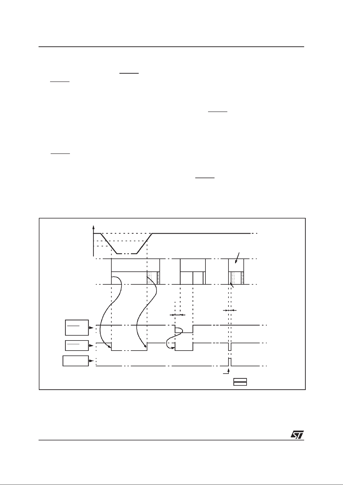
5.2 RESET SEQUENCE MANAGER (RSM)
5.2.1 Introduction
The reset sequence manager includes three RESET sources as shown in Figure 12:
■ External RESET source pulse
■ Internal LVD RESET (Low Voltage Detection)
■ Internal WATCHDOG RESET
These sources act on the RESET pin and it is always kept low during the delay phase.
The RESET service routine vector is fixed at addresses FFFEh-FFFFh in the ST7 memory map.
The basic RESET sequence consists of 3 phases
as shown in Figure11:
■ Delay depending on the RESET source
■ 4096 CPU clock cycle delay
■ RESET vector fetch
The 4096 CPU clock cycle delay allows the oscillator to stabilise and ensures that recovery has
taken place from the Reset state.
The RESET vector fetch phase duration is 2 clock
cycles.
Figure 11. RESET Sequence Phases
Figure 12. Reset Block Diagram
RESET
DELAY
INTERNAL RESET
4096 CLOCKCYCLES
FETCH
VECTOR
f
CPU
COUNTER
RESET
R
ON
V
DD
WATCHDOG RESET
LVD RESET
INTERNAL
RESET
ST72311R, ST72511R, ST72512R, ST72532R
26/164
RESET SEQUENCE MANAGER (Cont’d)
5.2.2 Asynchronous External RESET pin
The RESET pin is both an input andan open-drain
output with integrated RONweak pull-up resistor.
This pull-up has no fixed value but varies in accordance with the input voltage. It can be pulled
low by external circuitry to reset the device. See
electrical characteristics section for more details.
A RESET signal originating from an external
source must have a duration of atleast t
h(RSTL)in
in
order to berecognized as shown in Figure 13. This
detection is asynchronous and therefore the MCU
can enterreset state even in HALT mode.
The RESET pin is an asynchronous signal which
plays a major role in EMS performance. In a noisy
environment, it is recommended to follow the
guidelines mentioned in the electrical characteristics section.
5.2.3 Internal Low Voltage Detection RESET
Two different RESET sequences caused by the internal LVD circuitry can be distinguished:
■ Power-On RESET
■ Voltage Drop RESET
The device RESET pin acts as an output that is
pulled low when VDD<V
IT+
(rising edge) or
VDD<V
IT-
(falling edge)as shown in Figure 13.
The LVD filters spikes on VDDlarger than t
g(VDD)
to
avoid parasitic resets.
5.2.4 Internal WatchdogRESET
The RESET sequence generated by a internal
Watchdog counter overflow is shown in Figure 13.
Starting fromthe Watchdog counter underflow, the
device RESET pin acts as an output that is pulled
low during t
w(RSTL)out
.
CAUTION: this output signal as not enought energy to be used to drive external devices.
Figure 13. RESET Sequences
V
DD
RUN
RESET PIN
EXTERNAL
WATCHDOG
DELAY
V
IT+
V
IT-
t
h(RSTL)in
RUN
DELAY
WATCHDOG UNDERFLOW
t
w(RSTL)out
RUN
DELAY
RUN
RESET
RESET
SOURCE
SHORT EXT.
RESET
LVD
RESET
WATCHDOG
RESET
INTERNAL RESET (4096T
CPU
)
FETCH VECTOR
ST72311R, ST72511R, ST72512R, ST72532R
27/164
5.3 LOW CONSUMPTION OSCILLATOR
The f
OSC
main clock of the ST7 can be generated
by two different source types:
■ an external source
■ a crystal or ceramic resonator oscillators
The associated hardware configuration are shown
in Table 4. Refer to the electrical characteristics
section for more details.
External Clock Source
In this external clock mode, a clock signal (square,
sinus or triangle) with ~50% duty cycle has to drive
the OSC1pin while the OSC2 pinis tied to ground.
Crystal/Ceramic Oscillator
This oscillator (based on constant current source)
is optimized in terms of consumption and has the
advantage of producing a very accurate rate on
the main clock of the ST7.
When using this oscillator, the resonator and the
load capacitances have to be connected as shown
in Table 4 and have to be mounted as close as
possible to the oscillator pins in order to minimize
output distortion and start-up stabilization time.
This oscillator is not stopped during the RESET
phase to avoid losing time in the oscillator start-up
phase.
These oscillators are not stopped during the
RESET phase to avoid losing time in the oscillator
start-up phase.
Table 4. ST7 Clock Sources
Hardware Configuration
External ClockCrystal/Ceramic Resonators
OSC1 OSC2
EXTERNAL
ST7
SOURCE
V
DD
R
OBP
OSC1 OSC2
LOAD
CAPACITORS
ST7
C
L2
C
L1
ST72311R, ST72511R, ST72512R, ST72532R
28/164
6 INTERRUPTS
6.1 INTRODUCTION
The ST7 enhanced interrupt management provides the following features:
■ Hardware interrupts
■ Software interrupt (TRAP)
■ Nested or concurrent interrupt management
with flexible interrupt priority and level
management:
– Up to 4 software programmable nesting levels
– Up to 16 interrupt vectors fixed by hardware
– 3 non maskable events: TLI, RESET, TRAP
This interrupt management is based on:
– Bit 5 and bit 3 of the CPU CC register (I1:0),
– Interrupt software priority registers (ISPRx),
– Fixed interrupt vector addresses located at the
high addresses of the memory map (FFE0h to
FFFFh) sorted by hardware priority order.
This enhanced interrupt controller guarantees full
upward compatibility with the standard (not nested) ST7 interrupt controller.
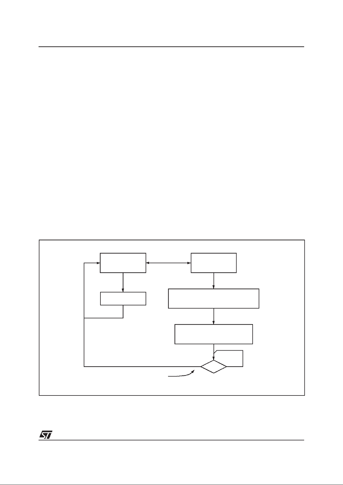
6.2 MASKING AND PROCESSING FLOW
The interrupt masking is managed by the I1and I0
bits of the CC register and the ISPRx registers
which give the interrupt software priority level of
each interrupt vector (see Table 5). The processing flow is shown in Figure 14
When an interrupt request has to be serviced:
– Normal processing is suspended at the end of
the current instruction execution.
– The PC, X, A and CC registers are saved onto
the stack.
– I1 and I0 bits of CC register are set according to
the corresponding values in the ISPRx registers
of the serviced interrupt vector.
– ThePC isthen loadedwith the interrupt vector of
the interrupt to service and the first instruction of
the interrupt service routine is fetched (refer to
“Interrupt Mapping” table for vector addresses).
The interrupt service routine should end with the
IRET instruction which causes the contents of the
saved registers to be recovered from the stack.
Note: As a consequence of the IRET instruction,
the I1 and I0 bits will be restored from the stack
and the program in the previous level will resume.
Table 5. Interrupt Software Priority Levels
Figure 14. Interrupt Processing Flowchart
Interrupt software priority Level I1 I0
Level 0 (main) Low
High
10
Level 1 0 1
Level 2 0 0
Level 3 (= interrupt disable) 1 1
“IRET”
RESTORE PC,X, A,CC
STACK PC, X, A, CC
LOAD I1:0 FROM INTERRUPT SW REG.
FETCH NEXT
RESET
TLI
PENDING
INSTRUCTION
I1:0
FROM STACK
LOAD PC FROM INTERRUPT VECTOR
Y
N
Y
N
Y
N
Interrupt has the same or a
lower software priority
THE INTERRUPT
STAYS PENDING
than current one
Interrupt has a higher
software priority
than current one
EXECUTE
INSTRUCTION
INTERRUPT
ST72311R, ST72511R, ST72512R, ST72532R
29/164
INTERRUPTS (Cont’d)
Servicing Pending Interrupts
As several interrupts can be pending at the same
time, theinterrupt to be taken into account is determined by the following two-step process:
– the highestsoftware priority interrupt is serviced,
– if several interrupts have the same software pri-
ority thenthe interrupt with the highest hardware
priority is serviced first.
Figure 15 describes this decision process.
Figure 15. Priority Decision Process
When an interrupt request is not serviced immediately, it is latched and then processed when its
software priority combined with the hardware priority becomes the highest one.
Note 1: The hardware priority is exclusive while
the software one is not. This allows the previous
process to succeed with only one interrupt.
Note 2: RESET, TRAP and TLI are non maskable
and they can be considered as having the highest
software priority in the decision process.
Different Interrupt Vector Sources
Two interrupt source types are managed by the
ST7 interrupt controller: the non-maskable type
(RESET, TLI, TRAP) and the maskable type (external or from internal peripherals).
Non-Maskable Sources
These sources are processed regardless of the
state of the I1 and I0 bits of the CC register (see
Figure 14). After stacking the PC, X, A and CC
registers (except for RESET), the corresponding
vector is loaded in the PC register and the I1 and
I0 bits of the CC are set to disable interrupts (level
3). These sources allow the processor to exit
HALT mode.
■ TLI (Top Level Hardware Interrupt)
This hardware interrupt occurs when a specific
edge is detected on the dedicated TLI pin. Its detailed specification is given in the Miscellaneous
register chapter.
■ TRAP (Non Maskable Software Interrupt)
This software interrupt is serviced when the TRAP
instruction is executed. It will be serviced according to the flowchart on Figure 14 as a TLI.
■ RESET
The RESET source has the highest priority in the
ST7. This means that the first current routine has
the highest software priority (level 3) and thehighest hardware priority.
See the RESET chapter for more details.
Maskable Sources
Maskable interrupt vector sourcescan be serviced
if the corresponding interrupt is enabled and if its
own interrupt software priority (in ISPRx registers)
is higher than the one currently being serviced (I1
and I0 in CC register). If any of these two conditions is false, the interrupt is latched and thus remains pending.
■ External Interrupts
External interrupts allow the processor to exit from
HALT low power mode.
External interrupt sensitivity is softwareselectable
through the Miscellaneous registers (MISCRx).
External interrupt triggeredon edge will be latched
and the interrupt request automatically cleared
upon entering the interrupt service routine.
If several input pins of a group connected to the
same interrupt line are selected simultaneously,
these will be logically ORed.
■ Peripheral Interrupts
Usually the peripheral interrupts cause the MCU to
exit from HALT mode except those mentioned in
the “Interrupt Mapping” table.
A peripheral interrupt occurs when a specific flag
is set in the peripheral status registers and if the
corresponding enable bit is set in the peripheral
control register.
The general sequence for clearing an interrupt is
based on an access to the status register followed
by a read or write to an associated register.
Note: The clearing sequence resets the internal
latch. A pending interrupt (i.e. waiting for being
serviced) will therefore be lost if the clear sequence is executed.
PENDING
SOFTWARE
Different
INTERRUPTS
Same
HIGHESTHARDWARE
PRIORITY SERVICED
PRIORITY
HIGHEST SOFTWARE
PRIORITY SERVICED
ST72311R, ST72511R, ST72512R, ST72532R
30/164
INTERRUPTS (Cont’d)
6.3 INTERRUPTS AND LOW POWER MODES
All interrupts allow the processor to exit the WAIT
low power mode. On the contrary, only external
and other specified interrupts allow the processor
to exit the HALT modes (see column “Exit from
HALT” in“Interrupt Mapping” table). When several
pending interrupts are present while exiting HALT
mode, the first one serviced can only be an interrupt with exit from HALT mode capability and it is
selected through the same decision process
shown in Figure 15
Note: If an interrupt, that is not able to Exit from
HALT mode, is pending with the highest priority
when exiting HALT mode, this interrupt is serviced
after the first one serviced.
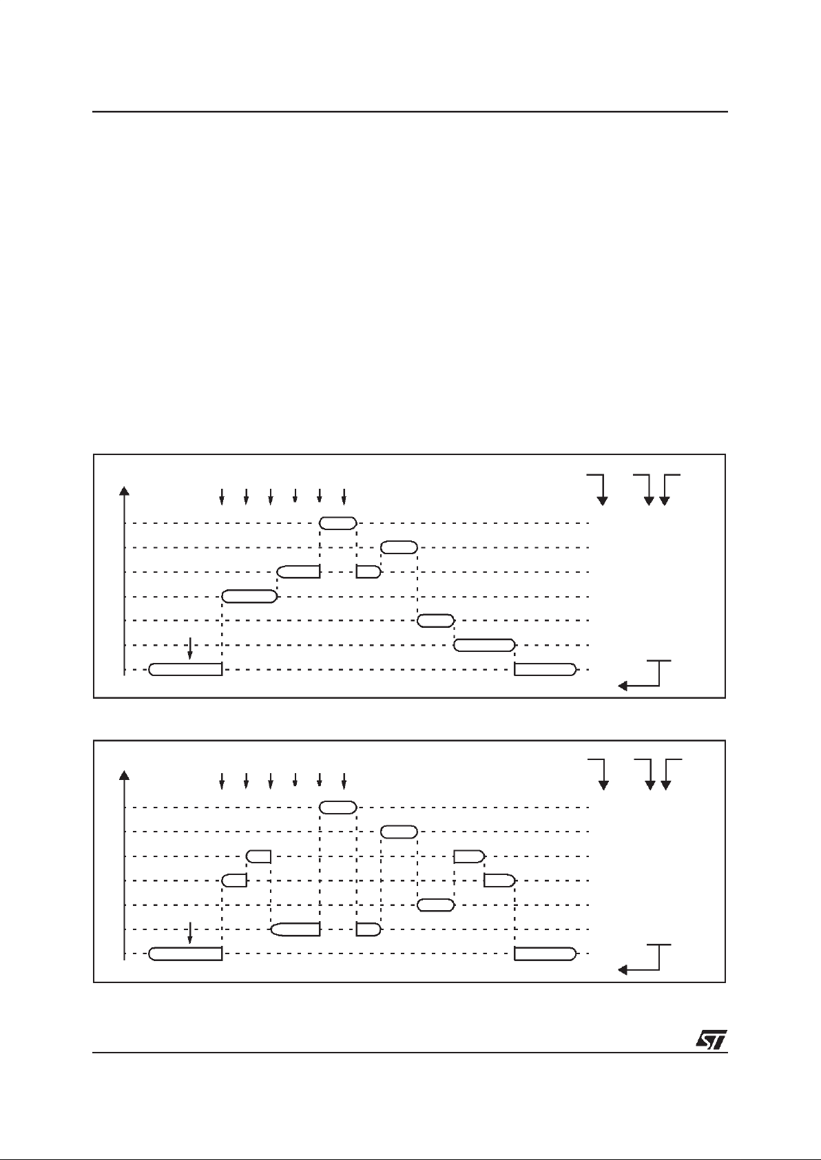
6.4 CONCURRENT & NESTED MANAGEMENT
The following Figure 16 and Figure 17 show two
different interrupt management modes. The first is
called concurrent mode and does not allow an interrupt to be interrupted, unlike the nested mode in
Figure 17 The interrupt hardware priority is given
in this order from the lowest to the highest: MAIN,
IT4, IT3, IT2, IT1, IT0,TLI. The software priority is
given for each interrupt.
Warning: A stack overflow may occur without notifying the software of the failure.
Figure 16. Concurrent interrupt management
Figure 17. Nested interrupt management
MAIN
IT4
IT2
IT1
TLI
IT1
MAIN
IT0
I1
HARDWARE PRIORITY
SOFTWARE
3
3
3
3
3
3/0
3
11
11
11
11
11
11 / 10
11
RIM
IT2
IT1
IT4
TLI
IT3
IT0
IT3
I0
10
PRIORITY
LEVEL
USED STACK = 10 BYTES
MAIN
IT2
TLI
MAIN
IT0
IT2
IT1
IT4
TLI
IT3
IT0
HARDWARE PRIORITY
3
2
1
3
3
3/0
3
11
00
01
11
11
11
RIM
IT1
IT4 IT4
IT1
IT2
IT3
I1 I0
11 / 10 10
SOFTWARE
PRIORITY
LEVEL
USED STACK = 20 BYTES

ST72311R, ST72511R, ST72512R, ST72532R
31/164
INTERRUPTS (Cont’d)
6.5 INTERRUPT REGISTER DESCRIPTION
CPU CC REGISTER INTERRUPT BITS
Read/Write
Reset Value: 111x 1010 (xAh)
Bit 5, 3 = I1, I0
Software Interrupt Priority
These two bits indicate the current interrupt software priority.
These two bits are set/cleared by hardware when
entering in interrupt. The loaded value is given by
the corresponding bits in the interrupt software priority registers (ISPRx).
They can be also set/cleared by software with the
RIM, SIM, HALT, WFI, IRET and PUSH/POP instructions (see “Interrupt Dedicated Instruction
Set” table).
*Note: TLI, TRAP and RESET events are non
maskable sources and can interrupt a level 3 program.
INTERRUPT SOFTWARE PRIORITY REGISTERS (ISPRX)
Read/Write (bit 7:4 of ISPR3 are read only)
Reset Values: 1111 1111 (FFh)
These four registers contain the interrupt software
priority of each interrupt vector.
– Eachinterruptvector (exceptRESET andTRAP)
has corresponding bits in these registers where
its own software priority is stored. This correspondance is shown in the following table.
– Each I1_x and I0_x bit value in the ISPRx regis-
ters has the same meaning as the I1 and I0 bits
in the CC register.
– Level 0 can not be written (I1_x=1, I0_x=0). In
this case,the previouslystored value is kept. (example: previous=CFh, write=64h, result=44h)
The RESET, TRAP and TLI vectors have no software priorities. When one is serviced, the I1 and I0
bits of the CC register are both set.
*Note: Bits in the ISPRx registers which correspond to the TLI can be read and written but they
are not significant in the interrupt process management.
Caution: If the I1_x and I0_x bits are modified
while the interrupt x is executed the following behaviour has to be considered: If the interrupt x is
still pending (new interrupt or flag not cleared) and
the new software priority is higher than the previous one, the interrupt x is re-entered. Otherwise,
the software priority stays unchanged up to the
next interrupt request (after the IRET of the interrupt x).
70
11I1 H I0 NZC
Interrupt Software Priority Level I1 I0
Level 0 (main)
Low
High
10
Level 1 0 1
Level 2 0 0
Level 3 (= interrupt disable*) 1 1
70
ISPR0 I1_3 I0_3 I1_2 I0_2 I1_1 I0_1 I1_0 I0_0
ISPR1 I1_7 I0_7 I1_6 I0_6 I1_5 I0_5 I1_4 I0_4
ISPR2 I1_11 I0_11 I1_10 I0_10 I1_9 I0_9 I1_8 I0_8
ISPR3 1 1 1 1 I1_13 I0_13 I1_12 I0_12
Vector address ISPRx bits
FFFBh-FFFAh I1_0 and I0_0 bits*
FFF9h-FFF8h I1_1 and I0_1 bits
... ...
FFE1h-FFE0h I1_13 and I0_13 bits

ST72311R, ST72511R, ST72512R, ST72532R
32/164
INTERRUPTS (Cont’d)
Table 6. Dedicated Interrupt Instruction Set
Note: During the execution of an interrupt routine, the HALT, POPCC, RIM, SIM and WFI instructions change the current
software priority up to the next IRET instruction or one of the previously mentioned instructions.
In order not to lose the current software priority level, the RIM, SIM, HALT, WFI and POP CC instructions should never
be used in an interrupt routine.
Table 7. Interrupt Mapping
Instruction New Description Function/Example I1 H I0 N Z C
HALT Entering Halt mode 1 0
IRET Interrupt routine return Pop CC, A, X, PC I1 H I0 N Z C
JRM Jump if I1:0=11 I1:0=11 ?
JRNM Jump if I1:0<>11 I1:0<>11 ?
POP CC Pop CC from the Stack Mem => CC I1 H I0 N Z C
RIM Enable interrupt (level 0 set) Load 10 in I1:0 of CC 1 0
SIM Disable interrupt (level 3 set) Load 11 in I1:0 of CC 1 1
TRAP Software trap Software NMI 1 1
WFI Wait for interrupt 1 0
N°
Source
Block
Description
Register
Label
Priority
Order
Exit
from
HALT
Address
Vector
RESET Reset
N/A
Highest
Priority
Lowest
Priority
yes FFFEh-FFFFh
TRAP Software Interrupt no FFFCh-FFFDh
0 TLI External Top Level Interrupt MISCR2 yes FFFAh-FFFBh
1 MCC/RTC Main Clock Controller Time Base Interrupt MCCSR FFF8h-FFF9h
2 ei0 External Interrupt Port A3..0
N/A
FFF6h-FFF7h
3 ei1 External Interrupt Port F2..0 FFF4h-FFF5h
4 ei2 External Interrupt Port B3..0 FFF2h-FFF3h
5 ei3 External Interrupt Port B7..4 FFF0h-FFF1h
6 CAN CAN Peripheral Interrupts CANISR FFEEh-FFEFh
7 SPI SPI Peripheral Interrupts SPISR
no
FFECh-FFEDh
8 TIMER A TIMER A Peripheral Interrupts TASR FFEAh-FFEBh
9 TIMER B TIMER B Peripheral Interrupts TBSR FFE8h-FFE9h
10 SCI SCI Peripheral Interrupts SCISR FFE6h-FFE7h
11 EEPROM EEPROM Interrupt EECSR FFE4h-FFE5h
12 Not Used FFE2h-FFE3h
13 PWM ART PWM ART Overflow Interrupt ARTCSR Yes FFE0h-FFE1h

ST72311R, ST72511R, ST72512R, ST72532R
33/164
INTERRUPTS (Cont’d)
Table 8. Nested Interrupts Register Map and Reset Values
Address
(Hex.)
Register
Label
76543210
0024h
ISPR0
Reset Value
ei1 ei0 MCC/RTC TLI
I1_3
1
I0_3
1
I1_2
1
I0_2
1
I1_1
1
I0_1
111
0025h
ISPR1
Reset Value
SPI CAN ei3 ei2
I1_7
1
I0_7
1
I1_6
1
I0_6
1
I1_5
1
I0_5
1
I1_4
1
I0_4
1
0026h
ISPR2
Reset Value
EEPROM SCI TIMER B TIMER A
I1_11
1
I0_11
1
I1_10
1
I0_10
1
I1_9
1
I0_9
1
I1_8
1
I0_8
1
0027h
ISPR3
Reset Value 1 1 1 1
PWMART Not Used
I1_13
1
I0_13
1
I1_12
1
I0_12
1

ST72311R, ST72511R, ST72512R, ST72532R
34/164
7 POWER SAVING MODES
7.1 INTRODUCTION
To give alarge measure of flexibility to the application in terms of power consumption, four main
power saving modes are implemented in the ST7
(see Figure 18): SLOW, WAIT (SLOW WAIT), ACTIVE HALT and HALT.
After a RESET the normal operating mode is selected by default (RUN mode). This mode drives
the device (CPU and embedded peripherals) by
means of a master clock which is based on the
main oscillator frequency divided by 2 (f
CPU
).
From RUN mode, the different power saving
modes may be selected by setting the relevant
register bits or by calling the specificST7 software
instruction whose action depends on the the oscillator status.
Figure 18. Power Saving Mode Transitions
7.2 SLOW MODE
This mode has two targets:
– Toreduce power consumption bydecreasingthe
internal clock in the device,
– To adapt the internal clock frequency (f
CPU
)to
the available supply voltage.
SLOW mode is controlled by three bits in the
MISCR1 register: the SMS bit which enables or
disables Slow modeand two CPx bits which select
the internal slow frequency (f
CPU
).
In this mode, the oscillator frequency can be divided by 4, 8, 16 or 32 instead of 2 in normal operating mode.The CPU and peripherals are clocked at
this lower frequency.
Note: SLOW-WAIT mode is activated when enterring the WAIT mode while the device is already in
SLOW mode.
Figure 19. SLOW Mode Clock Transitions
POWER CONSUMPTION
WAIT
SLOW
RUN
ACTIVE HALT
High
Low
SLOW WAIT
HALT
00 01
SMS
CP1:0
f
CPU
NEW SLOW
NORMAL RUN MODE
MISCR1
FREQUENCY
REQUEST
REQUEST
f
OSC
/2
f
OSC
/4 f
OSC
/8 f
OSC
/2

ST72311R, ST72511R, ST72512R, ST72532R
35/164
POWER SAVING MODES (Cont’d)
7.3 WAIT MODE
WAIT mode places the MCU in a low power consumption mode by stopping the CPU.
This power saving mode is selected by calling the
‘WFI’ instruction.
All peripherals remain active. During WAIT mode,
the I[1:0] bits of the CC register are forced to ‘10’,
to enable all interrupts. All other registers and
memory remain unchanged. The MCU remains in
WAIT mode until an interrupt or RESET occurs,
whereupon the Program Counter branches to the
starting address of the interrupt or Reset service
routine.
The MCU will remain in WAIT mode until a Reset
or an Interrupt occurs, causing it to wake up.
Refer to Figure 20.
Figure 20. WAIT Mode Flow-chart
Note:
1. Before servicing an interrupt, the CC register is
pushed on the stack. The I[1:0] bits of the CC register are set to the current software priority level of
the interrupt routine and recovered when the CC
register is popped.
WFI INSTRUCTION
RESET
INTERRUPT
Y
N
N
Y
CPU
OSCILLATOR
PERIPHERALS
I[1:0] BITS
ON
ON
10
OFF
FETCH RESET VECTOR
OR SERVICE INTERRUPT
CPU
OSCILLATOR
PERIPHERALS
I[1:0] BITS
ON
OFF
10
ON
CPU
OSCILLATOR
PERIPHERALS
I[1:0] BITS
ON
ON
XX
1)
ON
4096 CPU CLOCK CYCLE
DELAY

ST72311R, ST72511R, ST72512R, ST72532R
36/164
POWER SAVING MODES (Cont’d)
7.4 ACTIVE-HALT AND HALT MODES
ACTIVE-HALT and HALT modes are the two lowest power consumption modes of the MCU. They
are both entered by executing the ‘HALT’ instruction. The decision to enter either in ACTIVE-HALT
or HALT mode is given by the MCC/RTC interrupt
enable flag (OIE bit in MCCSR register).
7.4.1 ACTIVE-HALT MODE
ACTIVE-HALT mode is the lowest power consumption mode of the MCU with a real time clock
available. It is entered by executing the ‘HALT’ instruction when the OIE bit of the Main Clock Controller Status register (MCCSR) is set (see Section
10.2 on page 52 for more details on the MCCSR
register).
The MCU can exit ACTIVE-HALT mode on reception of either an MCC/RTC interrupt, a specific interrupt (see Table 7, “Interrupt Mapping,” on
page 32) or a RESET. When exiting ACTIVEHALT mode by means of a RESETor an interrupt,
a 4096 CPU cycle delay occurs. After the start up
delay, the CPU resumes operation by servicing
the interrupt or by fetching the reset vector which
woke it up (see Figure 22).
When entering ACTIVE-HALT mode,the I[1:0] bits
in the CC register are forced to ‘10’ to enable interrupts. Therefore, if an interrupt is pending, the
MCU wakes up immediately.
In ACTIVE-HALT mode, only the main oscillator
and its associated counter (MCC/RTC) are running tokeep a wake-uptime base. All other peripherals are not clocked except those which get their
clock supply from another clock generator (such
as external or auxiliary oscillator).
The safeguard against staying locked in ACTIVEHALT mode is provided by the oscillator interrupt.
Note: As soon asthe interrupt capability of one of
the oscillators is selected (MCCSR.OIE bit set),
entering ACTIVE-HALT mode while the Watchdog
is active does not generate a RESET.
This means that the device cannot spend more
than a defined delay in this power saving mode.
Figure 21. ACTIVE-HALT TimingOverview
Figure 22. ACTIVE-HALT Mode Flow-chart
Notes:
1. Peripheral clocked with anexternal clock source
can still be active.
2. Only the MCC/RTC interrupt and some specific
interrupts can exit the MCU from ACTIVE-HALT
mode (such as external interrupt). Refer to
Table 7, “Interrupt Mapping,” on page 32 for more
details.
3. Before servicing an interrupt, the CC register is
pushed on the stack. The I[1:0] bits of the CC register are set to the current software priority level of
the interrupt routine and restored when the CC
register is popped.
MCCSR
OIE bit
Power Saving Mode entered when HALT
instruction is executed
0 HALT mode
1 ACTIVE-HALT mode
HALTRUN RUN
4096 CPU CYCLE
DELAY
RESET
OR
INTERRUPT
HALT
INSTRUCTION
FETCH
VECTOR
ACTIVE
[MCCSR.OIE=1]
HALT INSTRUCTION
RESET
INTERRUPT
2)
Y
N
N
Y
CPU
OSCILLATOR
PERIPHERALS
1)
I[1:0] BITS
ON
OFF
10
OFF
FETCH RESET VECTOR
OR SERVICE INTERRUPT
CPU
OSCILLATOR
PERIPHERALS
I[1:0] BITS
ON
OFF
XX
3)
ON
CPU
OSCILLATOR
PERIPHERALS
I[1:0] BITS
ON
ON
XX
3)
ON
4096 CPU CLOCK CYCLE
DELAY
(MCCSR.OIE=1)

ST72311R, ST72511R, ST72512R, ST72532R
37/164
POWER SAVING MODES (Cont’d)
7.4.2 HALT MODE
The HALT mode is the lowest power consumption
mode of the MCU. It is entered by executing the
‘HALT’ instruction when the OIE bit of the Main
Clock Controller Status register (MCCSR) is
cleared (see Section 10.2 on page 52 for more details on the MCCSR register).
The MCU can exit HALT mode on reception of either a specific interrupt (see Table 7, “Interrupt
Mapping,” on page 32) or a RESET. When exiting
HALT mode by means of a RESETor an interrupt,
the oscillator is immediately turned on and the
4096 CPU cycle delay is used to stabilize the oscillator. After the start up delay, the CPU resumes
operation by servicing the interrupt or by fetching
the reset vector which woke it up (see Figure 24).
When entering HALT mode, the Ibit in the CC register is forced to 0 to enable interrupts. Therefore,
if an interrupt is pending, the MCU wakes immediately.
In HALT mode, the main oscillator is turned off
causing all internal processing to be stopped, including the operation of the on-chip peripherals.
All peripherals are not clocked except the ones
which get their clock supply from another clock
generator (such as an external or auxiliary oscillator).
The compatibility of Watchdog operation with
HALT mode is configured by the “WDGHALT” option bit of the option byte. The HALT instruction
when executed while the Watchdog system is enabled, can generate a Watchdog RESET (see
Section 14.1 on page 158 for more details).
Figure 23. HALT Timing Overview
Figure 24. HALT Mode Flow-chart
Notes:
1. WDGHALT is anoption bit. See option byte sec-
tion for more details.
2. Peripheral clocked with anexternal clock source
can still be active.
3. Only some specific interrupts can exit the MCU
from HALT mode (such as external interrupt). Refer to Table 7, “Interrupt Mapping,” on page 32 for
more details.
4. Before servicing an interrupt, the CC register is
pushed on the stack. The I[1:0] bits of the CC register are set to the current software priority level of
the interrupt routine and recovered when the CC
register is popped.
HALTRUN RUN
4096 CPU CYCLE
DELAY
RESET
OR
INTERRUPT
HALT
INSTRUCTION
FETCH
VECTOR
[MCCSR.OIE=0]
HALT INSTRUCTION
RESET
INTERRUPT
3)
Y
N
N
Y
CPU
OSCILLATOR
PERIPHERALS
2)
I[1:0] BITS
OFF
OFF
10
OFF
FETCH RESET VECTOR
OR SERVICE INTERRUPT
CPU
OSCILLATOR
PERIPHERALS
I[1:0] BITS
ON
OFF
XX
4)
ON
CPU
OSCILLATOR
PERIPHERALS
I[1:0] BITS
ON
ON
XX
4)
ON
4096 CPU CLOCK CYCLE
DELAY
WATCHDOG
ENABLE
DISABLE
WDGHALT
1)
0
WATCHDOG
RESET
1
(MCCSR.OIE=0)

ST72311R, ST72511R, ST72512R, ST72532R
38/164
8 I/O PORTS
8.1 INTRODUCTION
The I/O ports offer different functional modes:
– transferof data through digitalinputs and outputs
and for specific pins:
– external interrupt generation
– alternate signal input/output for the on-chip pe-
ripherals.
An I/O port contains up to 8 pins. Each pin can be
programmed independently as digital input(with or
without interrupt generation) or digital output.
8.2 FUNCTIONAL DESCRIPTION
Each port has 2 main registers:
– Data Register (DR)
– Data Direction Register (DDR)
and one optional register:
– Option Register (OR)
Each I/O pin may be programmed using the corre-
sponding register bits in the DDR and OR registers: bit X corresponding to pin X of the port. The
same correspondence is used for the DR register.
The following description takes into account the
OR register, (for specific ports which do not provide this register refer to the I/O Port Implementation section). The generic I/O block diagram is
shown in Figure 25
8.2.1 Input Modes
The input configuration is selected by clearing the
corresponding DDR register bit.
In this case, reading the DR register returns the
digital value applied to the external I/O pin.
Different input modes can be selected by software
through the OR register.
Notes:
1. Writing the DR register modifies the latch value
but does not affect the pin status.
2. When switching from input to output mode, the
DR register has to be written first to drive the correct level on the pin as soon as the port is configured as an output.
External interrupt function
When an I/O is configured as Input with Interrupt,
an event on this I/O can generate anexternal interrupt request to the CPU.
Each pin can independently generate an interrupt
request. The interrupt sensitivity is independently
programmable using the sensitivity bits in the Miscellaneous register.
Each external interrupt vector is linked to a dedicated group of I/O port pins (seepinout description
and interrupt section). If several input pins are selected simultaneously as interrupt source, these
are logically ANDed. For this reason if one of the
interrupt pins is tied low, it masks the other ones.
In case of a floating input with interrupt configuration, special care must be taken when changing
the configuration (see Figure 26).
The external interrupts are hardware interrupts,
which meansthat the request latch (not accessible
directly by the application) is automatically cleared
when the corresponding interrupt vector is
fetched. To clear an unwanted pending interrupt
by software, the sensitivity bits in the Miscellaneous register must be modified.
8.2.2 Output Modes
The output configuration is selected by setting the
corresponding DDR register bit. In this case, writing the DR register applies this digital value to the
I/O pin through the latch. Then readingthe DR register returns the previously stored value.
Two different output modes can be selected by
software through the OR register:Output push-pull
and open-drain.
DR register value and output pin status:
8.2.3 Alternate Functions
When an on-chip peripheral is configured to use a
pin, the alternate function is automatically selected. This alternate function takes priority over the
standard I/O programming.
When the signal is coming from an on-chip peripheral, the I/O pin is automatically configured in output mode (push-pull or open drain according to the
peripheral).
When the signal is going to an on-chip peripheral,
the I/O pin must be configured in input mode. In
this case, the pin state is alsodigitally readable by
addressing the DR register.
Note: Input pull-up configuration can cause unexpected value at the input ofthe alternateperipheral
input. When an on-chip peripheral use a pin as input and output, this pin has to be configured in input floating mode.
DR Push-pull Open-drain
0V
SS
Vss
1V
DD
Floating

ST72311R, ST72511R, ST72512R, ST72532R
39/164
I/O PORTS (Cont’d)
Figure 25. I/O Port General Block Diagram
Table 9. I/O Port Mode Options
Legend: NI - not implemented
Off - implemented not activated
On - implemented and activated
Note: The diode to VDDis not implemented in the
true open drain pads. A local protection between
the pad and VSSis implemented to protect the device against positive stress.
Configuration Mode Pull-Up P-Buffer
Diodes
to V
DD
to V
SS
Input
Floating with/without Interrupt Off
Off
On
On
Pull-up with/without Interrupt On
Output
Push-pull
Off
On
Open Drain (logic level) Off
True Open Drain NI NI NI (see note)
DR
DDR
OR
DATA BUS
PAD
V
DD
ALTERNATE
ENABLE
ALTERNATE
OUTPUT
1
0
OR SEL
DDR SEL
DR SEL
PULL-UP
CONDITION
P-BUFFER
(see table below)
N-BUFFER
PULL-UP
(see table below)
1
0
ANALOG
INPUT
If implemented
ALTERNATE
INPUT
V
DD
DIODES
(see table below)
FROM
OTHER
BITS
EXTERNAL
SOURCE (ei
x
)
INTERRUPT
POLARITY
SELECTION
CMOS
SCHMITT
TRIGGER
REGISTER
ACCESS

ST72311R, ST72511R, ST72512R, ST72532R
40/164
I/O PORTS (Cont’d)
Table 10. I/O Port Configurations
Notes:
1. When the I/O port is in input configuration and the associated alternate function isenabled as an output,
reading the DR register will read the alternate function output status.
2. When the I/O port is in output configuration and the associated alternate function is enabled as an input,
the alternate function reads the pin status given by the DR register content.
Hardware Configuration
INPUT
1)
OPEN-DRAIN OUTPUT
2)
PUSH-PULL OUTPUT
2)
CONDITION
PAD
V
DD
R
PU
EXTERNAL INTERRUPT
POLARITY
DATABUS
PULL-UP
INTERRUPT
DR REGISTER ACCESS
W
R
FROM
OTHER
PINS
SOURCE (ei
x
)
SELECTION
DR
REGISTER
CONDITION
ALTERNATEINPUT
NOT IMPLEMENTED IN
TRUEOPEN DRAIN
I/O PORTS
ANALOG INPUT
PAD
R
PU
DATA BUS
DR
DR REGISTER ACCESS
R/W
V
DD
ALTERNATEALTERNATE
ENABLE OUTPUT
REGISTER
NOT IMPLEMENTED IN
TRUE OPEN DRAIN
I/O PORTS
PAD
R
PU
DATA BUS
DR
DR REGISTER ACCESS
R/W
V
DD
ALTERNATEALTERNATE
ENABLE OUTPUT
REGISTER
NOT IMPLEMENTED IN
TRUE OPEN DRAIN
I/O PORTS

ST72311R, ST72511R, ST72512R, ST72532R
41/164
I/O PORTS (Cont’d)
CAUTION: The alternate function must not be ac-
tivated as long as the pin is configured as input
with interrupt, in orderto avoid generating spurious
interrupts.
Analog alternate function
When the pin is used as an ADC input, the I/O
must be configured as floating input. The analog
multiplexer (controlled by the ADC registers)
switches the analogvoltage present on the selected pin to thecommon analog rail which is connected to the ADC input.
It is recommended not to change the voltage level
or loading on any port pin while conversion is in
progress. Furthermore it is recommended not to
have clocking pins located close to a selected analog pin.
WARNING: The analog input voltage level must
be within the limits stated in the absolute maximum ratings.
8.3 I/O PORT IMPLEMENTATION
The hardware implementation on each I/O port depends onthe settings in the DDR and ORregisters
and specificfeature ofthe I/O port such as ADC Input or true open drain.
Switching these I/O ports from one state to another should be done in a sequence that prevents unwanted side effects. Recommended safe transitions are illustrated in Figure 26 Other transitions
are potentially risky and should be avoided, since
they are likely to present unwanted side-effects
such as spurious interrupt generation.
Figure 26. Interrupt I/O Port State Transitions
The I/O port register configurations are summarized as follows.
Standard Ports
PA5:4, PC7:0, PD7:0, PE7:3, PE1:0, PF7:3
Interrupt Ports
PA2:0, PB7:5, PB2:0, PF1:0 (with pull-up)
PA3, PB4, PB3, PF2 (without pull-up)
True Open Drain Ports
PA7:6
Pull-up Input Port (CANTX requirement)
PE2
01
floating/pull-up
interrupt
INPUT
00
floating
(reset state)
INPUT
10
open-drain
OUTPUT
11
push-pull
OUTPUT
XX
= DDR, OR
MODE DDR OR
floating input 0 0
pull-up input 0 1
open drain output 1 0
push-pull output 1 1
MODE DDR OR
floating input 0 0
pull-up interrupt input 0 1
open drain output 1 0
push-pull output 1 1
MODE DDR OR
floating input 0 0
floating interrupt input 0 1
open drain output 1 0
push-pull output 1 1
MODE DDR
floating input 0
open drain (high sink ports) 1
MODE
pull-up input

ST72311R, ST72511R, ST72512R, ST72532R
42/164
I/O PORTS (Cont’d)
8.4 LOW POWER MODES 8.5 INTERRUPTS
The external interrupt event generates an interrupt
if the corresponding configuration is selected with
DDR and OR registers and the interrupt mask in
the CC register is not active (RIM instruction).
Table 11. Port Configuration
* Note: when the CANTX alternate function is selected the IO port operates in output push-pull mode.
Mode Description
WAIT
No effect on I/O ports. External interrupts
cause the device to exit from WAIT mode.
HALT
No effect on I/O ports. External interrupts
cause the device to exit from HALT mode.
Interrupt Event
Event
Flag
Enable
Control
Bit
Exit
from
Wait
Exit
from
Halt
External interrupt on
selected external
event
-
DDRx
ORx
Yes Yes
Port Pin name
Input Output
OR = 0 OR = 1 OR = 0 OR = 1 High-Sink
Port A
PA7:6 floating true open-drain
Yes
PA5:4 floating pull-up open drain push-pull
PA3 floating floating interrupt open drain push-pull
No
PA2:0 floating pull-up interrupt open drain push-pull
Port B
PB4, PB3 floating floating interrupt open drain push-pull
PB7:5, PB2:0 floating pull-up interrupt open drain push-pull
Port C PC7:0 floating pull-up open drain push-pull PC3:2 only
Port D PD7:0 floating pull-up open drain push-pull No
Port E
PE7:3, PE1:0 floating pull-up open drain push-pull PE7:4 only
PE2 pull-up input only * No
Port F
PF7:3 floating pull-up open drain push-pull PF7:6 only
PF2 floating floating interrupt open drain push-pull
No
PF1:0 floating pull-up interrupt open drain push-pull

ST72311R, ST72511R, ST72512R, ST72532R
43/164
I/O PORTS (Cont’d)
8.5.1 Register Description
DATA REGISTER (DR)
Port x Data Register
PxDR with x = A, B, C, D, E or F.
Read/Write
Reset Value: 0000 0000 (00h)
Bit 7:0 = D[7:0]
Data register 8 bits.
The DR register has a specific behaviour according to the selected input/output configuration. Writing the DR register is always taken into account
even ifthe pin is configured as an input; this allows
to always have the expected levelon the pin when
toggling to output mode. Reading the DR register
returns either the DR register latch content (pin
configured as output)or the digital value applied to
the I/O pin (pin configured as input).
DATA DIRECTION REGISTER (DDR)
Port x Data Direction Register
PxDDR with x = A, B, C, D, E or F.
Read/Write
Reset Value: 0000 0000 (00h)
Bit 7:0 = DD[7:0]
Data direction register 8 bits.
The DDR register gives the input/output direction
configuration of the pins. Each bits is set and
cleared by software.
0: Input mode
1: Output mode
OPTION REGISTER (OR)
Port x Option Register
PxOR with x = A, B, C, D, E or F.
Read/Write
Reset Value: 0000 0000 (00h)
Bit 7:0 = O[7:0]
Option register 8 bits.
For specific I/O pins, this register is not implemented. In this case the DDR register is enough to select the I/O pin configuration.
The OR register allows to distinguish: in input
mode if the pull-up with interrupt capability or the
basic pull-up configuration is selected, in output
mode if thepush-pull or open drain configurationis
selected.
Each bit is set and cleared by software.
Input mode:
0: floating input
1: pull-up input with or without interrupt
Output mode:
0: output open drain (with P-Buffer unactivated)
1: output push-pull
70
D7 D6 D5 D4 D3 D2 D1 D0
70
DD7 DD6 DD5 DD4 DD3 DD2 DD1 DD0
70
O7 O6 O5 O4 O3 O2 O1 O0

ST72311R, ST72511R, ST72512R, ST72532R
44/164
I/O PORTS (Cont’d)
Table 12. I/O Port Register Map and Reset Values
Address
(Hex.)
Register
Label
76543210
Reset Value
of all IO port registers
00000000
0000h PADR
MSB LSB0001h PADDR
0002h PAOR
0004h PCDR
MSB LSB0005h PCDDR
0006h PCOR
0008h PBDR
MSB LSB0009h PBDDR
000Ah PBOR
000Ch PEDR
MSB LSB000Dh PEDDR
000Eh PEOR
0010h PDDR
MSB LSB0011h PDDDR
0012h PDOR
0014h PFDR
MSB LSB0015h PFDDR
0016h PFOR

ST72311R, ST72511R, ST72512R, ST72532R
45/164
9 MISCELLANEOUS REGISTERS
The miscellaneous registers allow control over
several features such as the external interrupts or
the I/Oalternate functions.
9.1 I/O PORT INTERRUPT SENSITIVITY
The external interrupt sensitivity is controlled by
the IPA, IPB and ISxx bits of the Miscellaneous
registers (Figure 27). This control allows to have
up to 4 fully independent external interrupt source
sensitivities.
Each external interrupt source can be generated
on four (or five) different events on the pin:
■ Falling edge
■ Rising edge
■ Falling and rising edge
■ Falling edge and low level
■ Rising edge and high level (only for ei0 and ei2)
To guarantee correct functionality, the sensitivity
bits in the MISCR registers must be modified only
when the I1 and I0 bits of the CC register are both
set to 1 (level 3). See I/O port register and Miscellaneous register descriptions for more details on
the programming.
9.2 I/O PORT ALTERNATE FUNCTIONS
The MISCRregisters allow to manage fourI/O port
miscellaneous alternate functions:
■ Main clock signal (f
OSC
/2) output on PF0
■ A Beep signal output on PF1 (with three
selectable audio frequencies)
■ A TLI management on a dedicated pin
■ A SPI SS pin internal control to use the PC7 I/O
port function while the SPI is active.
These functions are described in details in the
Section 9.3 ”MISCELLANEOUS REGISTERS” on
page 46.
Figure 27. External Interrupt Sources vs MISCR
ei0
INTERRUPT
SOURCE
ei1
INTERRUPT
SOURCE
IS20 IS21
MISCR1
SENSITIVITY
CONTROL
PA3
PA2
MISCR2.IPA
PA1
PA0
PF2
PF1
PF0
ei2
INTERRUPT
SOURCE
ei3
INTERRUPT
SOURCE
IS10 IS11
MISCR1
SENSITIVITY
CONTROL
PB3
PB2
MISCR2.IPB
PB1
PB0
PB7
PB6
PB5
PB4
SOURCES
SOURCES
SOURCES
SOURCES

ST72311R, ST72511R, ST72512R, ST72532R
46/164
MISCELLANEOUS REGISTERS (Cont’d)
9.3 MISCELLANEOUS REGISTERS
MISCELLANEOUS REGISTER 1 (MISCR1)
Read/Write
Reset Value: 0000 0000 (00h)
Bit 7:6 = IS1[1:0]
ei2 and ei3 sensitivity
The interrupt sensitivity, definedusing the IS1[1:0]
bits, is applied to the following external interrupts:
- ei2 (port B3..0)
- ei3 (port B7..4)
These 2 bits can be written only when I1 and I0 of
the CC register are both set to 1 (level 3).
Bit 5 = MCO
Main clock out selection
This bit enables the MCO alternate function on the
PF0 I/O port. It is set and cleared by software.
0: MCOalternate function disabled (I/Opinfree for
general-purpose I/O)
1: MCO alternate function enabled (f
OSC
/2on I/O
port)
Note: To reduce power consumption, the MCO
function is not active in ACTIVE-HALT mode.
Bit 4:3 = IS2[1:0]
ei0 and ei1 sensitivity
The interrupt sensitivity, defined using the IS2[1:0]
bits, is applied to the following external interrupts:
- ei0 (port A3..0)
- ei1 (port F2..0)
These 2 bits can be written only when I1 and I0 of
the CC register are both set to 1 (level 3).
Bit 2:1 = CP[1:0]
CPU clock prescaler
These bits select the CPU clock prescaler which is
applied in the different slow modes. Their action is
conditioned by the setting of the SMS bit. These
two bits are set and cleared by software
Bit 0 = SMS
Slow mode select
This bit is set and cleared by software.
0: Normal mode. f
CPU
= f
OSC
/2
1: Slow mode. f
CPU
is given by CP1, CP0
See Section 7.2 ”SLOW MODE” on page 34 and
Section 10.2 ”MAIN CLOCK CONTROLLER
WITH REAL TIME CLOCK TIMER (MCC/RTC)”
on page 52 for more details.
70
IS11 IS10 MCO IS21 IS20 CP1 CP0 SMS
IS11 IS10
External Interrupt Sensitivity
MISCR2.IPB=0 MISCR2.IPB=1
00
Falling edge &
low level
Rising edge
& high level
0 1 Rising edge only Falling edge only
1 0 Falling edge only Rising edge only
1 1 Rising and falling edge
IS11 IS10 External Interrupt Sensitivity
0 0 Falling edge & low level
0 1 Rising edge only
1 0 Falling edge only
1 1 Rising and falling edge
IS21 IS20
External Interrupt Sensitivity
MISCR2.IPA=0 MISCR2.IPA=1
00
Falling edge &
low level
Rising edge
& high level
0 1 Rising edge only Falling edge only
1 0 Falling edge only Rising edge only
1 1 Rising and falling edge
IS21 IS20 External Interrupt Sensitivity
0 0 Falling edge & low level
0 1 Rising edge only
1 0 Falling edge only
1 1 Rising and falling edge
f
CPU
in SLOW mode CP1 CP0
f
OSC
/4 0 0
f
OSC
/8 1 0
f
OSC
/16 0 1
f
OSC
/32 1 1

ST72311R, ST72511R, ST72512R, ST72532R
47/164
MISCELLANEOUS REGISTERS (Cont’d)
MISCELLANEOUS REGISTER 2 (MISCR2)
Read/Write
Reset Value: 0000 0000 (00h)
Bit 7 = IPA
Interrupt polarity for port A
This bit is used to invert the sensitivity of the port A
[3:0] external interrupts. It is set and cleared by
software.
0: No sensitivity inversion
1: Sensitivity inversion
See Section 9.1 ”I/O PORT INTERRUPT SENSITIVITY” onpage 45and the description of the IS2x
bits of the MISCR1 register for more details.
Bit 6 = IPB
Interrupt polarity for port B
This bit is used to invert the sensitivity of the port B
[3:0] external interrupts. It is set and cleared by
software.
0: No sensitivity inversion
1: Sensitivity inversion
See Section 9.1 ”I/O PORT INTERRUPT SENSITIVITY” onpage 45and the description of the IS1x
bits of the MISCR1 register for more details.
Bit 5:4 = BC[1:0]
Beep control
These 2 bits select the PF1 pin beep capability.
The beep output signal is available in ACTIVEHALT mode but has to be disabled to reduce the
consumption.
Bit 3 = TLIS
TLI sensitivity
This bit allows to toggle the TLI edge sensitivity. It
can be set and cleared by software only when
TLIE bit is cleared.
0: Falling edge
1: Rising edge
Bit 2 = TLIE
TLI enable
This bitallows to enable or disable the TLI capability on the dedicated pin. It is set and cleared by
software.
0: TLI disabled
1: TLI enabled
Note: a parasitic interrupt can be generated when
clearing the TLIE bit.
Bit 1 = SSM
SS mode selection
This bit is set and cleared by software.
0: Normal mode - the level of the SPI SS signal is
input from the external SS pin.
1: I/Omode(PC7), the level of the SPI SS signal is
read from the SSI bit.
Bit 0 = SSI
SS internal mode
This bit replaces pin SS ofthe SPI when bit SSM is
set to 1. (see SPI description). It is set and cleared
by software.
70
IPA IPB BC1 BC0 TLIS TLIE SSM SSI
BC1 BC0 Beep mode with f
OSC
=16MHz
0 0 Off
0 1 ~2-KHz
Output
Beep signal
~50% duty cycle
1 0 ~1-KHz
1 1 ~500-Hz

ST72311R, ST72511R, ST72512R, ST72532R
48/164
MISCELLANEOUS REGISTERS (Cont’d)
Table 13. Miscellaneous Register Map and Reset Values
Address
(Hex.)
Register
Label
76543210
0020h
MISCR1
Reset Value
IS11
0
IS10
0
MCO
0
IS21
0
IS20
0
CP1
0
CP0
0
SMS
0
0040h
MISCR2
Reset Value
IPA
0
IPB
0
BC1
0
BC0
0
TLIS
0
TLIE
0
SSM
0
SSI
0

ST72311R, ST72511R, ST72512R, ST72532R
49/164
10 ON-CHIP PERIPHERALS
10.1 WATCHDOG TIMER (WDG)
10.1.1 Introduction
The Watchdog timer is used to detect the occurrence of a software fault, usuallygenerated by external interference or by unforeseen logical conditions, which causes the application program to
abandon its normal sequence. The Watchdog circuit generates an MCU reset on expiry of a programmed time period, unless the program refreshes the counter’s contents before the T6 bit becomes cleared.
10.1.2 Main Features
■ Programmable timer (64 increments of 12288
CPU cycles)
■ Programmable reset
■ Reset (if watchdog activated) after a HALT
instruction or when the T6 bit reaches zero
■ Hardware Watchdog selectable by option byte
■ Watchdog Reset indicated by status flag (in
versions with Safe Reset option only)
10.1.3 Functional Description
The counter value stored in the CR register (bits
T[6:0]), is decremented every 12,288 machine cycles, and the length of the timeout period can be
programmed by the user in 64 increments.
If the watchdog is activated (the WDGA bit is set)
and when the 7-bit timer (bits T[6:0]) rolls over
from 40h to 3Fh (T6 becomes cleared), it initiates
a reset cycle pulling low the reset pin for typically
500ns.
Figure 28. Watchdog Block Diagram
RESET
WDGA
7-BIT DOWNCOUNTER
f
CPU
T6 T0
CLOCK DIVIDER
WATCHDOG CONTROL REGISTER (CR)
÷12288
T1
T2
T3
T4
T5

ST72311R, ST72511R, ST72512R, ST72532R
50/164
WATCHDOG TIMER (Cont’d)
The application program must write in the CR reg-
ister at regular intervals duringnormal operation to
prevent an MCU reset. The value to be stored in
the CR register must be between FFh and C0h
(see Table14 .Watchdog Timing (fCPU = 8 MHz)):
– The WDGA bit is set (watchdog enabled)
– The T6 bit is set to prevent generating an imme-
diate reset
– TheT[5:0] bits containthe number of increments
which represents the time delay before the
watchdog produces a reset.
Table 14.Watchdog Timing (f
CPU
= 8 MHz)
Notes: Following a reset, the watchdog is disa-
bled. Once activated it cannot be disabled, except
by a reset.
The T6 bit can be used to generate a software reset (the WDGA bit is set and the T6 bit is cleared).
If the watchdog is activated, the HALT instruction
will generate a Reset.
10.1.4 Hardware Watchdog Option
If Hardware Watchdog is selected by option byte,
the watchdog is always activeand the WDGAbit in
the CR is not used.
Refer to the device-specific Option Byte description.
10.1.5 Low Power Modes
10.1.6 Interrupts
None.
10.1.7 Register Description
CONTROL REGISTER (CR)
Read/Write
Reset Value: 0111 1111 (7Fh)
Bit 7 = WDGA
Activation bit
.
This bit is set by software and only cleared by
hardware after a reset. When WDGA = 1, the
watchdog can generate a reset.
0: Watchdog disabled
1: Watchdog enabled
Note: This bit is not used if the hardware watchdog option is enabled by option byte.
Bit 6:0 = T[6:0]
7-bit timer (MSB to LSB).
These bits contain the decremented value.A reset
is produced when it rolls over from 40h to 3Fh (T6
becomes cleared).
STATUS REGISTER (SR)
Read/Write
Reset Value*: 0000 0000 (00h)
Bit 0 = WDOGF
Watchdog flag
.
This bit is set by a watchdog reset and cleared by
software or a power on/off reset. This bit is useful
for distinguishing power/on off or external reset
and watchdog reset.
0: No Watchdog reset occurred
1: Watchdog reset occurred
* Only by software and power on/off reset
Note: This register is not used in versions without
LVD Reset.
CR Register
initial value
WDG timeout period
(ms)
Max FFh 98.304
Min C0h 1.536
Mode Description
WAIT No effect on Watchdog.
HALT
Immediate reset generationassoon as
the HALT instruction is executed if the
Watchdog is activated (WDGA bit is
set).
70
WDGA T6 T5 T4 T3 T2 T1 T0
70
- - - - - - - WDOGF

ST72311R, ST72511R, ST72512R, ST72532R
51/164
WATCHDOG TIMER (Cond’t)
Table 15. Watchdog Timer Register Map and Reset Values
Address
(Hex.)
Register
Label
76543210
002Ah
WDGCR
Reset Value
WDGA
0
T6
1
T5
1
T4
1
T3
1
T2
1
T1
1
T0
1
002Bh
WDGSR
Reset Value
-
0
-
0
-
0
-
0
-
0
-
0
-
0
WDOGF
0

ST72311R, ST72511R, ST72512R, ST72532R
52/164
10.2 MAIN CLOCK CONTROLLER WITH REAL TIME CLOCK TIMER (MCC/RTC)
The Main Clock Controller consists of three different functions:
■ a programmable CPU clock prescaler
■ a clock-out signal to supply external devices
■ a real time clock timer with interrupt capability
Each function can be used independently and simultaneously.
10.2.1 Programmable CPU Clock Prescaler
The programmable CPU clock prescaler supplies
the clock for the ST7 CPU and its internal peripherals. It manages SLOW power saving mode (See
Section 7.2 ”SLOW MODE” on page 34 for more
details).
The prescaler selectsthe f
CPU
mainclock frequency and is controlled by three bits in the MISCR1
register: CP[1:0] and SMS.
CAUTION: Theprescaler does not act on the CAN
peripheral clock source. This peripheral is always
supplied by the f
OSC
/2 clock source.
10.2.2 Clock-out Capability
The clock-out capability is an alternate function of
an I/O port pin that outputs a f
OSC
/2 clock to drive
external devices. It is controlled by the MCO bit in
the MISCR1 register.
CAUTION: When selected, the clock out pin suspends the clock during ACTIVE-HALT mode.
10.2.3 Real Time Clock Timer (RTC)
The counter of the real time clock timer allows an
interrupt to be generated based on an accurate
real time clock. Four different time bases depending directly on f
OSC
are available. The whole functionality is controlled by four bits of the MCCSR
register: TB[1:0], OIE and OIF.
When the RTC interrupt is enabled (OIE bit set),
the ST7 enters ACTIVE-HALT mode when the
HALT instruction is executed. See Section 7.4
”ACTIVE-HALT AND HALT MODES” on page 36
for more details.
Figure 29. Main Clock Controller (MCC/RTC) Block Diagram
DIV2,4,8,16
MCC/RTC INTERRUPT
DIV 2
SMSCP1 CP0
TB1 TB 0 OIE O IF
CPU CLOCK
MISCR1
RTC
COU NTER
CLOCK TO CAN
TO CPU AND
PERIPHERALS
f
OSC
f
CPU
MCO
PORT
FUNCTION
ALTERNATE
MCO ----
0000
MCCSR
f
OSC
/2
PERIPHERAL

ST72311R, ST72511R, ST72512R, ST72532R
53/164
MAIN CLOCK CONTROLLER WITH REAL TIME CLOCK TIMER (Cont’d)
10.2.4 Register Description
MISCELLANEOUS REGISTER 1 (MISCR1)
See “MISCELLANEOUS REGISTERS” Section.
MAIN CLOCK CONTROL/STATUS REGISTER
(MCCSR)
Read/Write
Reset Value: 0000 0001 (01h)
Bit 7:4 = Reserved, always read as 0.
Bit 3:2 = TB[1:0]
Time base control
These bits select the programmable divider time
base. They are set and cleared by software.
A modification of the time base is taken into account at the end of the current period (previously
set) to avoid an unwanted time shift. This allows to
use this time base as a real time clock.
Bit 1 = OIE
Oscillator interrupt enable
This bit set and cleared by software.
0: Oscillator interrupt disabled
1: Oscillator interrupt enabled
This interrupt can be used to exit from ACTIVEHALT mode.
When this bit is set, calling the ST7software HALT
instruction enters the ACTIVE-HALT power saving
mode.
Bit 0 = OIF
Oscillator interrupt flag
This bit is set by hardware andcleared by software
reading the CSR register. It indicates when set
that the main oscillator has reached the selected
elapsed time (TB1:0).
0: Timeout not reached
1: Timeout reached
CAUTION: The BRES and BSET instructions
must not be used onthe MCCSR register to avoid
unintentionally clearing the OIF bit.
10.2.5 Low Power Modes
10.2.6 Interrupts
The MCC/RTC interrupt event generates an interrupt if the OIE bit of the MCCSR register is set and
the interrupt mask in the CC register is not active
(RIM instruction).
Note:
1. The MCC/RTC interrupt allows to exit from ACTIVE-HALT mode, not from HALT mode.
Table 16. MCC/RTC Register Map and Reset Values
70
0000TB1TB0OIEOIF
Counter
Prescaler
Time Base
TB1 TB0
f
OSC
=8MHz f
OSC
=16MHz
32000 4ms 2ms 0 0
64000 8ms 4ms 0 1
160000 20ms 10ms 1 0
400000 50ms 25ms 1 1
Mode Description
WAIT
No effect on MCC/RTC peripheral.
MCC/RTC interrupt cause the device to exit
from WAIT mode.
ACTIVEHALT
No effect on MCC/RTC counter (OIE bit is
set), the registers are frozen.
MCC/RTC interrupt cause the device to exit
from ACTIVE-HALT mode.
HALT
MCC/RTC counter and registers are frozen.
MCC/RTC operation resumes when the
MCU is woken up by an interrupt with “exit
from HALT” capability.
Interrupt Event
Event
Flag
Enable
Control
Bit
Exit
from
Wait
Exit
from
Halt
Time base overflow
event
OIF OIE Yes No
1)
Address
(Hex.)
Register
Label
76543210
0029h
MCCSR
Reset Value 0 0 0 0
TB1
0
TB0
0
OIE
0
OIF
1

ST72311R, ST72511R, ST72512R, ST72532R
54/164
10.3 PWM AUTO-RELOAD TIMER (ART)
10.3.1 Introduction
The Pulse Width Modulated Auto-Reload Timer
on-chip peripheral consists of an 8-bit auto reload
counter with compare capabilities and of a 7-bit
prescaler clock source.
These resources allow three possible operating
modes:
– Generation of up to 4 independent PWM signals
– Output compare and Time base interrupt
– External event detector
The two first modes can be used together with a
single counter frequency.
The timer can be used to wake up the MCU from
WAIT and HALT modes.
Figure 30. PWM Auto-Reload Timer Block Diagram
OVF INTERRUPT
EXCL CC2 CC1 CC0 TCE FCRL OIE OVF
ARTCSR
f
INPUT
PWMx
PORT
FUNCTION
ALTERNATE
OCRx
COMPARE
REGISTER
PROGRAMMABLE
PRESCALER
8-BIT COUNTER
(CAR REGISTER)
ARR
REGISTER
LOAD
OPx
POLARITY
CONTROL
OEx
PWMCR
MUX
f
CPU
DCRx
REGISTER
LOAD
f
COUNTER
ARTCLK
f
EXT

ST72311R, ST72511R, ST72512R, ST72532R
55/164
PWM AUTO-RELOAD TIMER (Cont’d)
10.3.2 Functional Description
Counter
The free running 8-bit counter is fed by the output
of the prescaler, and is incremented on every rising edge of the clock signal.
It is possible to read or write the contents of the
counter on the fly by reading or writing the Counter
Access register (CAR).
When a counter overflow occurs, the counter is
automatically reloaded with the contents of the
ARR register (the prescaler is not affected).
Counter clock and prescaler
The counter clock frequency is given by:
f
COUNTER=fINPUT
/2
CC[2:0]
The timer counter’s input clock (f
INPUT
) feeds the
7-bit programmable prescaler, which selects one
of the 8 available taps of the prescaler, as defined
by CC[2:0] bits in the Control/Status Register
(CSR). Thus the division factor of the prescaler
can be set to 2n(where n = 0, 1,..7).
This f
INPUT
frequency source is selected through
the EXCL bit of the CSR register and can be either
the f
CPU
or an external input frequency f
EXT
.
The clock input to the counter is enabled by the
TCE (Timer Counter Enable) bit in the CSR register. WhenTCE is reset, the counter is stopped and
the prescaler and counter contents are frozen.
When TCE is set, the counter runs at the rate of
the selected clock source.
Counter and Prescaler Initialization
After RESET, the counter and the prescaler are
cleared and f
INPUT=fCPU
.
The counter can be initialized by:
– Writing to the ARR register and then setting the
FCRL (Force Counter Re-Load) and the TCE
(Timer Counter Enable) bits in the CSR register.
– Writing to the CAR counter access register,
In both cases the 7-bit prescaler is also cleared,
whereupon counting will start from a known value.
Direct access to the prescaler is not possible.
Output compare control
The timer compare function is based on four different comparisons with the counter (one for each
PWMx output). Each comparison is made between the counter value and an output compare
register (OCRx) value. This OCRx register can not
be accessed directly, it is loaded from the duty cycle register (DCRx) at each overflow of the counter.
This double buffering method avoids glitch generation when changing the duty cycle on the fly.
Figure 31. Output compare control
COUNTER
FDh FEh FFh FDh FEh FFh FDh FEh
ARR=FDh
f
COUNTER
OCRx
DCRx
FDh
FEh
FDh
FEh
FFh
PWMx

ST72311R, ST72511R, ST72512R, ST72532R
56/164
PWM AUTO-RELOAD TIMER (Cont’d)
Independent PWM signal generation
This mode allows up to four Pulse Width Modulated signals to be generated on the PWMx output
pins with minimum core processing overhead.
This function is stopped during HALT mode.
Each PWMx output signal can be selected independently using the corresponding OEx bit in the
PWM Control register (PWMCR). When this bit is
set, the corresponding I/Opin is configured as output push-pull alternate function.
The PWM signals all have the same frequency
which is controlled by the counter period and the
ARR register value.
f
PWM=fCOUNTER
/ (256 - ARR)
When a counter overflow occurs, the PWMx pin
level is changed depending on the corresponding
OPx (output polarity) bit in the PWMCR register.
When the counter reaches the value contained in
one of the output compare register (OCRx) the
corresponding PWMx pin level is restored.
It should be noted that the reload values will also
affect thevalue and the resolutionof the duty cycle
of the PWM output signal. To obtain a signal on a
PWMx pin, the contents of the OCRx register must
be greater than the contents of the ARR register.
The maximum available resolution for the PWMx
duty cycle is:
Resolution = 1 / (256 - ARR)
Note: To get the maximum resolution (1/256), the
ARR register must be 0. With this maximum resolution, 0% and 100% can be obtained bychanging
the polarity.
Figure 32. PWM Auto-reload Timer Function
Figure 33. PWM Signal from 0% to 100% Duty Cycle
DUTY CYCLE
REGISTER
AUTO-RELOAD
REGISTER
PWMx OUTPUT
t
255
000
WITH OEx=1
AND OPx=0
(ARR)
(DCRx)
WITH OEx=1
AND OPx=1
COUNTER
COUNTER
PWMx OUTPUT
t
WITH OEx=1
AND OPx=0
FDh FEh FFh FDh FEh FFh FDh FEh
OCRx=FCh
OCRx=FDh
OCRx=FEh
OCRx=FFh
ARR=FDh
f
COUNTER

ST72311R, ST72511R, ST72512R, ST72532R
57/164
PWM AUTO-RELOAD TIMER (Cont’d)
Output compare and Time base interrupt
On overflow, the OVF flag of the CSR register is
set and an overflow interrupt request is generated
if the overflow interrupt enable bit, OIE, in the CSR
register, is set. The OVF flag must be reset by the
user software. This interrupt can be used as a time
base in the application.
External clock and event detector mode
Using the f
EXT
external prescaler input clock, the
auto-reload timercan be used as an external clock
event detector. In this mode, the ARR register is
used to select the n
EVENT
number of events to be
counted before setting the OVF flag.
n
EVENT
= 256 - ARR
When entering HALT mode while f
EXT
is selected,
all the timer control registers are frozen but the
counter continues to increment. If the OIE bit is
set, the next overflow of the counter will generate
an interrupt which wakes up the MCU.
Figure 34. External Event Detector Example (3 counts)
COUNTER
t
FDh FEh FFh FDh
OVF
CSR READ
INTERRUPT
ARR=FDh
f
EXT=fCOUNTER
FEh FFh FDh
IF OIE=1
INTERRUPT
IF OIE=1
CSR READ

ST72311R, ST72511R, ST72512R, ST72532R
58/164
PWM AUTO-RELOAD TIMER (Cont’d)
10.3.3 Register Description
CONTROL / STATUS REGISTER (CSR)
Read/Write
Reset Value: 0000 0000 (00h)
Bit 7 = EXCL
External Clock
This bit is setand cleared bysoftware. Itselectsthe
input clock for the 7-bit prescaler.
0: CPU clock.
1: External clock.
Bit 6:4 = CC[2:0]
Counter Clock Control
These bits are set and cleared by software. They
determine the prescaler division ratio from f
INPUT
.
Bit 3 = TCE
Timer Counter Enable
This bit is set and cleared by software. It puts the
timer in the lowest power consumption mode.
0: Counterstopped (prescaler and counterfrozen).
1: Counter running.
Bit 2 = FCRL
Force Counter Re-Load
This bit is write-only and any attempt to read it will
yieldalogicalzero. Whenset,itcausesthecontents
of ARR register to be loaded into the counter, and
the contentofthe prescaler register tobe clearedin
order to initialize the timer before starting to count.
Bit 1 = OIE
Overflow Interrupt Enable
This bit is set and cleared by software. It allows to
enable/disable the interrupt which is generated
when the OVF bit is set.
0: Overflow Interrupt disable.
1: Overflow Interrupt enable.
Bit 0 = OVF
Overflow Flag
This bit is set by hardware and cleared bysoftware
reading the CSR register. It indicates the transition
of the counter from FFh to the ARR value.
0: New transition not yet reached
1: Transition reached
COUNTER ACCESS REGISTER (CAR)
Read/Write
Reset Value: 0000 0000 (00h)
Bit 7:0 = CA[7:0]
Counter Access Data
These bits can be set and cleared either by hardware or by software. The CAR register is used to
read or write the auto-reload counter “on the fly”
(while it is counting).
AUTO-RELOAD REGISTER (ARR)
Read/Write
Reset Value: 0000 0000 (00h)
Bit 7:0 = AR[7:0]
Counter Auto-Reload Data
These bits are set and cleared by software. They
are used to hold the auto-reload value which is automatically loaded in the counter when an overflow
occurs. At the same time, the PWM output levels
are changed according to the corresponding OPx
bit in the PWMCR register.
This register has two PWM management functions:
– Adjusting the PWM frequency
– Setting the PWM duty cycle resolution
PWM Frequency vs. Resolution:
70
EXCL CC2 CC1 CC0 TCE FCRL OIE OVF
f
COUNTER
With f
INPUT
=8 MHz CC2 CC1 CC0
f
INPUT
f
INPUT
/2
f
INPUT
/4
f
INPUT
/8
f
INPUT
/16
f
INPUT
/32
f
INPUT
/64
f
INPUT
/ 128
8 MHz
4 MHz
2 MHz
1 MHz
500 KHz
250 KHz
125 KHz
62.5 KHz
0
0
0
0
1
1
1
1
0
0
1
1
0
0
1
1
0
1
0
1
0
1
0
1
70
CA7 CA6 CA5 CA4 CA3 CA2 CA1 CA0
70
AR7 AR6 AR5 AR4 AR3 AR2 AR1 AR0
ARR value Resolution
f
PWM
Min Max
0 8-bit ~0.244-KHz 31.25-KHz
[ 0..127 ] > 7-bit ~0.244-KHz 62.5-KHz
[ 128..191 ] > 6-bit ~0.488-KHz 125-KHz
[ 192..223 ] > 5-bit ~0.977-KHz 250-KHz
[ 224..239 ] > 4-bit ~1.953-KHz 500-KHz

ST72311R, ST72511R, ST72512R, ST72532R
59/164
PWM AUTO-RELOAD TIMER (Cont’d)
PWM CONTROL REGISTER (PWMCR)
Read/Write
Reset Value: 0000 0000 (00h)
Bit 7:4 = OE[3:0]
PWM Output Enable
These bits are set and cleared by software. They
enable or disable the PWM output channels independently acting on the corresponding I/O pin.
0: PWM output disabled.
1: PWM output enabled.
Bit 3:0 = OP[3:0]
PWM Output Polarity
These bits are set and cleared by software. They
independently select the polarity of the four PWM
output signals.
Note: When anOPx bit is modified, the PWMxoutput signal polarity is immediately reversed.
DUTY CYCLE REGISTERS (DCRx)
Read/Write
Reset Value: 0000 0000 (00h)
Bit 7:0 = DC[7:0]
Duty Cycle Data
These bits are set and cleared by software.
A DCRx register is associated with the OCRx reg-
ister of each PWM channel to determine the second edge location of the PWM signal (the first
edge location is commonto all channels andgiven
by the ARR register). These DCR registers allow
the duty cycle to be set independently for each
PWM channel.
70
OE3 OE2 OE1 OE0 OP3 OP2 OP1 OP0
PWMx output level
OPx
Counter <= OCRx Counter > OCRx
100
011
70
DC7 DC6 DC5 DC4 DC3 DC2 DC1 DC0

ST72311R, ST72511R, ST72512R, ST72532R
60/164
PWM AUTO-RELOAD TIMER (Cont’d)
Table 17. PWM Auto-Reload Timer Register Map and Reset Values
Address
(Hex.)
Register
Label
76543210
0072h
PWMDCR3
Reset Value
DC7
0
DC6
0
DC5
0
DC4
0
DC3
0
DC2
0
DC1
0
DC0
0
0073h
PWMDCR2
Reset Value
DC7
0
DC6
0
DC5
0
DC4
0
DC3
0
DC2
0
DC1
0
DC0
0
0074h
PWMDCR1
Reset Value
DC7
0
DC6
0
DC5
0
DC4
0
DC3
0
DC2
0
DC1
0
DC0
0
0075h
PWMDCR0
Reset Value
DC7
0
DC6
0
DC5
0
DC4
0
DC3
0
DC2
0
DC1
0
DC0
0
0076h
PWMCR
Reset Value
OE3
0
OE2
0
OE1
0
OE0
0
OP3
0
OP2
0
OP1
0
OP0
0
0077h
ARTCSR
Reset Value
EXCL
0
CC2
0
CC1
0
CC0
0
TCE
0
FCRL
0
OIE
0
OVF
0
0078h
ARTCAR
Reset Value
CA7
0
CA6
0
CA5
0
CA4
0
CA3
0
CA2
0
CA1
0
CA0
0
0079h
ARTARR
Reset Value
AR7
0
AR6
0
AR5
0
AR4
0
AR3
0
AR2
0
AR1
0
AR0
0

ST72311R, ST72511R, ST72512R, ST72532R
61/164
10.4 16-BIT TIMER
10.4.1 Introduction
The timer consists of a 16-bit free-running counter
driven by a programmable prescaler.
It may be used for a variety of purposes, including
pulse length measurement of up to two input signals (
input capture
) or generation of up to two out-
put waveforms (
output compare
and
PWM
).
Pulse lengths and waveform periods can be modulated from a few microseconds to several milliseconds using the timer prescaler and the CPU
clock prescaler.
Some ST7 devices have two on-chip 16-bit timers.
They are completely independent, and do not
share any resources. They are synchronized after
a MCU reset as long as the timer clock frequencies are not modified.
This description covers one or two 16-bit timers. In
ST7 devices with two timers, register names are
prefixed with TA (Timer A) or TB (Timer B).
10.4.2 Main Features
■ Programmableprescaler:f
CPU
dividedby2, 4or8.
■ Overflow status flag and maskable interrupt
■ External clock input (must be at least 4 times
slower thantheCPUclockspeed)withthechoice
of active edge
■ Output compare functions with
– 2 dedicated 16-bit registers
– 2 dedicated programmable signals
– 2 dedicated status flags
– 1 dedicated maskable interrupt
■ Input capturefunctions with
– 2 dedicated 16-bit registers
– 2 dedicated active edge selection signals
– 2 dedicated status flags
– 1 dedicated maskable interrupt
■ Pulse width modulation mode (PWM)
■ One pulse mode
■ 5 alternatefunctionson I/Oports(ICAP1,ICAP2,
OCMP1, OCMP2, EXTCLK)*
The Block Diagram is shown in Figure 35.
*Note: Some timer pins may not available (not
bonded) in some ST7 devices. Refer to the device
pin out description.
When reading an input signal on a non-bonded
pin, the value will always be ‘1’.
10.4.3 Functional Description
10.4.3.1 Counter
The main block of the Programmable Timer is a
16-bit free running upcounter and its associated
16-bit registers. The 16-bit registers are made up
of two 8-bit registers called high & low.
Counter Register (CR):
– Counter High Register (CHR) is the most sig-
nificant byte (MS Byte).
– Counter Low Register (CLR) is the least sig-
nificant byte (LS Byte).
Alternate Counter Register (ACR)
– Alternate Counter HighRegister (ACHR) is the
most significant byte (MS Byte).
– Alternate Counter Low Register (ACLR) is the
least significant byte (LS Byte).
These two read-only 16-bit registers contain the
same value but with the difference that reading the
ACLR register does not clear the TOF bit (Timer
overflow flag), located in the Status register, (SR),
(see note at the end of paragraph titled 16-bit read
sequence).
Writing in the CLR register or ACLR register resets
the free running counter to the FFFCh value.
Both counters have a reset value of FFFCh (this is
the only value which is reloaded in the 16-bit timer). The reset value of both counters is also
FFFCh in One Pulse mode and PWM mode.
The timer clock depends on the clock control bits
of theCR2 register,as illustrated in Table 18 Clock
Control Bits. The value in the counter register repeats every 131.072, 262.144 or 524.288 CPU
clock cycles depending on the CC[1:0] bits.
The timer frequency can be f
CPU
/2, f
CPU
/4, f
CPU
/8
or an external frequency.

ST72311R, ST72511R, ST72512R, ST72532R
62/164
16-BIT TIMER (Cont’d)
Figure 35. Timer Block Diagram
MCU-PERIPHERAL INTERFACE
COUNTER
ALTERNATE
OUTPUT
COMPARE
REGISTER
OUTPUT COMPARE
EDGE DETECT
OVERFLOW
DETECT
CIRCUIT
1/2
1/4
1/8
8-bit
buffer
ST7 INTERNAL BUS
LATCH1
OCMP1
ICAP1
EXTCLK
f
CPU
TIMER INTERRUPT
ICF2ICF1 000OCF2OCF1 TOF
PWMOC1E EXEDGIEDG2CC0CC1
OC2E
OPMFOLV2ICIE OLVL1IEDG1OLVL2FOLV1OCIE TOIE
ICAP2
LATCH2
OCMP2
8
8
8 low
16
8high
16 16
16
16
(Control Register 1) CR1
(Control Register 2) CR2
(Status Register) SR
6
16
888
888
high
low
high
high
high
low
low
low
EXEDG
TIMER INTERNAL BUS
CIRCUIT1
EDGE DETECT
CIRCUIT2
CIRCUIT
1
OUTPUT
COMPARE
REGISTER
2
INPUT
CAPTURE
REGISTER
1
INPUT
CAPTURE
REGISTER
2
CC[1:0]
COUNTER
pin
pin
pin
pin
pin
REGISTER
REGISTER
Note: If IC, OC and TO interrupt requests have separate vectors
then the last OR is not present (See device Interrupt Vector Table)
(See note)

ST72311R, ST72511R, ST72512R, ST72532R
63/164
16-BIT TIMER (Cont’d)
16-bit read sequence: (from either the Counter
Register or the Alternate Counter Register).
The user must read the MS Byte first, then the LS
Byte value is buffered automatically.
This buffered value remains unchanged until the
16-bit read sequence is completed, even if the
user reads the MS Byte several times.
After a complete reading sequence, if only the
CLR register or ACLR register are read, they return the LS Byte of the count value at the time of
the read.
Whatever the timer modeused (input capture, output compare, one pulse mode or PWM mode) an
overflow occurs when the counter rolls over from
FFFFh to 0000h then:
– The TOF bit of the SR register is set.
– A timer interrupt is generated if:
– TOIE bit of the CR1 register isset and
– I bit of the CC register is cleared.
If one of these conditions is false, the interrupt remains pending to be issued as soon as they are
both true.
Clearing the overflow interrupt request is done in
two steps:
1.Reading theSR register while the TOF bit is set.
2.An access (read or write) to the CLR register.
Notes: The TOF bit is not cleared by accesses to
ACLR register. The advantage of accessing the
ACLR register rather than the CLR register is that
it allows simultaneous use ofthe overflow function
and reading the free running counter at random
times (forexample, to measureelapsed time) without the risk of clearing the TOF bit erroneously.
The timer is not affected by WAIT mode.
In HALT mode, the counter stops countinguntil the
mode is exited. Counting then resumes from the
previous count(MCU awakened by an interrupt) or
from the reset count (MCU awakened by a Reset).
10.4.3.2 External Clock
The external clock (where available) is selected if
CC0=1 and CC1=1 in CR2 register.
The status of the EXEDG bit in the CR2 register
determines the type of leveltransition on the external clock pin EXTCLK that will trigger the free running counter.
The counter is synchronised with the falling edge
of the internal CPU clock.
A minimum of four falling edges of the CPU clock
must occur between two consecutive active edges
of the external clock; thus the external clock frequency must be less than a quarter of the CPU
clock frequency.
is buffered
Read
At t0
Read
Returns the buffered
LS Byte value at t0
At t0 +∆t
Other
instructions
Beginning of the sequence
Sequence completed
LS Byte
LS Byte
MS Byte

ST72311R, ST72511R, ST72512R, ST72532R
64/164
16-BIT TIMER (Cont’d)
Figure 36. Counter Timing Diagram, internal clock divided by 2
Figure 37. Counter Timing Diagram, internal clock divided by 4
Figure 38. Counter Timing Diagram, internal clock divided by 8
Note: The MCU is in reset state when the internal reset signal is high, when it is low the MCU is running.
CPU CLOCK
FFFD FFFE FFFF 0000 0001 0002 0003
INTERNAL RESET
TIMER CLOCK
COUNTER REGISTER
TIMER OVERFLOW FLAG (TOF)
FFFC FFFD 0000 0001
CPU CLOCK
INTERNAL RESET
TIMERCLOCK
COUNTER REGISTER
TIMER OVERFLOWFLAG (TOF)
CPU CLOCK
INTERNAL RESET
TIMER CLOCK
COUNTER REGISTER
TIMER OVERFLOW FLAG (TOF)
FFFC FFFD
0000

ST72311R, ST72511R, ST72512R, ST72532R
65/164
16-BIT TIMER (Cont’d)
10.4.3.3 Input Capture
In this section, theindex,i, may be 1 or 2 because
there are 2 input capture functions in the 16-bit
timer.
The two input capture 16-bit registers (IC1R and
IC2R) are used to latch the value of the free running counter after a transition detected by the
ICAPipin (see figure 5).
ICiR register is a read-only register.
The active transition is software programmable
through the IEDGibit of Control Registers (CRi).
Timing resolution is one count of the free running
counter: (f
CPU
/CC[1:0]).
Procedure:
To use the input capture function select the following in the CR2 register:
– Select the timer clock (CC[1:0]) (see Table 18
Clock Control Bits).
– Select the edge of the active transition on the
ICAP2 pin with the IEDG2 bit (the ICAP2 pin
must be configured as floating input).
And select the following in the CR1 register:
– Set the ICIE bit to generate an interrupt after an
input capture coming from either the ICAP1 pin
or the ICAP2 pin
– Select the edge of the active transition on the
ICAP1 pinwith theIEDG1 bit(the ICAP1pin must
be configured as floating input).
When an input capture occurs:
– ICFibit is set.
– The ICiR register contains the value of the free
running counter on the active transition on the
ICAPipin (see Figure 40).
– A timer interrupt is generated if the ICIE bit is set
and the I bit is cleared in the CC register. Otherwise, the interrupt remains pending until both
conditions become true.
Clearing the Input Capture interrupt request (i.e.
clearing the ICFibit) is done in two steps:
1.Reading the SR register while the ICFibitis set.
2.An access (read or write) to the ICiLR register.
Notes:
1.After reading the ICiHR register, transfer of
input capture data is inhibited and ICFiwill
never be set until the ICiLR register is also
read.
2.The ICiR register contains the free running
counter value which corresponds to the most
recent input capture.
3.The 2 input capture functions can be used
together even if the timer also uses the 2 output
compare functions.
4.In One pulse Mode and PWM mode only the
input capture 2 can be used.
5.The alternate inputs (ICAP1 & ICAP2) are
always directly connected to the timer. So any
transitions on these pins activate the input capture function.
Moreover if one of the ICAPipin is configured
as an input and the second one as an output,
an interrupt can be generated if the user toggle
the output pin and if the ICIE bit is set.
This can be avoided if the input capture functioniis disabledby reading the ICiHR (see note
1).
6.The TOF bit can be used with interrupt in order
to measure event that go beyond the timer
range (FFFFh).
MS Byte LS Byte
ICiR IC
i
HR ICiLR

ST72311R, ST72511R, ST72512R, ST72532R
66/164
16-BIT TIMER (Cont’d)
Figure 39. Input Capture Block Diagram
Figure 40. Input Capture Timing Diagram
ICIE
CC0
CC1
16-BIT FREE RUNNING
COUNTER
IEDG1
(Control Register 1) CR1
(Control Register 2) CR2
ICF2ICF1 000
(Status Register) SR
IEDG2
ICAP1
ICAP2
EDGE DETECT
CIRCUIT2
16-BIT
IC1R RegisterIC2R Register
EDGE DETECT
CIRCUIT1
pin
pin
FF01 FF02 FF03
FF03
TIMER CLOCK
COUNTER REGISTER
ICAPi PIN
ICAPi FLAG
ICAPi REGISTER
Note: A
ctive edge is rising edge.

ST72311R, ST72511R, ST72512R, ST72532R
67/164
16-BIT TIMER (Cont’d)
10.4.3.4 Output Compare
In this section, theindex,i, may be 1 or 2 because
there are 2 output compare functions in the 16-bit
timer.
This function can be used to control an output
waveform or indicate when a period of time has
elapsed.
When a match is found between the Output Compare register andthe freerunning counter, the output compare function:
– Assigns pins with a programmable value if the
OCIE bit is set
– Sets a flag in the status register
– Generates an interrupt if enabled
Two 16-bit registers Output Compare Register 1
(OC1R) and Output Compare Register 2 (OC2R)
contain the value to be compared to the counter
register each timer clock cycle.
These registers are readable and writable and are
not affected by the timer hardware. A reset event
changes the OCiR value to 8000h.
Timing resolution is one count of the free running
counter: (f
CPU/
CC[1:0]
).
Procedure:
To use the output compare function, select the following in the CR2 register:
– Set the OCiE bit if an output is needed then the
OCMPipin is dedicated to the output compare
i
signal.
– Select the timer clock (CC[1:0]) (see Table 18
Clock Control Bits).
And select the following in the CR1 register:
– SelecttheOLVLibitto appliedto theOCMPipins
after the match occurs.
– Set the OCIE bit to generate an interrupt if it is
needed.
When a match is found between OCRi register
and CR register:
– OCFibit is set.
– The OCMPipin takes OLVLibit value (OCMP
i
pin latch is forced low during reset).
– A timer interrupt is generated if the OCIE bit is
set in the CR2 register and the I bit is cleared in
the CC register (CC).
The OCiR register value required for aspecific timing application can be calculated using the following formula:
Where:
∆t = Outputcompare period (in seconds)
f
CPU
= CPU clock frequency (in hertz)
PRESC
= Timer prescaler factor (2, 4 or 8 de-
pending on CC[1:0] bits, see Table 18
Clock Control Bits)
If the timer clock is an external clock, the formula
is:
Where:
∆t = Outputcompare period (in seconds)
f
EXT
= External timer clock frequency (in hertz)
Clearing the output compare interrupt request (i.e.
clearing the OCFibit) is done by:
1.Reading the SR register while the OCFibit is
set.
2.An access (read or write) to the OCiLR register.
The following procedure is recommended to prevent the OCFibit from being set between the time
it is read and the write to the OCiR register:
– Write to the OCiHR register (further compares
are inhibited).
– Read the SR register (first step of the clearance
of the OCFibit, which may be already set).
– Write to the OCiLR register (enables the output
compare function and clears the OCFibit).
MS Byte LS Byte
OC
i
ROC
i
HR OCiLR
∆OC
i
R=
∆t*f
CPU
PRESC
∆OC
i
R=∆t
*fEXT

ST72311R, ST72511R, ST72512R, ST72532R
68/164
16-BIT TIMER (Cont’d)
Notes:
1. After a processor write cycle to the OCiHR register, the output compare function is inhibited
until the OCiLR register is also written.
2. If the OCiE bit is not set, the OCMPipin is a
general I/O port and the OLVLibit will not
appear when a match is found but an interrupt
could be generated if the OCIE bit is set.
3. When the timer clock is f
CPU
/2, OCFiand
OCMPiare set while the counter value equals
theOCiR register value (see Figure 42 on page
68). This behaviour is the same in OPM or
PWM mode.
When the timer clock is f
CPU
/4, f
CPU
/8 or in
external clock mode, OCFiand OCMPiare set
while the counter value equals the OCiR register value plus 1 (see Figure 43 on page 68).
4. The output compare functions can be used both
for generating external events on the OCMP
i
pins even if the input capture mode is also
used.
5. The value in the 16-bit OCiR register and the
OLVibit should be changed after each successful comparison in order to control an output
waveform or establish a new elapsed timeout.
Forced Compare Output capability
When the FOLVibit is set by software, the OLVL
i
bit is copied to theOCMPipin. The OLVibit has to
be toggled in order to toggle the OCMPipin when
it is enabled (OCiE bit=1). The OCFibit is then not
set by hardware, and thus no interrupt request is
generated.
FOLVLibits haveno effect in both one pulse mode
and PWM mode.
Figure 41. Output Compare Block Diagram
OUTPUT COMPARE
16-bit
CIRCUIT
OC1R Register
16 BIT FREE RUNNING
COUNTER
OC1E CC0CC1
OC2E
OLVL1OLVL2OCIE
(Control Register 1) CR1
(Control Register 2) CR2
000OCF2OCF1
(Status Register) SR
16-bit
16-bit
OCMP1
OCMP2
Latch
1
Latch
2
OC2R Register
Pin
Pin
FOLV2 FOLV1

ST72311R, ST72511R, ST72512R, ST72532R
69/164
16-BIT TIMER (Cont’d)
Figure 42. Output Compare Timing Diagram, f
TIMER=fCPU
/2
Figure 43. Output Compare Timing Diagram, f
TIMER=fCPU
/4
INTERNAL CPU CLOCK
TIMER CLOCK
COUNTER REGISTER
OUTPUT COMPARE REGISTER
i
(OCRi)
OUTPUT COMPARE FLAG
i
(OCFi)
OCMP
i
PIN (OLVLi=1)
2ED3
2ED0 2ED1 2ED2 2ED3 2ED42ECF
INTERNAL CPU CLOCK
TIMER CLOCK
COUNTER REGISTER
OUTPUT COMPARE REGISTER
i
(OCRi)
COMPARE REGISTER
i
LATCH
2ED3
2ED0 2ED1 2ED2
2ED3
2ED42ECF
OCMP
i
PIN (OLVLi=1)
OUTPUT COMPARE FLAG
i
(OCFi)

ST72311R, ST72511R, ST72512R, ST72532R
70/164
16-BIT TIMER (Cont’d)
10.4.3.5 One Pulse Mode
One Pulse mode enables the generation of a
pulse when an external event occurs. This mode is
selected via the OPM bit in the CR2 register.
The one pulse mode uses the Input Capture1
function and the Output Compare1 function.
Procedure:
To use one pulse mode:
1. Load the OC1R register with the value corresponding to the length of the pulse (see the formula in the opposite column).
2. Select the following in the CR1 register:
– Using the OLVL1bit, selectthe level to be ap-
plied to the OCMP1 pin after the pulse.
– Using the OLVL2bit, selectthe level to be ap-
plied to the OCMP1 pin during the pulse.
– Select the edge of the active transition on the
ICAP1 pin with the IEDG1 bit (the ICAP1 pin
must be configured as floating input).
3. Select the following in the CR2 register:
– Set the OC1E bit, the OCMP1 pin is then ded-
icated to the Output Compare 1 function.
– Set the OPM bit.
– Select the timer clock CC[1:0] (see Table 18
Clock Control Bits).
Then, on a valid event on the ICAP1 pin, thecounter is initialized to FFFCh and OLVL2 bit is loaded
on the OCMP1 pin, the ICF1 bit is set and the value FFFDh is loadedin the IC1R register.
Because the ICF1 bit is set when an active edge
occurs, an interrupt can be generated if the ICIE
bit is set.
Clearing the Input Capture interrupt request (i.e.
clearing the ICFibit) is done in two steps:
1.Reading the SR register while the ICFibitis set.
2.An access (read or write) to the ICiLR register.
The OC1R register value required for a specific
timing application can be calculated using the following formula:
Where:
t = Pulse period (in seconds)
f
CPU
= CPU clock frequency (in hertz)
PRESC
= Timer prescaler factor (2, 4 or 8 depend-
ing on the CC[1:0] bits, see Table 18
Clock Control Bits)
If the timer clock isan external clock theformula is:
Where:
t = Pulse period (in seconds)
f
EXT
= External timer clock frequency (in hertz)
When the value of the counter is equal to the value
of the contents of the OC1R register, the OLVL1
bit is output on the OCMP1 pin, (See Figure 44).
Notes:
1.The OCF1 bit cannot be set by hardware in one
pulse mode but the OCF2 bit can generate an
Output Compare interrupt.
2.When the Pulse Width Modulation (PWM) and
One Pulse Mode (OPM) bits are both set, the
PWM mode is the only active one.
3.If OLVL1=OLVL2 a continuous signal will be
seen on the OCMP1 pin.
4.The ICAP1 pin can not be used to perform input
capture. The ICAP2 pin can be used to perform
input capture(ICF2 canbe set andIC2R can be
loaded) but the user must take care that the
counter is reset each time a valid edge occurs
on the ICAP1 pin and ICF1 can also generates
interrupt if ICIE is set.
5.When one pulse mode is used OC1R is dedicated to this mode. Nevertheless OC2R and
OCF2 can be used to indicate a period of time
has been elapsed but cannot generate an output waveform because the level OLVL2 is dedicated to the one pulse mode.
event occurs
Counter
= OC1R
OCMP1 = OLVL1
When
When
on ICAP1
One pulse mode cycle
OCMP1 = OLVL2
Counter is reset
to FFFCh
ICF1 bit is set
OCiR Value =
t*f
CPU
PRESC
-5
OCiR=t
*fEXT
-5

ST72311R, ST72511R, ST72512R, ST72532R
71/164
16-BIT TIMER (Cont’d)
Figure 44. One Pulse Mode Timing Example
Figure 45. Pulse Width Modulation Mode Timing Example
COUNTER
FFFC FFFD FFFE 2ED0 2ED1 2ED2
2ED3
FFFC FFFD
OLVL2
OLVL2OLVL1
ICAP1
OCMP1
compare1
Note: IEDG1=1, OC1R=2ED0h, OLVL1=0, OLVL2=1
COUNTER
34E2
34E2 FFFC
OLVL2
OLVL2OLVL1
OCMP1
compare2 compare1 compare2
Note: OC1R=2ED0h, OC2R=34E2, OLVL1=0, OLVL2= 1
FFFC FFFD FFFE
2ED0 2ED1 2ED2

ST72311R, ST72511R, ST72512R, ST72532R
72/164
16-BIT TIMER (Cont’d)
10.4.3.6 Pulse Width Modulation Mode
Pulse Width Modulation (PWM) mode enables the
generation of a signal with a frequency and pulse
length determined by the value of the OC1R and
OC2R registers.
The pulse width modulation mode uses the complete Output Compare 1 function plus the OC2R
register, and so these functionality can not be
used when the PWM mode is activated.
Procedure
To use pulse width modulation mode:
1. Load the OC2R register with the value corresponding to the period of the signal using the
formula in the opposite column.
2. Load the OC1R register with the value corresponding to the period of the pulse if (OLVL1=0
and OLVL2=1) using the formula in the opposite column.
3. Select the following in the CR1 register:
– Using the OLVL1bit, selectthe level to be ap-
plied to the OCMP1 pin after a successful
comparison with OC1R register.
– Using the OLVL2bit, selectthe level to be ap-
plied to the OCMP1 pin after a successful
comparison with OC2R register.
4. Select the following in the CR2 register:
– Set OC1E bit: the OCMP1 pin is then dedicat-
ed to the output compare 1 function.
– Set the PWM bit.
– Select the timer clock (CC[1:0]) (see Table 18
Clock Control Bits).
If OLVL1=1 and OLVL2=0 the length of the positive pulse is the difference between the OC2R and
OC1R registers.
If OLVL1=OLVL2 a continuous signal will be seen
on the OCMP1 pin.
The OCiR register value required for aspecific timing application can be calculated using the following formula:
Where:
t = Signal or pulse period (in seconds)
f
CPU
= CPU clock frequency (in hertz)
PRESC
= Timer prescaler factor (2, 4 or 8 depend-
ing on CC[1:0] bits, see Table 18 Clock
Control Bits)
If the timer clock isan external clock theformula is:
Where:
t = Signal or pulse period (in seconds)
f
EXT
= External timer clock frequency (in hertz)
The Output Compare 2 event causes the counter
to be initialized to FFFCh (See Figure 45)
Notes:
1.After a write instruction to the OCiHR register,
the output compare function is inhibited until the
OCiLR register is also written.
2.The OCF1 and OCF2 bits cannot be set by
hardware in PWM mode therefore the Output
Compare interrupt is inhibited.
3.The ICF1 bit is set by hardware when the counter reaches the OC2R value and can produce a
timer interrupt if the ICIE bit is set and the I bit is
cleared.
4.In PWM mode the ICAP1 pin can not be used
to perform input capture because it is disconnected to the timer. The ICAP2 pin can be used
to perform input capture (ICF2 can be set and
IC2R can be loaded) but the user must take
care that the counter is reset each period and
ICF1 can also generates interrupt if ICIE is set.
5.When the Pulse Width Modulation (PWM) and
One Pulse Mode (OPM) bits are both set, the
PWM mode is the only active one.
Counter
OCMP1 = OLVL2
Counter
= OC2R
OCMP1 = OLVL1
When
When
= OC1R
Pulse Width Modulation cycle
Counter is reset
to FFFCh
ICF1 bit is set
OCiR Value =
t*f
CPU
PRESC
-5
OCiR=t
*fEXT
-5

ST72311R, ST72511R, ST72512R, ST72532R
73/164
16-BIT TIMER (Cont’d)
10.4.4 Low Power Modes
10.4.5 Interrupts
Note: The 16-bit Timer interrupt events are connected to the same interruptvector (see Interrupts chap-
ter). These events generate an interrupt if the corresponding Enable Control Bit is set and the interrupt
mask in the CC register is reset (RIM instruction).
10.4.6 Summary of Timer modes
1)
See note 4 in Section 10.4.3.5 ”One Pulse Mode” on page 69
2)
See note 5 in Section 10.4.3.5 ”One Pulse Mode” on page 69
3)
See note 4 in Section 10.4.3.6 ”Pulse Width Modulation Mode” on page 71
Mode Description
WAIT
No effect on 16-bit Timer.
Timer interrupts cause the device to exit from WAIT mode.
HALT
16-bit Timer registers are frozen.
In HALT mode, the counter stops counting until Halt mode is exited. Counting resumes from the previous
count when the MCU is woken up by an interrupt with “exit from HALT mode” capability or from the counter
reset value when the MCU is woken up by a RESET.
If an input capture event occurs on the ICAP
i
pin, the input capture detection circuitry is armed. Consequent-
ly, when the MCU is woken up by an interrupt with “exit from HALT mode” capability, the ICF
i
bit is set, and
the counter value present when exiting from HALT mode is captured into the IC
i
R register.
Interrupt Event
Event
Flag
Enable
Control
Bit
Exit
from
Wait
Exit
from
Halt
Input Capture 1 event/Counter reset in PWM mode ICF1
ICIE
Yes No
Input Capture 2 event ICF2 Yes No
Output Compare 1 event (not available in PWM mode) OCF1
OCIE
Yes No
Output Compare 2 event (not available in PWM mode) OCF2 Yes No
Timer Overflow event TOF TOIE Yes No
MODES
AVAILABLE RESOURCES
Input Capture 1 Input Capture 2 Output Compare 1 Output Compare 2
Input Capture (1 and/or 2) Yes Yes Yes Yes
Output Compare (1 and/or 2) Yes Yes Yes Yes
One Pulse Mode No Not Recommended
1)
No Partially
2)
PWM Mode No Not Recommended
3)
No No

ST72311R, ST72511R, ST72512R, ST72532R
74/164
16-BIT TIMER (Cont’d)
10.4.7 Register Description
Each Timer is associated with three control and
status registers, andwith six pairs of data registers
(16-bit values) relating to the two input captures,
the two output compares, the counter and the alternate counter.
CONTROL REGISTER 1 (CR1)
Read/Write
Reset Value: 0000 0000 (00h)
Bit 7 = ICIE
Input Capture Interrupt Enable.
0: Interrupt is inhibited.
1: A timer interrupt is generated whenever the
ICF1 or ICF2 bit of the SR register is set.
Bit 6 = OCIE
Output Compare Interrupt Enable.
0: Interrupt is inhibited.
1: A timer interrupt is generated whenever the
OCF1 or OCF2 bit of the SR register is set.
Bit 5 = TOIE
Timer Overflow Interrupt Enable.
0: Interrupt is inhibited.
1: A timer interrupt is enabled whenever the TOF
bit of the SR register is set.
Bit 4 = FOLV2
Forced Output Compare 2.
This bit is set and cleared by software.
0: No effect on the OCMP2 pin.
1:Forces the OLVL2 bit to be copied to the
OCMP2 pin, if the OC2E bit is set and even if
there is no successful comparison.
Bit 3 = FOLV1
Forced Output Compare 1.
This bit is set and cleared by software.
0: No effect on the OCMP1 pin.
1: Forces OLVL1 to becopied to the OCMP1 pin,if
the OC1E bit is set and even if there is no successful comparison.
Bit 2 = OLVL2
Output Level 2.
This bit is copied to the OCMP2 pin whenever a
successful comparison occurs with the OC2R register and OCxE is set in the CR2 register. This value is copied to the OCMP1 pin in One Pulse Mode
and Pulse Width Modulation mode.
Bit 1 = IEDG1
Input Edge 1.
This bit determines which type of level transition
on the ICAP1 pin will trigger the capture.
0: A falling edge triggers the capture.
1: A rising edge triggers the capture.
Bit 0 = OLVL1
Output Level 1.
The OLVL1 bit is copied to the OCMP1 pin whenever a successful comparison occurs with the
OC1R register and the OC1E bit is set in the CR2
register.
70
ICIE OCIE TOIE FOLV2 FOLV1 OLVL2 IEDG1 OLVL1

ST72311R, ST72511R, ST72512R, ST72532R
75/164
16-BIT TIMER (Cont’d)
CONTROL REGISTER 2 (CR2)
Read/Write
Reset Value: 0000 0000 (00h)
Bit 7 = OC1E
Output Compare 1 Pin Enable.
This bit is used only to output the signal from the
timer on the OCMP1 pin (OLV1 in Output Compare mode, both OLV1 and OLV2 in PWM and
one-pulse mode).Whatever the value of theOC1E
bit, the Output Compare 1 function of the timer remains active.
0: OCMP1 pin alternate function disabled (I/O pin
free for general-purpose I/O).
1: OCMP1 pin alternate function enabled.
Bit 6 = OC2E
Output Compare 2 Pin Enable.
This bit is used only to output the signal from the
timer on the OCMP2 pin (OLV2 in Output Compare mode). Whatever the value of the OC2E bit,
the Output Compare 2 function of the timer remains active.
0: OCMP2 pin alternate function disabled (I/O pin
free for general-purpose I/O).
1: OCMP2 pin alternate function enabled.
Bit 5 = OPM
One Pulse Mode.
0: One Pulse Mode is not active.
1: One Pulse Mode isactive, the ICAP1 pin can be
used totrigger one pulseon the OCMP1 pin; the
active transition is given by the IEDG1 bit. The
length of the generated pulse depends on the
contents of the OC1R register.
Bit 4 = PWM
Pulse Width Modulation.
0: PWM mode is not active.
1: PWM mode is active, the OCMP1 pin outputs a
programmable cyclic signal; the length of the
pulse depends on the value of OC1R register;
the period depends on the value of OC2R register.
Bit 3, 2 = CC[1:0]
Clock Control.
The timer clock mode depends on these bits:
Table 18. Clock Control Bits
Note: If the external clock pin is notavailable, pro-
gramming the external clock configuration stops
the counter.
Bit 1 = IEDG2
Input Edge 2.
This bit determines which type of level transition
on the ICAP2 pin will trigger the capture.
0: A falling edge triggers the capture.
1: A rising edge triggers the capture.
Bit 0 = EXEDG
External Clock Edge.
This bit determines which type of level transition
on the external clock pin EXTCLK will trigger the
counter register.
0: A falling edge triggers the counter register.
1: A rising edge triggers the counter register.
70
OC1E OC2E OPM PWM CC1 CC0 IEDG2 EXEDG
Timer Clock CC1 CC0
f
CPU
/4 0 0
f
CPU
/2 0 1
f
CPU
/8 1 0
External Clock (where
available)
11

ST72311R, ST72511R, ST72512R, ST72532R
76/164
16-BIT TIMER (Cont’d)
STATUS REGISTER (SR)
Read Only
Reset Value: 0000 0000 (00h)
The three least significant bits are not used.
Bit 7 = ICF1
Input Capture Flag 1.
0: No input capture (reset value).
1: An input capture has occurred on the ICAP1 pin
or the counter has reached the OC2R value in
PWM mode. To clear this bit, first read the SR
register, then read or write the low byte of the
IC1R (IC1LR) register.
Bit 6 = OCF1
Output Compare Flag 1.
0: No match (reset value).
1: The content of the free running counter has
matched the content of the OC1R register. To
clear thisbit, firstread the SRregister, then read
or write the low byte of the OC1R (OC1LR) register.
Bit 5 = TOF
Timer OverflowFlag.
0: No timer overflow (reset value).
1:The free running counter rolled overfrom FFFFh
to 0000h. To clear this bit, first read the SR register, then read or write the low byte of the CR
(CLR) register.
Note: Reading or writing the ACLR register does
not clear TOF.
Bit 4 = ICF2
Input Capture Flag 2.
0: No input capture (reset value).
1: An input capture has occurred on the ICAP2
pin. To clear this bit, first read the SR register,
then read or write the low byte of the IC2R
(IC2LR) register.
Bit 3 = OCF2
Output Compare Flag 2.
0: No match (reset value).
1: The content of the free running counter has
matched the content of the OC2R register. To
clear thisbit, firstread the SRregister, then read
or write the low byte of the OC2R (OC2LR) register.
Bit 2-0 = Reserved, forced by hardware to 0.
INPUT CAPTURE 1 HIGH REGISTER (IC1HR)
Read Only
Reset Value: Undefined
This is an 8-bit read only register that contains the
high part of the counter value (transferred by the
input capture 1 event).
INPUT CAPTURE 1 LOW REGISTER (IC1LR)
Read Only
Reset Value: Undefined
This is an 8-bit read only register that contains the
low part of the counter value (transferred by the input capture 1 event).
OUTPUT COMPARE 1 HIGH REGISTER
(OC1HR)
Read/Write
Reset Value: 1000 0000 (80h)
This is an 8-bit register that contains the high part
of the value to be compared to the CHR register.
OUTPUT COMPARE 1 LOW REGISTER
(OC1LR)
Read/Write
Reset Value: 0000 0000 (00h)
This isan 8-bit register that contains the low part of
the value to be compared to the CLR register.
70
ICF1 OCF1 TOF ICF2 OCF2 0 0 0
70
MSB LSB
70
MSB LSB
70
MSB LSB
70
MSB LSB

ST72311R, ST72511R, ST72512R, ST72532R
77/164
16-BIT TIMER (Cont’d)
OUTPUT COMPARE 2 HIGH REGISTER
(OC2HR)
Read/Write
Reset Value: 1000 0000 (80h)
This is an 8-bit register that contains the high part
of the value to be compared to the CHR register.
OUTPUT COMPARE 2 LOW REGISTER
(OC2LR)
Read/Write
Reset Value: 0000 0000 (00h)
This is an 8-bit registerthat contains thelow part of
the value to be compared to the CLR register.
COUNTER HIGH REGISTER (CHR)
Read Only
Reset Value: 1111 1111 (FFh)
This is an 8-bit register that contains the high part
of the counter value.
COUNTER LOW REGISTER (CLR)
Read Only
Reset Value: 1111 1100 (FCh)
This is an 8-bit registerthat contains thelow part of
the countervalue. A write to thisregister resets the
counter. An access to this register after accessing
the SR register clears the TOF bit.
ALTERNATE COUNTER HIGH REGISTER
(ACHR)
Read Only
Reset Value: 1111 1111 (FFh)
This is an 8-bit register that contains the high part
of the counter value.
ALTERNATE COUNTER LOW REGISTER
(ACLR)
Read Only
Reset Value: 1111 1100 (FCh)
This isan 8-bit register that contains the low part of
the counter value. A write to this register resets the
counter. An access to this register after an access
to SR register does not clear the TOF bit in SR
register.
INPUT CAPTURE 2 HIGH REGISTER (IC2HR)
Read Only
Reset Value: Undefined
This is an 8-bit read only register that contains the
high part of the counter value (transferred by the
Input Capture 2 event).
INPUT CAPTURE 2 LOW REGISTER (IC2LR)
Read Only
Reset Value: Undefined
This is an 8-bit read only register that contains the
low part of the counter value (transferred by the Input Capture 2 event).
70
MSB LSB
70
MSB LSB
70
MSB LSB
70
MSB LSB
70
MSB LSB
70
MSB LSB
70
MSB LSB
70
MSB LSB

ST72311R, ST72511R, ST72512R, ST72532R
78/164
16-BIT TIMER (Cont’d)
Table 19. 16-Bit Timer Register Map and Reset Values
Address
(Hex.)
Register
Label
76543210
Timer A: 32
Timer B: 42
CR1
Reset Value
ICIE
0
OCIE
0
TOIE0FOLV20FOLV10OLVL20IEDG10OLVL1
0
Timer A: 31
Timer B: 41
CR2
Reset Value
OC1E
0
OC2E
0
OPM
0
PWM
0
CC1
0
CC0
0
IEDG20EXEDG
0
Timer A: 33
Timer B: 43SRReset Value
ICF1
0
OCF1
0
TOF
0
ICF2
0
OCF2
0
-
0
-
0
-
0
Timer A: 34
Timer B: 44
ICHR1
Reset Value
MSB
-
------
LSB
-
Timer A: 35
Timer B: 45
ICLR1
Reset Value
MSB
-
------
LSB
-
Timer A: 36
Timer B: 46
OCHR1
Reset Value
MSB
-
------
LSB
-
Timer A: 37
Timer B: 47
OCLR1
Reset Value
MSB
-
------
LSB
-
Timer A: 3E
Timer B: 4E
OCHR2
Reset Value
MSB
-
------
LSB
-
Timer A: 3F
Timer B: 4F
OCLR2
Reset Value
MSB
-
------
LSB
-
Timer A: 38
Timer B: 48
CHR
Reset Value
MSB
1111111
LSB
1
Timer A: 39
Timer B: 49
CLR
Reset Value
MSB
1111110
LSB
0
Timer A: 3A
Timer B: 4A
ACHR
Reset Value
MSB
1111111
LSB
1
Timer A: 3B
Timer B: 4B
ACLR
Reset Value
MSB
1111110
LSB
0
Timer A: 3C
Timer B: 4C
ICHR2
Reset Value
MSB
-
------
LSB
-
Timer A: 3D
Timer B: 4D
ICLR2
Reset Value
MSB
-
------
LSB
-

ST72311R, ST72511R, ST72512R, ST72532R
79/164
10.5 SERIAL PERIPHERAL INTERFACE (SPI)
10.5.1 Introduction
The Serial Peripheral Interface (SPI) allows fullduplex, synchronous, serial communication with
external devices. An SPI system may consist of a
master and one or more slaves or a system in
which devices may be either masters or slaves.
The SPI is normally used for communication between themicrocontroller and external peripherals
or another microcontroller.
Refer to thePin Description chapter for the devicespecific pin-out.
10.5.2 Main Features
■ Full duplex, three-wire synchronous transfers
■ Master or slave operation
■ Four master mode frequencies
■ Maximum slave mode frequency = fCPU/2.
■ Four programmable master bit rates
■ Programmable clock polarity and phase
■ End of transfer interrupt flag
■ Write collision flag protection
■ Master mode fault protection capability.
10.5.3 General description
The SPI is connected to external devices through
4 alternate pins:
– MISO: Master In Slave Out pin
– MOSI: Master Out Slave In pin
– SCK: Serial Clock pin
– SS: Slave select pin
A basic example of interconnections between a
single master and a single slave is illustrated on
Figure 46.
The MOSI pins are connected together as are
MISO pins. In this way data is transferred serially
between master and slave (most significant bit
first).
When the master device transmits data to a slave
device via MOSI pin, the slave device responds by
sending data to the master device via the MISO
pin. This implies full duplex transmission with both
data out and data in synchronized with the same
clock signal (which is provided by the master device via the SCK pin).
Thus, the byte transmitted is replaced by the byte
received and eliminates the need for separate
transmit-empty and receiver-full bits. A status flag
is used to indicate that the I/O operation is complete.
Four possible data/clock timing relationships may
be chosen (see Figure 49) but master and slave
must be programmed with the same timing mode.
Figure 46. Serial Peripheral Interface Master/Slave
8-BIT SHIFT REGISTER
SPI
CLOCK
GENERATOR
8-BIT SHIFT REGISTER
MISO
MOSI
MOSI
MISO
SCK
SCK
SLAVE
MASTER
SS
SS
+5V
MSBit LSBit MSBit LSBit

ST72311R, ST72511R, ST72512R, ST72532R
80/164
SERIAL PERIPHERAL INTERFACE (Cont’d)
Figure 47. Serial Peripheral Interface Block Diagram
DR
Read Buffer
8-Bit Shift Register
Write
Read
Internal Bus
SPI
SPIE SPE SPR2 MSTR CPHA SPR0SPR1CPOL
SPIF
WCOL
MODF
SERIAL
CLOCK
GENERATOR
MOSI
MISO
SS
SCK
CONTROL
STATE
CR
SR
-
--
--
IT
request
MASTER
CONTROL

ST72311R, ST72511R, ST72512R, ST72532R
81/164
SERIAL PERIPHERAL INTERFACE (Cont’d)
10.5.4 Functional Description
Figure 46 shows the serial peripheral interface
(SPI) block diagram.
This interface contains 3 dedicated registers:
– A Control Register (CR)
– A Status Register (SR)
– A Data Register (DR)
Refer to the CR, SR and DR registers in Section
10.5.7for the bit definitions.
10.5.4.1 Master Configuration
In a master configuration, theserial clock is generated on the SCK pin.
Procedure
– Select the SPR0 & SPR1 bits to define these-
rial clock baud rate (see CR register).
– Select the CPOL and CPHA bits todefine one
of the four relationships between the data
transfer and the serial clock (see Figure 49).
– The SSpin must be connected to a high level
signal during the complete byte transmit sequence.
– The MSTRand SPE bitsmust be set (they re-
main set only if the SS pin is connected to a
high level signal).
In this configuration the MOSI pin is a data output
and to the MISO pin is a data input.
Transmit sequence
The transmit sequence begins when abyte is written the DR register.
The data byte is parallel loaded into the 8-bit shift
register (from the internal bus) during a write cycle
and then shiftedout serially to the MOSI pin most
significant bit first.
When data transfer is complete:
– The SPIF bit is set by hardware
– An interrupt is generated if the SPIE bit is set
and the I bit in the CCR register is cleared.
During the last clock cycle the SPIF bit is set, a
copy of the data byte received in the shift register
is moved toa buffer. When the DR register is read,
the SPI peripheral returns this buffered value.
Clearing the SPIF bit is performed by the following
software sequence:
1.An access to the SR register while the SPIF bit
is set
2.A write or a read of the DR register.
Note: While the SPIF bit is set, all writes to the DR
register are inhibited until the SR register is read.

ST72311R, ST72511R, ST72512R, ST72532R
82/164
SERIAL PERIPHERAL INTERFACE (Cont’d)
10.5.4.2 Slave Configuration
In slave configuration, the serial clock is received
on the SCK pin from the master device.
The value of the SPR0& SPR1 bits is not used for
the data transfer.
Procedure
– For correct data transfer, the slave device
must be in the same timing mode as the master device (CPOL and CPHA bits). See Figure
49.
– The SS pin must be connected to a low level
signal during the complete byte transmit sequence.
– Clear the MSTR bit and set the SPE bit to as-
sign the pins to alternate function.
In this configuration the MOSI pin is a data input
and the MISO pin is a data output.
Transmit Sequence
The data byte is parallel loaded into the 8-bit shift
register (from the internal bus) during a write cycle
and then shifted out serially to the MISO pin most
significant bit first.
The transmit sequence begins when the slave device receives the clock signal and the most significant bit of the data on its MOSI pin.
When data transfer is complete:
– The SPIF bit is set by hardware
– An interrupt is generated if SPIE bit is set and
I bit in CCR register is cleared.
During the last clock cycle the SPIF bit is set, a
copy of the data byte received in the shift register
is moved toa buffer. When the DR register is read,
the SPI peripheral returns this buffered value.
Clearing the SPIF bit is performed by the following
software sequence:
1.An access to the SR register while the SPIF bit
is set.
2.A write or a read of the DR register.
Notes: While the SPIF bit is set, all writes to the
DR register are inhibited until the SR register is
read.
The SPIF bit can be cleared during a second
transmission; however, it must be cleared before
the second SPIF bit in order toprevent an overrun
condition (see Section 10.5.4.6).
Depending on the CPHA bit, the SS pin has to be
set to write to the DR register between each data
byte transfer to avoid a write collision (see Section
10.5.4.4).

ST72311R, ST72511R, ST72512R, ST72532R
83/164
SERIAL PERIPHERAL INTERFACE (Cont’d)
10.5.4.3 Data Transfer Format
During an SPI transfer, data is simultaneously
transmitted (shifted out serially) and received
(shifted in serially). The serial clock is used to synchronize the data transfer during a sequence of
eight clock pulses.
The SS pin allows individual selection of a slave
device; theother slave devices that are not selected do not interfere with the SPI transfer.
Clock Phase and Clock Polarity
Four possible timing relationships may be chosen
by software, using the CPOL and CPHA bits.
The CPOL (clock polarity) bit controls the steady
state value of the clock when no data is being
transferred. This bit affects both master and slave
modes.
The combination between the CPOL and CPHA
(clock phase) bits selects the data capture clock
edge.
Figure 49, shows an SPI transfer with the four
combinations of the CPHA and CPOL bits. The diagram may be interpreted as a master or slave
timing diagram where the SCK pin, the MISO pin,
the MOSI pin are directly connected between the
master and the slave device.
The SS pin is the slave device selectinput and can
be driven by the master device.
The master device applies data to its MOSI pinclock edge before the capture clock edge.
CPHA bit is set
The second edge on the SCK pin (falling edge if
the CPOLbit is reset, rising edgeif the CPOL bit is
set) isthe MSBit capture strobe. Data is latched on
the occurrence of the second clock transition.
No write collision should occur even if the SS pin
stays low during a transfer of several bytes (see
Figure 48).
CPHA bit is reset
The firstedge on theSCK pin (falling edge ifCPOL
bit is set, rising edge if CPOL bit is reset) is the
MSBit capture strobe. Data is latched on the occurrence of the first clock transition.
The SS pin must be toggled high and low between
each byte transmitted (see Figure 48).
To protect the transmission from a write collision a
low value on the SS pin of a slave device freezes
the data in its DR register and does not allow it to
be altered. Therefore the SS pin must be high to
write a new data byte in the DR without producing
a write collision.
Figure 48. CPHA / SS Timing Diagram
MOSI/MISO
Master
SS
Slave SS
(CPHA=0)
Slave
SS
(CPHA=1)
Byte 1 Byte 2
Byte 3
VR02131A

ST72311R, ST72511R, ST72512R, ST72532R
84/164
SERIAL PERIPHERAL INTERFACE (Cont’d)
Figure 49. Data Clock Timing Diagram
CPOL = 1)
CPOL = 0)
MISO
(from master)
MOSI
(from slave)
SS
(to slave)
CAPTURE STROBE
CPHA =1
CPOL = 1
CPOL = 0
MSBit Bit 6 Bit 5
Bit 4 Bit3 Bit 2 Bit 1 LSBit
MSBit Bit 6 Bit 5 Bit 4 Bit3 Bit 2 Bit 1 LSBit
MISO
(from master)
MOSI
SS
(to slave)
CAPTURE STROBE
CPHA =0
Note: This figure should not be used as a replacement for parametric information.
Refer to the Electrical Characteristics chapter.
(from slave)
VR02131B
MSBit Bit 6 Bit 5
Bit 4 Bit3 Bit 2 Bit 1 LSBit
MSBit Bit 6 Bit 5
Bit 4 Bit3 Bit 2 Bit 1 LSBit
SCLK (with
SCLK (with

ST72311R, ST72511R, ST72512R, ST72532R
85/164
SERIAL PERIPHERAL INTERFACE (Cont’d)
10.5.4.4 Write Collision Error
A write collision occurs when the software tries to
write to the DR register while a datatransfer is taking place with an external device. When this happens, the transfer continues uninterrupted; and
the software write will be unsuccessful.
Write collisions can occur both inmaster and slave
mode.
Note: a ”read collision” will never occur since the
received data byte is placed in a buffer in which
access is always synchronous with the MCU operation.
In Slave mode
When the CPHA bit is set:
The slave device will receive a clock (SCK) edge
prior to the latch of the first data transfer. This first
clock edge will freeze the data in the slave device
DR register and output the MSBit on to the external MISO pin of the slave device.
The SS pin low state enables the slave device but
the output of the MSBit onto the MISO pin does
not take place until the first data transfer clock
edge.
When the CPHA bit is reset:
Data is latched on the occurrence of the first clock
transition. The slave device does not have any
way of knowing when that transition will occur;
therefore, the slave device collision occurs when
software attempts to write the DR register after its
SS pin has been pulled low.
For this reason, the SS pin mustbe high, between
each data byte transfer, to allow the CPU to write
in the DR register without generating a write collision.
In Master mode
Collision in the master device is defined as a write
of the DR register while the internal serial clock
(SCK) is in the process of transfer.
The SS pin signal must be always high on the
master device.
WCOL bit
The WCOL bit in the SR register is set if a write
collision occurs.
No SPI interrupt is generated when the WCOL bit
is set (the WCOL bit is a status flag only).
Clearing the WCOL bit is done through a software
sequence (see Figure 50).
Figure 50. Clearing the WCOL bit (Write Collision Flag) Software Sequence
Clearing sequence after SPIF = 1 (end of a data byte transfer)
1st Step
Read SR
Read DR Write DR
2nd Step
SPIF =0
WCOL=0
SPIF =0
WCOL=0 if no transfer has started
WCOL=1 if a transfer has started
Clearing sequence before SPIF = 1 (during a data byte transfer)
1st Step
2nd Step
WCOL=0
before the 2nd step
Read SR
Read DR
Note: Writing in DR register instead of reading in it do not reset
WCOL bit
Read SR
OR
THEN
THEN
THEN

ST72311R, ST72511R, ST72512R, ST72532R
86/164
SERIAL PERIPHERAL INTERFACE (Cont’d)
10.5.4.5 Master Mode Fault
Master mode fault occurs when the master device
has its SS pin pulled low, then the MODF bit isset.
Master mode fault affects the SPI peripheral in the
following ways:
– The MODF bit is set and an SPI interrupt is
generated if the SPIE bit is set.
– The SPE bit is reset. This blocks all output
from the device and disables the SPI peripheral.
– The MSTR bit is reset, thus forcing the device
into slave mode.
Clearing the MODF bit is done through a software
sequence:
1. A read or write access to the SR register while
the MODF bit is set.
2. A write to the CR register.
Notes: To avoid any multiple slave conflicts in the
case of a system comprising several MCUs, the
SS pin must be pulled high during the clearing sequence of the MODF bit. The SPE and MSTR bits
may be restored to their original state during or after this clearing sequence.
Hardware does not allow the user to set the SPE
and MSTR bits while the MODFbit is set except in
the MODF bit clearing sequence.
In a slave device the MODF bit can not be set, but
in a multi master configuration the device can be in
slave mode with this MODF bit set.
The MODF bit indicates that there might have
been a multi-master conflict for system control and
allows a proper exit from system operation to a reset or default system state using an interrupt routine.
10.5.4.6 Overrun Condition
An overrun condition occurs when the master device has sent several data bytes and the slave device has not cleared the SPIF bit issuing from the
previous data byte transmitted.
In this case, the receiver buffer contains the byte
sent after the SPIF bit was last cleared. A read to
the DR register returns this byte. All other bytes
are lost.
This condition is not detected by the SPI peripheral.

ST72311R, ST72511R, ST72512R, ST72532R
87/164
SERIAL PERIPHERAL INTERFACE (Cont’d)
10.5.4.7 Single Master and Multimaster Configurations
There are two types of SPI systems:
– Single Master System
– Multimaster System
Single Master System
A typical single master system may be configured,
using an MCU as the master and four MCUs as
slaves (see Figure 51).
The master device selects the individual slave devices by using fourpins of a parallel port to control
the four SS pins of the slave devices.
The SS pins are pulled high during reset since the
master device ports will be forced to be inputs at
that time, thus disabling the slave devices.
Note: To prevent a bus conflict on the MISO line
the master allows only one active slave device
during a transmission.
For more security, the slave device may respond
to the master with the received data byte. Then the
master willreceive the previous byte back from the
slave device if all MISO and MOSI pins are connected and the slave has not written its DR register.
Other transmission security methods can use
ports for handshake lines or data bytes with command fields.
Multi-master System
A multi-master system may also be configured by
the user. Transfer of master control could be implemented using ahandshake methodthrough the
I/O ports or by an exchange of code messages
through the serial peripheral interface system.
The multi-master system is principally handled by
the MSTR bit in the CR register and the MODF bit
in the SR register.
Figure 51. Single Master Configuration
MISO
MOSI
MOSI
MOSI MOSI MOSIMISO MISO MISOMISO
SS
SS
SS
SS
SS
SCK SCK
SCK
SCK
SCK
5V
Ports
Slave
MCU
Slave
MCU
Slave
MCU
Slave
MCU
Master
MCU

ST72311R, ST72511R, ST72512R, ST72532R
88/164
SERIAL PERIPHERAL INTERFACE (Cont’d)
10.5.5 Low Power Modes
10.5.6 Interrupts
Note: The SPI interrupt events are connected to
the same interrupt vector (see Interrupts chapter).
They generate an interrupt if the corresponding
Enable Control Bit is set and the interrupt mask in
the CC register is reset (RIM instruction).
Mode Description
WAIT
No effect on SPI.
SPI interrupt events cause the device to exit from WAIT mode.
HALT
SPI registers are frozen.
In HALT mode, the SPI is inactive. SPI operation resumes when the MCU is woken up by an interrupt with
“exit from HALT mode” capability.
Interrupt Event
Event
Flag
Enable
Control
Bit
Exit
from
Wait
Exit
from
Halt
SPI End of Transfer Event SPIF
SPIE
Yes No
Master Mode Fault Event MODF Yes No

ST72311R, ST72511R, ST72512R, ST72532R
89/164
SERIAL PERIPHERAL INTERFACE (Cont’d)
10.5.7 Register Description
CONTROL REGISTER (CR)
Read/Write
Reset Value: 0000xxxx (0xh)
Bit 7 = SPIE
Serial peripheral interrupt enable.
This bit is set and cleared by software.
0: Interrupt is inhibited
1: An SPI interrupt is generatedwhenever SPIF=1
or MODF=1 in the SR register
Bit 6 = SPE
Serial peripheral output enable.
This bit is set and cleared by software. It is also
cleared by hardware when, inmaster mode, SS=0
(see Section 10.5.4.5 ”Master Mode Fault” on
page 85).
0: I/O port connected to pins
1: SPI alternate functions connected to pins
The SPE bit is cleared by reset, so the SPI peripheral is not initially connected to the external pins.
Bit 5 = SPR2
Divider Enable
.
this bit is set and cleared by software and it is
cleared by reset. It is usedwith the SPR[1:0] bits to
set the baud rate. Refer to Table 20.
0: Divider by 2 enabled
1: Divider by 2 disabled
Bit 4 = MSTR
Master.
This bit is set and cleared by software. It is also
cleared by hardware when, inmaster mode, SS=0
(see Section 10.5.4.5 ”Master Mode Fault” on
page 85).
0: Slave mode is selected
1: Master mode is selected, the function of the
SCK pin changesfrom an input to an output and
the functions of the MISO and MOSI pinsare reversed.
Bit 3 = CPOL
Clock polarity.
This bit is set and cleared by software. This bit determines the steady state of the serial Clock. The
CPOL bit affects both the master and slave
modes.
0: The steady state is a low value at the SCK pin.
1: The steady state is a high value at the SCK pin.
Bit 2 = CPHA
Clock phase.
This bit is set and cleared by software.
0: The first clock transition is the first data capture
edge.
1: The second clock transition is the first capture
edge.
Bit 1:0 = SPR[1:0]
Serial peripheral rate.
These bits are set and cleared by software.Used
with the SPR2 bit, theyselect one of six baud rates
to be used as the serial clock when the device is a
master.
These 2 bits have no effect in slave mode.
Table 20. Serial Peripheral Baud Rate
70
SPIE SPE SPR2 MSTR CPOL CPHA SPR1 SPR0
Serial Clock SPR2 SPR1 SPR0
f
CPU
/2 1 0 0
f
CPU
/8 0 0 0
f
CPU
/16 0 0 1
f
CPU
/32 1 1 0
f
CPU
/64 0 1 0
f
CPU
/128 0 1 1

ST72311R, ST72511R, ST72512R, ST72532R
90/164
SERIAL PERIPHERAL INTERFACE (Cont’d)
STATUS REGISTER (SR)
Read Only
Reset Value: 0000 0000 (00h)
Bit 7 = SPIF
Serial Peripheral data transfer flag.
This bit is set by hardware when a transfer has
been completed. An interrupt is generated if
SPIE=1 in the CR register. It is cleared by a software sequence (an access to the SR register followed by a read or write to the DR register).
0: Data transfer is in progress or has been ap-
proved by a clearing sequence.
1: Data transfer between the device and an exter-
nal device has been completed.
Note: While the SPIFbit is set, all writes to the DR
register are inhibited.
Bit 6 = WCOL
Write Collision status.
This bit is set by hardware when a write to the DR
register is done during a transmit sequence. It is
cleared by a software sequence (see Figure 50).
0: No write collision occurred
1: A write collision has been detected
Bit 5 = Unused.
Bit 4 = MODF
Mode Fault flag.
This bit is set by hardware when the SS pin is
pulled low in master mode (see Section 10.5.4.5
”Master ModeFault” on page 85). An SPI interrupt
can be generated if SPIE=1 in the CR register.
This bit is cleared by a software sequence (An access to the SR register while MODF=1 followed by
a write to the CR register).
0: No master mode fault detected
1: A fault in master mode has been detected
Bits 3-0 = Unused.
DATA I/O REGISTER (DR)
Read/Write
Reset Value: Undefined
The DR register is used to transmit and receive
data on the serial bus. In the master device only a
write to this register will initiate transmission/reception of another byte.
Notes: During the last clock cycle the SPIF bit is
set, a copy of the received data byte in the shift
register is moved to a buffer. When the user reads
the serial peripheral data I/O register, the buffer is
actually being read.
Warning:
A write to the DR register places data directly into
the shift register for transmission.
A write to the the DR register returns the value located in the bufferand not the contents of the shift
register (See Figure 47 ).
70
SPIF WCOL - MODF - - - -
70
D7 D6 D5 D4 D3 D2 D1 D0

ST72311R, ST72511R, ST72512R, ST72532R
91/164
SERIAL PERIPHERAL INTERFACE (Cont’d)
Table 21. SPI Register Map and Reset Values
Address
(Hex.)
Register
Label
76543210
0021h
SPIDR
Reset Value
MSB
xxxxxxx
LSB
x
0022h
SPICR
Reset Value
SPIE
0
SPE
0
SPR20MSTR
0
CPOL
x
CPHA
x
SPR1
x
SPR0
x
0023h
SPISR
Reset Value
SPIF
0
WCOL
00
MODF
00000

ST72311R, ST72511R, ST72512R, ST72532R
92/164
10.6 SERIAL COMMUNICATIONS INTERFACE (SCI)
10.6.1 Introduction
The Serial Communications Interface (SCI) offers
a flexible means of full-duplex data exchange with
external equipment requiring an industry standard
NRZ asynchronous serial data format.The SCI offers a very wide range of baud rates using two
baud rate generator systems.
10.6.2 Main Features
■ Full duplex, asynchronous communications
■ NRZ standard format (Mark/Space)
■ Dual baud rate generator systems
■ Independently programmable transmit and
receive baud rates up to 250K baud.
■ Programmable data word length (8 or 9 bits)
■ Receive buffer full, Transmit buffer empty and
End of Transmission flags
■ Two receiver wake-up modes:
– Address bit (MSB)
– Idle line
■ Mutingfunctionformultiprocessorconfigurations
■ Separate enable bits for Transmitter and
Receiver
■ Three error detection flags:
– Overrun error
– Noise error
– Frame error
■ Five interrupt sources with flags:
– Transmit data register empty
– Transmission complete
– Receive data register full
– Idle line received
– Overrun error detected
10.6.3 General Description
The interface is externally connected to another
device by two pins (see Figure 53):
– TDO: Transmit Data Output. When the transmit-
ter is disabled, the output pin returns to its I/O
port configuration. When the transmitter is enabled and nothing is to be transmitted, the TDO
pin is at high level.
– RDI: Receive Data Input is the serial data input.
Oversampling techniques are used for data recovery by discriminating between valid incoming
data and noise.
Through this pins, serialdata is transmittedand received as frames comprising:
– An Idle Line prior to transmission or reception
– A start bit
– A data word (8 or 9 bits) least significant bit first
– A Stop bit indicating that the frame is complete.
Thisinterfaceusestwotypesofbaudrategenerator:
– A conventional type for commonly-used baud
rates,
– Anextended typewith a prescalerofferinga very
wide rangeof baud rates evenwith non-standard
oscillator frequencies.

ST72311R, ST72511R, ST72512R, ST72532R
93/164
SERIAL COMMUNICATIONS INTERFACE (Cont’d)
Figure 52. SCI Block Diagram
WAKE
UP
UNIT
RECEIVER
CONTROL
SR
TRANSMIT
CONTROL
TDRE TC RDRF
IDLE OR NF FE -
SCI
CONTROL
INTERRUPT
CR1
R8
T8
-
M
WAKE
-
--
Received Data Register (RDR)
Received Shift Register
Read
Transmit Data Register (TDR)
Transmit Shift Register
Write
RDI
TDO
(DATA REGISTER)DR
TRANSMITTER
CLOCK
RECEIVER
CLOCK
RECEIVER RATE
TRANSMITTER RATE
BRR
SCP1
f
CPU
CONTROL
CONTROL
SCP0SCT2 SCT1 SCT0SCR2 SCR1SCR0
/2 /PR
/16
CONVENTIONAL BAUD RATE GENERATOR
SBKRWURETEILIERIETCIETIE
CR2

ST72311R, ST72511R, ST72512R, ST72532R
94/164
SERIAL COMMUNICATIONS INTERFACE (Cont’d)
10.6.4 Functional Description
The block diagram of the Serial Control Interface,
is shown in Figure 52. It contains 6 dedicated registers:
– Two control registers (CR1 & CR2)
– A status register (SR)
– A baud rate register (BRR)
– An extended prescaler receiver register (ERPR)
– Anextendedprescalertransmitterregister(ETPR)
Refer to the register descriptions in Section
10.6.7for the definitions of each bit.
10.6.4.1 Serial Data Format
Word lengthmay be selected as being either 8 or 9
bits by programming the M bit in the CR1 register
(see Figure 52).
The TDO pin is in low state during the start bit.
The TDO pin is in high state during the stop bit.
An Idle character is interpreted as an entire frame
of “1”s followed by the start bit of the next frame
which contains data.
A Break character is interpreted on receiving “0”s
for somemultiple of the frame period. At theend of
the last break frame the transmitter inserts an extra “1” bit to acknowledge the start bit.
Transmission and reception are driven by their
own baud rate generator.
Figure 53. Word length programming
Bit0 Bit1
Bit2
Bit3 Bit4 Bit5 Bit6 Bit7 Bit8
Start
Bit
Stop
Bit
Next
Start
Bit
Idle Frame
Bit0 Bit1
Bit2
Bit3 Bit4
Bit5 Bit6
Bit7
Start
Bit
Stop
Bit
Next
Start
Bit
Start
Bit
Idle Frame
Start
Bit
9-bit Word length (M bit is set)
8-bit Word length (M bit is reset)
Possible
Parity
Bit
Possible
Parity
Bit
Break Frame
Start
Bit
Extra
’1’
Data Frame
Break Frame
Start
Bit
Extra
’1’
Data Frame
Next Data Frame
Next Data Frame

ST72311R, ST72511R, ST72512R, ST72532R
95/164
SERIAL COMMUNICATIONS INTERFACE (Cont’d)
10.6.4.2 Transmitter
The transmitter can send data words of either 8 or
9 bits depending on the M bit status. When the M
bit is set, word length is 9 bits and the 9th bit (the
MSB) has to be stored in the T8 bit in the CR1 register.
Character Transmission
During an SCI transmission, data shifts out least
significant bit first on the TDO pin. In this mode,
the DR register consists of a buffer (TDR) between
the internal bus andthe transmit shift register (see
Figure 52).
Procedure
– Select the M bit to define the word length.
– Select the desired baud rate using the BRR and
the ETPR registers.
– Set the TE bit to assign the TDO pin to the alter-
nate function and to send a idle frame as first
transmission.
– Access the SR register and write the data to
send inthe DR register (thissequence clears the
TDRE bit).Repeat this sequencefor each data to
be transmitted.
Clearing the TDRE bit is always performed by the
following software sequence:
1. An access to the SR register
2. A write to the DR register
The TDRE bit is set by hardware and it indicates:
– The TDR register is empty.
– The data transfer is beginning.
– The next data can be written in the DR register
without overwriting the previous data.
This flag generates an interrupt if the TIE bit is set
and the I bit is cleared in the CCR register.
When a transmission is taking place, a write instruction to the DR register stores the data in the
TDR register and which is copied in the shift register at the end of the current transmission.
When no transmission is taking place, a write instruction to the DR register places the data directly
in the shift register, the data transmission starts,
and the TDRE bit is immediately set.
When a frame transmission is complete (after the
stop bit or after the break frame) the TC bit is set
and an interrupt is generated if the TCIE is set and
the I bit is cleared in the CCR register.
Clearing the TC bit is performed by the following
software sequence:
1. An access to the SR register
2. A write to the DR register
Note: The TDRE and TC bits are cleared by the
same software sequence.
Break Characters
Setting the SBK bit loads the shift register with a
break character. The break frame length depends
on the M bit (see Figure 53).
As long as the SBK bit is set, the SCI send break
frames to the TDO pin. After clearing this bit by
software the SCI insert a logic 1 bit at the end of
the last break frame to guarantee the recognition
of the start bit of the next frame.
Idle Characters
Setting the TE bit drives the SCI to send an idle
frame before the first data frame.
Clearing and then settingthe TE bit during a transmission sendsan idle frame after thecurrent word.
Note: Resetting and setting the TE bit causes the
data in the TDR register to be lost. Therefore the
best time to toggle the TEbit is when the TDRE bit
is set i.e. before writing the next byte in the DR.

ST72311R, ST72511R, ST72512R, ST72532R
96/164
SERIAL COMMUNICATIONS INTERFACE (Cont’d)
10.6.4.3 Receiver
The SCI can receive data words of either 8 or 9
bits. When the M bit is set, word length is 9 bits
and the MSB is stored in the R8 bit in the CR1 register.
Character reception
During a SCI reception, data shifts in least significant bit first through the RDI pin. In this mode, DR
register consists ina buffer (RDR) between the internal bus and the received shift register (see Figure 52).
Procedure
– Select the M bit to define the word length.
– Select the desired baud rate using the BRR and
the ERPR registers.
– Set the RE bit, this enables the receiver which
begins searching for a start bit.
When a character is received:
– The RDRF bit is set. It indicates that the content
of the shift register is transferred to the RDR.
– An interrupt is generated if the RIE bit is set and
the I bit is cleared in the CCR register.
– The error flags can be set if a frame error, noise
or an overrun error has been detected during re-
ception.
Clearing theRDRF bit isperformedby thefollowing
software sequence done by:
1. An access to the SR register
2. A read to the DR register.
The RDRF bit must be cleared before the endof the
reception of the next character to avoid an overrun
error.
Break Character
When a break character is received, the SPI handles it as a framing error.
Idle Character
When a idle frame is detected, there is the same
procedure as a data received character plus an interrupt if the ILIE bit is set and the I bit is cleared in
the CCR register.
Overrun Error
An overrun error occurs when a character is received when RDRF has not been reset. Data can
not be transferred from the shift register to the
TDR register as long as the RDRF bit is not
cleared.
When a overrun error occurs:
– The OR bit is set.
– The RDR content will not be lost.
– The shift register will be overwritten.
– An interrupt isgenerated if the RIE bitis set and
the I bit is cleared in the CCR register.
The OR bit is reset by an access to the SR register
followed by a DR register read operation.
Noise Error
Oversampling techniques are used for data recovery by discriminating between valid incoming data
and noise.
When noise is detected in a frame:
– The NF is set at the rising edge of the RDRF bit.
– Data is transferred from the Shift register to the
DR register.
– No interrupt is generated. However this bit rises
at the same time as the RDRF bit which itself
generates an interrupt.
The NF bit is reset by a SR register read operation
followed by a DR register read operation.
Framing Error
A framing error is detected when:
– The stopbit is not recognized on reception atthe
expected time, following either a de-synchroni-
zation or excessive noise.
– A break is received.
When the framing error is detected:
– the FE bit is set by hardware
– Data is transferred from the Shift register to the
DR register.
– No interrupt is generated. However this bit rises
at the same time as the RDRF bit which itself
generates an interrupt.
The FE bit is reset by a SR register read operation
followed by a DR register read operation.

ST72311R, ST72511R, ST72512R, ST72532R
97/164
SERIAL COMMUNICATIONS INTERFACE (Cont’d)
Figure 54. SCI Baud Rate and Extended Prescaler Block Diagram
TRANSMITTER
RECEIVER
ETPR
ERPR
EXTENDED PRESCALER RECEIVER RATE CONTROL
EXTENDED PRESCALER TRANSMITTE RRATE CONTROL
EXTENDED PRESCALER
CLOCK
CLOCK
RECEIVER RATE
TRANSMITTER RATE
BRR
SCP1
f
CPU
CONTROL
CONTROL
SCP0SCT2 SCT1 SCT0SCR2SCR1SCR0
/2 /PR
/16
CONVENTIONAL BAUD RATE GENERATOR
EXTENDED RECEIVER PRESCALER REGISTER
EXTENDED TRANSMITTER PRESCALER REGISTER

ST72311R, ST72511R, ST72512R, ST72532R
98/164
SERIAL COMMUNICATIONS INTERFACE (Cont’d)
10.6.4.4 Conventional Baud Rate Generation
The baud rate for the receiver and transmitter (Rx
and Tx) are set independently and calculated as
follows:
with:
PR = 1, 3, 4 or 13 (see SCP0 & SCP1 bits)
TR = 1, 2, 4, 8, 16, 32, 64,128
(see SCT0, SCT1 & SCT2 bits)
RR = 1, 2, 4, 8, 16, 32, 64,128
(see SCR0,SCR1 & SCR2 bits)
All this bits are in the BRR register.
Example: If f
CPU
is 8 MHz (normal mode) and if
PR=13 and TR=RR=1, the transmit and receive
baud rates are 19200 baud.
Note: the baud rate registers MUST NOT be
changed while the transmitter or the receiver is enabled.
10.6.4.5 Extended Baud Rate Generation
The extended prescaler option gives a very fine
tuning onthe baud rate, using a255 value prescaler, whereas the conventional Baud Rate Generator retains industry standard software compatibility.
The extended baud rate generator block diagram
is described in the Figure 54.
The output clock rate sent to the transmitter or to
the receiver will be the output from the 16 divider
divided bya factor ranging from 1 to 255 set in the
ERPR or the ETPR register.
Note: the extended prescaler is activated by setting the ETPR or ERPR register to a value other
than zero. The baud rates are calculated as follows:
with:
ETPR = 1,..,255 (see ETPR register)
ERPR = 1,.. 255 (see ERPR register)
10.6.4.6 Receiver Muting and Wake-up Feature
In multiprocessor configurations it is often desirable that only the intended message recipient
should actively receive the full message contents,
thus reducing redundant SCI service overhead for
all non addressed receivers.
The non addressed devices may be placed in
sleep mode by means of the muting function.
Setting the RWU bit by software puts the SCI in
sleep mode:
All the reception status bits can not be set.
All the receive interrupt are inhibited.
A muted receiver may be awakened by one of the
following two ways:
– by Idle Line detection if the WAKE bit is reset,
– byAddressMark detectionifthe WAKEbit isset.
Receiver wakes-up by Idle Line detection when
the Receive line has recognised an Idle Frame.
Then the RWU bit is reset by hardware but the
IDLE bit is not set.
Receiver wakes-up by Address Mark detection
when it received a“1” as the most significant bit of
a word, thus indicating that the message is an address. The reception of this particular word wakes
up the receiver, resets the RWU bit and sets the
RDRF bit, which allows thereceiver to receive this
word normally and to use it as an address word.
Tx =
(32*PR)*TR
f
CPU
Rx =
(32*PR)*RR
f
CPU
Tx =
16*ETPR
f
CPU
Rx =
16*ERPR
f
CPU

ST72311R, ST72511R, ST72512R, ST72532R
99/164
SERIAL COMMUNICATIONS INTERFACE (Cont’d)
10.6.5 Low Power Modes
10.6.6 Interrupts
The SCI interrupt events are connected to the
same interrupt vector (see Interrupts chapter).
These events generate an interrupt if the corresponding Enable Control Bit is set and the interrupt mask in the CC register is reset (RIM instruction).
Mode Description
WAIT
No effect on SCI.
SCI interrupts cause the device to exitfrom Wait mode.
HALT
SCI registers are frozen.
In Halt mode, the SCI stops transmitting/receiving until Halt mode is exited.
Interrupt Event
Event
Flag
Enable
Control
Bit
Exit
from
Wait
Exit
from
Halt
Transmit Data Register Empty TDRE TIE Yes No
Transmission Complete TC TCIE Yes No
Received Data Ready to be Read RDRF
RIE
Yes No
Overrrun Error Detected OR Yes No
Idle Line Detected IDLE ILIE Yes No

ST72311R, ST72511R, ST72512R, ST72532R
100/164
SERIAL COMMUNICATIONS INTERFACE (Cont’d)
10.6.7 Register Description
STATUS REGISTER (SR)
Read Only
Reset Value: 1100 0000 (C0h)
Bit 7 = TDRE
Transmit data register empty.
This bit is set by hardware when the content of the
TDR register has been transferred into the shift
register. An interrupt is generated if the TIE =1 in
the CR2 register. It is cleared by a software sequence (an accessto the SR register followed by a
write to the DR register).
0: Data is not transferred to the shift register
1: Data is transferred to the shift register
Note: data will not be transferred to the shift register as long as the TDRE bit is not reset.
Bit 6 = TC
Transmission complete.
This bit is set by hardware when transmission of a
frame containing Data, a Preamble or a Break is
complete. An interrupt is generated if TCIE=1 in
the CR2 register. It is cleared by a software sequence (an accessto the SR register followed by a
write to the DR register).
0: Transmission is not complete
1: Transmission is complete
Bit 5 = RDRF
Received data ready flag.
This bit is set by hardware when the content of the
RDR register has been transferred into the DR
register. An interrupt is generated if RIE=1 in the
CR2 register. It is cleared by hardware when
RE=0 orby a software sequence (an access to the
SR register followed by a read to the DR register).
0: Data is not received
1: Received data is ready to be read
Bit 4 = IDLE
Idle line detect.
This bit is set by hardware when a Idle Line is detected. An interrupt is generated if the ILIE=1 in
the CR2 register. It is cleared by hardware when
RE=0 by a software sequence (an access to the
SR register followed by a read to the DR register).
0: No Idle Line is detected
1: Idle Line is detected
Note: The IDLE bit will not be set again until the
RDRF bithas been set itself (i.e. a new idle line occurs). This bit is not set byan idle line when the receiver wakes up from wake-up mode.
Bit 3 = OR
Overrun error.
This bit is set by hardware whenthe word currently
being received in the shift register is ready to be
transferred into the RDR register while RDRF=1.
An interrupt is generated if RIE=1 in the CR2 register. It is cleared by hardware when RE=0 by a
software sequence (an access to the SR register
followed by a read to the DR register).
0: No Overrun error
1: Overrun error is detected
Note: Whenthis bit is set RDR register content will
not be lost but the shift register will be overwritten.
Bit 2 = NF
Noise flag.
This bit is set by hardware when noise is detected
on a received frame. It is cleared by hardware
when RE=0 by a software sequence (an access to
the SR register followed bya read to the DR register).
0: No noise is detected
1: Noise is detected
Note: This bit does not generate interrupt as it appears at the same time as the RDRF bit which itself generates an interrupt.
Bit 1 = FE
Framing error.
This bit is set by hardware whena de-synchronization, excessive noise or a break character is detected. It is cleared by hardware when RE=0 by a
software sequence (an access to the SR register
followed by a read to the DR register).
0: No Framing error is detected
1: Framing error or break character is detected
Note: This bit does not generate interrupt as it appears at the same time as the RDRF bit which itself generates an interrupt. If the word currently
being transferred causes both frame error and
overrun error,it will be transferredand only the OR
bit will be set.
Bit 0 = Unused.
70
TDRE TC RDRF IDLE OR NF FE -
 Loading...