

Datasheet ST72P611F1, ST72F611F1B1, ST72F611F1, ST72611F1B1, ST72611F1 Datasheet (SGS Thomson Microelectronics)
...
June 2003 1/80
Rev. 2.1
ST7261
LOW SPEED USB 8-BIT MCU WITH 3 ENDPOINTS,
ROM MEMORY, LVD, WDG, TIMER
■ Memories
– 4K Program memory (ROM) with read-write
protection.
In-Circuit programming for Flash versions
– 256 bytes RAM memory (128-byte stack)
■ Clock , Res et and Supp ly Managem e n t
– Enhanced Reset System (Power On Reset)
– Low Voltage Detector (LVD)
– Clock-out capability
– 6 or 12 MHz Oscillator (8, 4, 2, 1 MHz internal
freq.)
– 3 Power saving modes: Halt, Wait and Slow
■ USB (Universal Serial Bus) Interface
– DMA for low speed applications compliant
with USB 1.5 Mbs specification (v 1.1) and
USB HID specification (v 1.0):
– Integrated 3.3V voltage regulator and trans-
ceivers
– Suspend and Resume operations
– 3 Endpoints
■ 11 I/O Ports
– 11 multifunctional bidirectional I/O lines
– Up to 7 External interrupts (2 vectors)
– 8 high sink outputs (8mA@0.4 V/20mA@1.3)
■ 2 Tim ers
– Configurable watchdog timer (8 to 500ms
timeout)
– 8-bit Time Base Unit (TBU) for generating pe-
riodic interrupts
■ Instruction Set
– 8-bit data manipulation
– 63 basic instructions
– 17 main addressing modes
– 8 x 8 unsigned multiply instruction
– True bit manipulation
■ Nested interrupts
■ Development Tools
– Full hardware/software development package
Device Summary
SO20
PDIP20
Features ST72611F1
Program memory - bytes 4K ROM
RAM (stack) - bytes 256 (128)
Peripherals USB, W a t chdog, Lo w V oltage Detector , Ti me Base Unit
I/Os 11
Operating Supply 4.0V to 5.5V
CPU Frequency Up to 8 MHz (with 6 or 12 M Hz oscillator)
Operat i ng T em perature 0°C to +7 0°C
Packages PDIP20/SO20
1

Table of Cont ents
80
2/80
1
1 INTRODUCTION . . . . . . . . . . . . . . . . . . . . . . . . . . . . . . . . . . . . . . . . . . . . . . . . . . . . . . . . . . . . . . 4
2 PIN DESCRIPTION . . . . . . . . . . . . . . . . . . . . . . . . . . . . . . . . . . . . . . . . . . . . . . . . . . . . . . . . . . . . 5
2.1 PCB LAYOUT RECOMMENDATION . . . . . . . . . . . . . . . . . . . . . . . . . . . . . . . . . . . . . . . . . . 7
3 REGISTER & MEMORY MAP . . . . . . . . . . . . . . . . . . . . . . . . . . . . . . . . . . . . . . . . . . . . . . . . . . . . 8
4 CENTRAL PROCESSING UNIT . . . . . . . . . . . . . . . . . . . . . . . . . . . . . . . . . . . . . . . . . . . . . . . . . 10
4.1 INTRODUCTION . . . . . . . . . . . . . . . . . . . . . . . . . . . . . . . . . . . . . . . . . . . . . . . . . . . . . . . . 10
4.2 MAIN FEATURES . . . . . . . . . . . . . . . . . . . . . . . . . . . . . . . . . . . . . . . . . . . . . . . . . . . . . . . 10
4.3 CPU REGISTERS . . . . . . . . . . . . . . . . . . . . . . . . . . . . . . . . . . . . . . . . . . . . . . . . . . . . . . . 10
5 CLOCKS AND RESET . . . . . . . . . . . . . . . . . . . . . . . . . . . . . . . . . . . . . . . . . . . . . . . . . . . . . . . . 13
5.1 CLOCK SYSTEM . . . . . . . . . . . . . . . . . . . . . . . . . . . . . . . . . . . . . . . . . . . . . . . . . . . . . . . . 13
5.2 RESET . . . . . . . . . . . . . . . . . . . . . . . . . . . . . . . . . . . . . . . . . . . . . . . . . . . . . . . . . . . . . . . . 14
6 INTERRUPTS . . . . . . . . . . . . . . . . . . . . . . . . . . . . . . . . . . . . . . . . . . . . . . . . . . . . . . . . . . . . . . . 16
6.1 INTRODUCTION . . . . . . . . . . . . . . . . . . . . . . . . . . . . . . . . . . . . . . . . . . . . . . . . . . . . . . . . 16
6.2 MASKING AND PROCESSING FLOW . . . . . . . . . . . . . . . . . . . . . . . . . . . . . . . . . . . . . . . 16
6.3 INTERRUPTS AND LOW POWER MODES . . . . . . . . . . . . . . . . . . . . . . . . . . . . . . . . . . . 18
6.4 CONCURRENT & NESTED MANAGEMENT . . . . . . . . . . . . . . . . . . . . . . . . . . . . . . . . . . 18
6.5 INTERRUPT REGISTER DESCRIPTION . . . . . . . . . . . . . . . . . . . . . . . . . . . . . . . . . . . . . 19
6.6 INTERRUPT REGISTER . . . . . . . . . . . . . . . . . . . . . . . . . . . . . . . . . . . . . . . . . . . . . . . . . . 20
7 POWER SAVING MODES . . . . . . . . . . . . . . . . . . . . . . . . . . . . . . . . . . . . . . . . . . . . . . . . . . . . . 22
7.1 INTRODUCTION . . . . . . . . . . . . . . . . . . . . . . . . . . . . . . . . . . . . . . . . . . . . . . . . . . . . . . . . 22
7.2 WAIT MODE . . . . . . . . . . . . . . . . . . . . . . . . . . . . . . . . . . . . . . . . . . . . . . . . . . . . . . . . . . . 22
7.3 HALT MODE . . . . . . . . . . . . . . . . . . . . . . . . . . . . . . . . . . . . . . . . . . . . . . . . . . . . . . . . . . . 23
8 I/O PORTS . . . . . . . . . . . . . . . . . . . . . . . . . . . . . . . . . . . . . . . . . . . . . . . . . . . . . . . . . . . . . . . . . . 24
8.1 INTRODUCTION . . . . . . . . . . . . . . . . . . . . . . . . . . . . . . . . . . . . . . . . . . . . . . . . . . . . . . . . 24
8.2 FUNCTIONAL DESCRIPTION . . . . . . . . . . . . . . . . . . . . . . . . . . . . . . . . . . . . . . . . . . . . . . 24
8.3 MISCELLANEOUS REGISTER . . . . . . . . . . . . . . . . . . . . . . . . . . . . . . . . . . . . . . . . . . . . . 30
9 ON-CHIP PERIPHERALS . . . . . . . . . . . . . . . . . . . . . . . . . . . . . . . . . . . . . . . . . . . . . . . . . . . . . . 3 1
9.1 WATCHDOG TIMER (WDG) . . . . . . . . . . . . . . . . . . . . . . . . . . . . . . . . . . . . . . . . . . . . . . . 31
9.2 TIMEBASE UNIT (TBU) . . . . . . . . . . . . . . . . . . . . . . . . . . . . . . . . . . . . . . . . . . . . . . . . . . . 33
9.3 USB INTERFACE (USB) . . . . . . . . . . . . . . . . . . . . . . . . . . . . . . . . . . . . . . . . . . . . . . . . . . 36
10 INSTRUCTION SET . . . . . . . . . . . . . . . . . . . . . . . . . . . . . . . . . . . . . . . . . . . . . . . . . . . . . . . . . 44
10.1CPU ADDRESSING MODES . . . . . . . . . . . . . . . . . . . . . . . . . . . . . . . . . . . . . . . . . . . . . . . 44
10.2INSTRUCTION GROUPS . . . . . . . . . . . . . . . . . . . . . . . . . . . . . . . . . . . . . . . . . . . . . . . . . 47
11 ELECTRICAL CHARACTERISTICS . . . . . . . . . . . . . . . . . . . . . . . . . . . . . . . . . . . . . . . . . . . . . 50
11.1PARAMETER CONDITIONS . . . . . . . . . . . . . . . . . . . . . . . . . . . . . . . . . . . . . . . . . . . . . . . 50
11.2ABSOLUTE MAXIMUM RATINGS . . . . . . . . . . . . . . . . . . . . . . . . . . . . . . . . . . . . . . . . . . . 51
11.3OPERATING CONDITIONS . . . . . . . . . . . . . . . . . . . . . . . . . . . . . . . . . . . . . . . . . . . . . . . . 52
11.4SUPPLY CURRENT CHARACTERISTICS . . . . . . . . . . . . . . . . . . . . . . . . . . . . . . . . . . . . 53
11.5CLOCK AND TIMING CHARACTERISTICS . . . . . . . . . . . . . . . . . . . . . . . . . . . . . . . . . . . 54
11.6MEMORY CHARACTERISTICS . . . . . . . . . . . . . . . . . . . . . . . . . . . . . . . . . . . . . . . . . . . . 56
11.7EMC CHARACTERISTICS . . . . . . . . . . . . . . . . . . . . . . . . . . . . . . . . . . . . . . . . . . . . . . . . 57

Table of Cont ents
80
3/80
11.8I/O PORT PIN CHARACTERISTICS . . . . . . . . . . . . . . . . . . . . . . . . . . . . . . . . . . . . . . . . . 62
11.9CONTROL PIN CHARACTERISTICS . . . . . . . . . . . . . . . . . . . . . . . . . . . . . . . . . . . . . . . . 65
11.10COMMUNICATION INTERFACE CHARACTERISTICS . . . . . . . . . . . . . . . . . . . . . . . . . 67
12 PACKAGE MECHANICAL DATA . . . . . . . . . . . . . . . . . . . . . . . . . . . . . . . . . . . . . . . . . . . . . . . 68
13 DEVICE CONFIGURATION AND ORDERING INFORMATION . . . . . . . . . . . . . . . . . . . . . . . . 69
13.1OPTION BYTE . . . . . . . . . . . . . . . . . . . . . . . . . . . . . . . . . . . . . . . . . . . . . . . . . . . . . . . . . . 69
13.2DEVICE ORDERING INFORMATION . . . . . . . . . . . . . . . . . . . . . . . . . . . . . . . . . . . . . . . . 70
13.3DEVELOPMENT TOOLS . . . . . . . . . . . . . . . . . . . . . . . . . . . . . . . . . . . . . . . . . . . . . . . . . . 71
14 IMPORTANT NOTE . . . . . . . . . . . . . . . . . . . . . . . . . . . . . . . . . . . . . . . . . . . . . . . . . . . . . . . . . . 73
14.1UNEXPECTED RESET FETCH . . . . . . . . . . . . . . . . . . . . . . . . . . . . . . . . . . . . . . . . . . . . . 73
14.2ST7 APPLICATION NOTES . . . . . . . . . . . . . . . . . . . . . . . . . . . . . . . . . . . . . . . . . . . . . . . 74
15 SUMMARY OF CHANGES . . . . . . . . . . . . . . . . . . . . . . . . . . . . . . . . . . . . . . . . . . . . . . . . . . . . 76
16 SILICON IDENTIFICATION . . . . . . . . . . . . . . . . . . . . . . . . . . . . . . . . . . . . . . . . . . . . . . . . . . . . 77
17 REFERENCE SPECIFICATION . . . . . . . . . . . . . . . . . . . . . . . . . . . . . . . . . . . . . . . . . . . . . . . . 77
18 SILICON LIMITATIONS . . . . . . . . . . . . . . . . . . . . . . . . . . . . . . . . . . . . . . . . . . . . . . . . . . . . . . 78
18.1LVD RESET ON VDD BROWNOUT . . . . . . . . . . . . . . . . . . . . . . . . . . . . . . . . . . . . . . . . . 78
19 ERRATA SHEET ReVISION History . . . . . . . . . . . . . . . . . . . . . . . . . . . . . . . . . . . . . . . . . . . . 79
20 Device Marking . . . . . . . . . . . . . . . . . . . . . . . . . . . . . . . . . . . . . . . . . . . . . . . . . . . . . . . . . . . . . 79
To obtain the most recent version of this datasheet,
please check at www.st.com>products>technical literature>datasheet
Please note that an errata sheet can be found at the end of this document on page 77
and pay special attention to the Section “IMPORTANT NOTE” on page 73.
ST7261
4/80
1 INTRODUCTION
The ST7261 devices are members of the ST7 microcontroller family designed for USB applications.
All devices are based on a common industrystandard 8-bit core, featuring an enhanced instruction set.
The ST7261 devices are ROM versions. The
FLASH version is supported by the ST72F623F2.
Under software control, all devices c an be place d
in WAIT, SLOW, or HALT mode, reduc ing power
consumption when the application is in idle or
standby state.
The enhanced instruction set and addressing
modes of the ST7 offer both power and flexibility to
software developers, enabling the design of highly
efficient and compact application code. In addition
to standard 8-bit data management, all ST7 microcontrollers feature true bit manipulation, 8x8 unsigned multiplication and indirect addressing
modes.
Figure 1. General B lock Diag ram
8-BIT CORE
ALU
ADDRESS AND DATA BUS
OSCIN
OSCOUT
RESET
PORT B
USB SIE
PORT A
PB7:0
(8 bits)
OSCILLATOR
Internal
CLOCK
CONTROL
RAM
PA2:0
(3 bits)
V
SS
V
DD
POWER
SUPPLY
PROGRAM
(4 KBytes)
LVD
MEMOR Y
WATCHDOG
USBDP
USBDM
USBVCC
USB DMA
TIME BASE UNIT
V
PP
(256 Bytes)
1
ST7261
5/80
2 PIN DESCRIPTION
Figure 2. 20-pin SO20 Package Pinout
Figure 3. 20-pin DIP20 Package Pinout
14
13
12
11
15
16
17
18
OSCIN
OSCOUT
PB7 (HS)/IT8
PB6 (HS)/IT7
USBVCC
V
DD
V
PP
USBDP
1
2
3
4
5
6
7
8
9
10
IT3/PA2
PB0 (HS)/MCO
PB1 (HS)
PB2 (HS)
PB3 (HS)
PB4 (HS)/IT5
RESET
IT2/PA1
19
20
USBOE/IT1/ PA0
V
SS
USBDM
PB5 (HS)/IT6
14
13
12
11
15
16
17
18
OSCIN
OSCOUT
PB7 (HS)/IT8
PB6 (HS)/IT7
USBVCC
V
DD
V
PP
USBDP
1
2
3
4
5
6
7
8
9
10
IT5/PB4 (HS)
MCO/PB0 (HS)
PB1 (HS)
PB2 (HS)
RESET
IT2/PA1
19
20
USBOE/IT1/PA0
V
SS
USBDM
PB5 (HS)/IT6
IT3/PA2
PB3 (HS)
ST7261
6/80
PIN DESCRIPTION (Cont’d)
Legend / Abbreviations:
Type: I = input, O = output, S = supply
Input level: A = Dedicated analog input
Input level: C = CMOS 0.3V
DD
/0.7VDD,
C
T
= CMOS 0.3VDD/0.7VDD with input trigger
Output level: HS = high sink (on N-buffer only)
Port configuration capabilities:
– Inp ut: float = floating, wpu = weak pull-up, int = interrupt (\ =falling edge, / =rising edge
),
ana = analog
– Output: OD = open drain, PP = push-pull
Table 1. Device Pin Description
Pin n°
Pin Name
Type
Level Port / Control
Main
Function
(after reset)
Alternate Function
SO20
DIP20
Input
Output
Input Output
float
wpu
int
ana
OD
PP
914V
PP
Sx
FLASH programming voltage (12V), must be
tied low in user mode.
11 16 OSCIN
These pins are used connect an external
clock source to the on-chip main oscillator.
12 17 OSCOUT
49V
SS
S Digital Ground Voltage
813V
DD
S Digital Main Power Supply Voltage
13 18 PB7/IT8 I/O C
T
HS x \ x Port B7 Interrupt 8 input
14 19 PB6/IT7 I/O C
T
HS x \ x Port B6 Interrupt 7 input
15 20 PB5/IT6 I/O C
T
HS x / x Port B5 Interrupt 6 input
16 1 PB4/IT5 I/O C
T
HS x / x Port B4 Interrupt 5 input
17 2 PB3 I/O C
T
HS x x Port B3
18 3 PB2 I/O C
T
HS x x Port B2
19 4 PB1 I/O C
T
HS x x Port B1
20 5 PB0/MCO I/O C
T
HS x x Port B0 CPU clock output
1 6 PA2/IT3 I/O C
T
x\ xPort A2 Interrupt 3 input
2 7 PA1/IT2 I/O C
T
X\ xPort A1 Interrupt 2 input
3 8 PA0/IT1/USBOE I/O C
T
X\ xPort A0
Interrupt 1 input/USB Output
Enable
10 15 RESET
I/O C
Top priority non maskable interrupt (active
low)
5 10 USBDM I/O USB bidirectional data (data -)
6 11 USBDP I/O USB bidirectional data (data +)
7 12 USBVCC S USB power supply 3.3V output
ST7261
7/80
PIN DESCRIPTION (Cont’d)
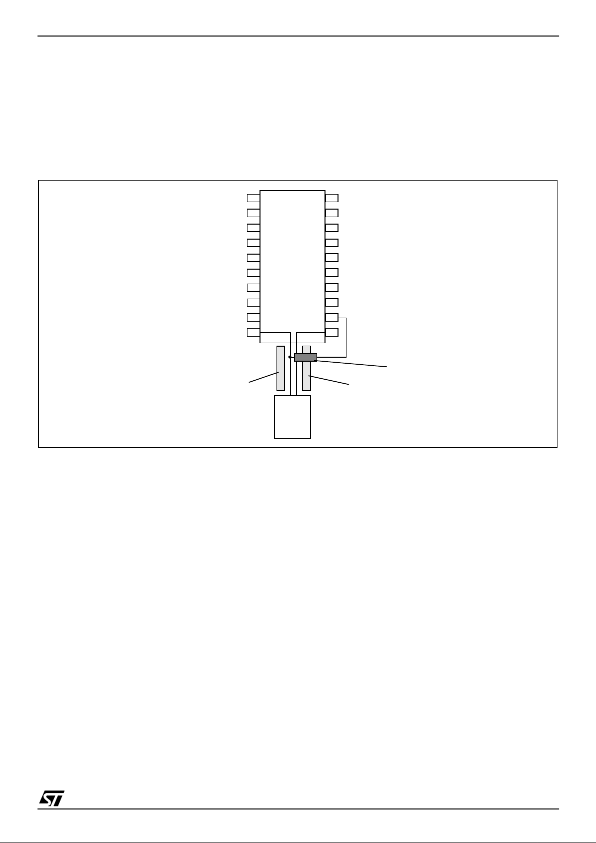
2.1 PCB LAYOUT RECOMMENDATION
In the case of DIP20 de vices the user s hould layout the PCB so that the DIP20 ST7261 device and
the USB connector are centered on the same axis
ensuring that the D- and D+ lines are of equal
len g th . Refe r to Figure 4
Figure 4. Recommended PCB Layout for USB Interface with DIP20 package
14
13
12
11
15
16
17
18
USBVCC
USBDP
1
2
3
4
5
6
7
8
9
10
19
20
USBDM
USB Connect o r
Ground
Ground
ST7261
1.5KOhm pull-up resistor
ST7261
8/80
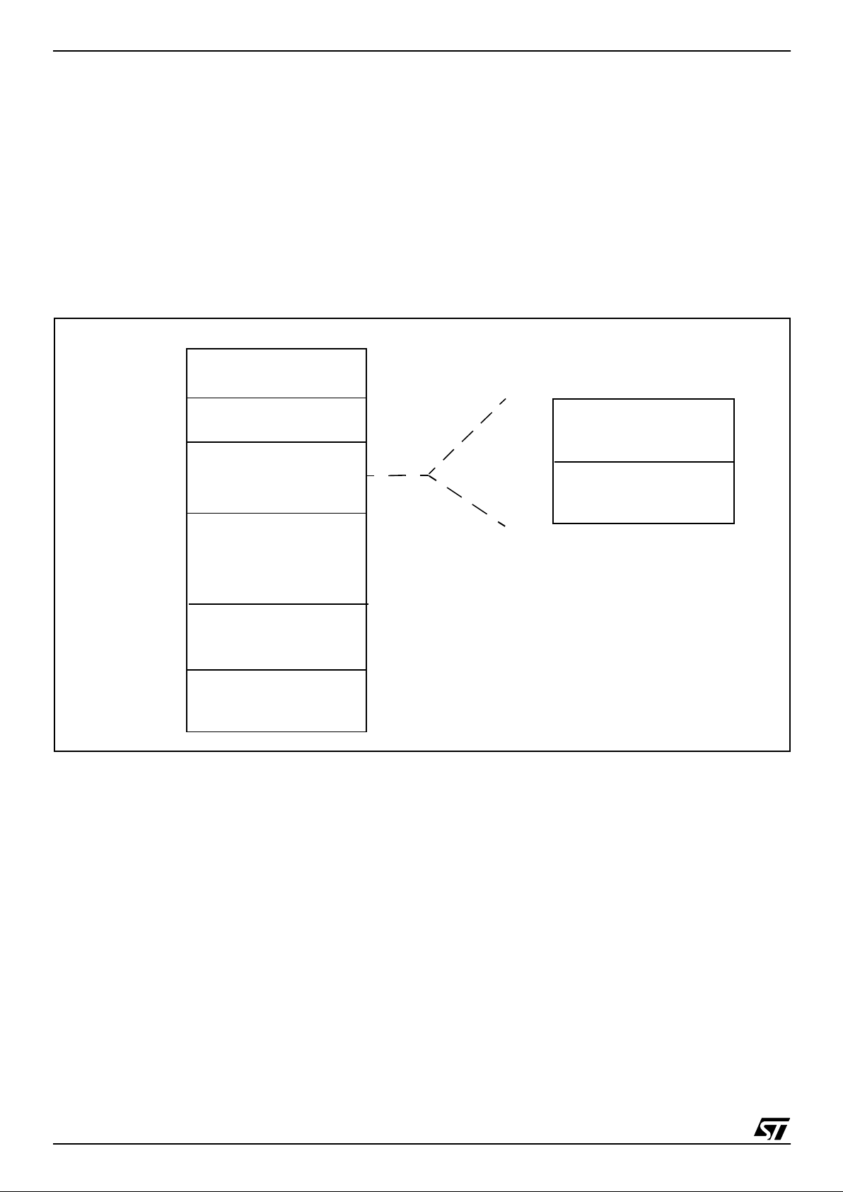
3 REGISTER & MEMORY MAP
As shown in the Figure 5, the MCU i s capable of
addressing 64K bytes of memories and I/O registers.
The available memory locations consist of 64
bytes of register locations, 256 bytes of RA M and
4 Kbytes of user program memory. The RAM
space includes up to 128 bytes for the sta ck from
0100h to 017Fh.
The highest address bytes contain the user re set
and interrupt vectors.
IMPORTANT: Memory locations marked as “Reserved” must ne ver be accessed. A ccessi ng a reseved area can have u npredict able effects on the
device.
Figure 5. Me m ory M a p
0000h
Program Memory
Interrupt & Reset Vectors
HW Registers
0040h
003Fh
(see Table 2)
FFDFh
FFE0h
FFFFh
See Table 5 on page 21
0180h
Reserved
017Fh
Short Addressing RAM
Zero page
017Fh
0080h
00FFh
(4 KBytes)
F000h
(128 Bytes)
256 Bytes RAM
Stack or
(128 Bytes)
EFFFh
16-bit Addressing RAM
Reserved
0080h
007Fh
ST7261
9/80
Table 2. Hardware Register M ap
Address Block
Register
Label
Register Name
Reset
Status
Remarks
0000h
0001h
Port A
PADR
PADDR
Port A Data Register
Port A Data Direction Register
00h
00h
R/W
R/W
0002h
0003h
Port B
PBDR
PBDDR
Port B Data Register
Port B Data Direction Register
00h
00h
R/W
R/W.
0004h
to
0007h
Reserved Area (4 Bytes)
0008h ITRFRE1 Interrupt Register 1 00h R/W
0009h MISC Miscellaneous Register 00h R/W
000Ah
to
000Ch
Reserved Area (2 Bytes)
000Dh WDG WDGCR Watchdog Control Register 7Fh R/W
000Eh to
0024h
Reserved Area (23 Bytes)
0025h
0026h
0027h
0028h
0029h
002Ah
002Bh
002Ch
002Dh
002Eh
002Fh
0030h
0031h
USB
USBPIDR
USBDMAR
USBIDR
USBISTR
USBIMR
USBCTLR
USBDADDR
USBEP0RA
USBEP0RB
USBEP1RA
USBEP1RB
USBEP2RA
USBEP2RB
USB PID Register
USB DMA Address register
USB Interrupt/DMA Register
USB Interrupt Status Register
USB Interrupt Mask Register
USB Control Register
USB Device Address Register
USB Endpoint 0 Register A
USB Endpoint 0 Register B
USB Endpoint 1 Register A
USB Endpoint 1 Register B
USB Endpoint 2 Register A
USB Endpoint 2 Register B
x0h
xxh
x0h
00h
00h
06h
00h
0000 xxxxb
80h
0000 xxxxb
0000 xxxxb
0000 xxxxb
0000 xxxxb
Read Only
R/W
R/W
R/W
R/W
R/W
R/W
R/W
R/W
R/W
R/W
R/W
R/W
0032h
to
0035h
Reserved Area (4 Bytes)
0036h
0037h
TBU
TBUCV
TBUCSR
TBU Counter Value Register
TBU Control/Status Register
00h
00h
R/W
R/W
0038h
to
003Fh
Reserved Area (8 Bytes)
ST7261
10/80
4 CENTRAL PROCE SSING UNIT
4.1 INTRODUCTION
This CPU has a full 8-bit architecture and contains
six internal registers allowing efficient 8-bit data
manipulation.
4.2 MAIN FEATURES
■ Enable executing 63 basic instructions
■ Fast 8-bit by 8-bit multiply
■ 17 main addressing modes (with indirect
addressing mode)
■ Two 8-bit index registers
■ 16-bit stack pointer
■ Low power HALT and WAIT modes
■ Priority maskable hardware interrupts
■ Non-maskable software/hardware interrupts
4.3 CPU REGISTERS
The 6 CPU registers shown in Figure 6 are not
present in the memory mapping and are accessed
by spec ifi c ins t ru c tio n s .
Accumulator (A)
The Accumulator is an 8-bit general purpose register used to hold operands and the res ults of the
arithmetic and logic calculations and to manipulate
data.
Index Registers (X and Y)
These 8-bit registers are used to create effective
addresses or as tempo rary storage areas f or data
manipulation. (The Cross -Assembler generates a
precede instruction (PRE) to indicate that the following instruction refers to the Y register.)
The Y register is not affected by the interrupt automatic procedures.
Program Counter (PC)
The program counter is a 16-bit register containing
the address of the next instruction to be executed
by the CPU. It is made of two 8-bit registers PCL
(Program Counter Low which is the LSB) and PCH
(Program Counter High which is the MSB).
Figure 6. CPU Registers
ACCUMULATOR
X INDEX REGISTER
Y INDEX REGISTER
STACK POINTER
CONDITION CODE REGISTER
PROGRAM COUNTER
70
1C1I1HI0NZ
RESET VALUE = RESET VECTOR @ FFFEh-FFFFh
70
70
70
0
7
15 8
PCH
PCL
15
8
70
RESET VALUE = STACK HIGHER ADDRESS
RESET VALUE =
1X11X1XX
RESET VALUE = XXh
RESET VALUE = XXh
RESET VALUE = XXh
X = Undefined Value
ST7261
11/80
CENTRAL PROC ESSING UNIT (Cont’d)
Condition Code Register (CC)
Read/Write
Reset Value: 111x1xxx
The 8-bit Condition Code regist er contains the i nterrupt masks and four flags representative of the
result of the instruction just executed. This register
can also be handled by the PUSH and POP instructions.
These bits can be individually tested and/or controlled by specific instructions.
Arithmetic Management Bits
Bit 4 = H
Half carry
.
This bit is set by hardware when a carry occurs between bits 3 and 4 of t he ALU during an ADD or
ADC instructions. It is reset by hardware during
the same instructio n s.
0: No half carry has occurred.
1: A half carry has occurred.
This bit is tested using the JRH or JRNH instruction. The H bit is useful in BCD arithmetic subroutine s .
Bit 2 = N
Negative
.
This bit is set and cleared by hardware. It is representative of the result sign of the last arithmetic,
logical or data manipulation. I t’s a copy of the result 7
th
bit.
0: The result of the last operation is positive or null.
1: The result of the last operation is negative
(i.e. the most significant bit is a logic 1).
This bit is accesse d by the JRMI and JRPL instructions.
Bit 1 = Z
Zero
.
This bit is set and cleared by hardware. This bit indicates that the result of the last arithmetic, logical
or data manipulation is zero.
0: The result of the last operation is different from
zero.
1: The result of the last operation is zero.
This bit is accessed by the JREQ and JRNE test
instructions.
Bit 0 = C
Carry/borrow.
This bit is set and cleared b y hardware and software. It indicates an overflow or an un derflow has
occurred during the last arithmetic operation.
0: No overflow or underflow has occurred.
1: An overflow or underflow has occurred.
This bit is driven by the SCF and RCF instructions
and tested by the JRC and JRNC instructions. It i s
also affected by the “bit test and branch”, shift and
rotate instructions.
Interrupt Managem e nt B i ts
Bit 5,3 = I1, I0
Interrupt
The combination of the I1 and I0 bits gives the current interrupt software priority.
These two bits are set/cleared by hardware when
entering in interrupt. The loaded value is given by
the corresponding bits in the interrupt software priority registers (IxSPR). They can be also set/
cleared by software with the RIM, SIM, IRET,
HALT, WFI and PUSH/POP instructions.
See the interrupt management chapter for more
details.
70
11I1HI0NZ
C
Interrupt Software Priorit y I1 I0
Level 0 (main) 1 0
Level 1 0 1
Level 2 0 0
Level 3 (= interrupt disable) 1 1
ST7261
12/80
CPU REGISTERS (Cont’d)
STACK POINTER (SP)
Read/Write
Reset Value: 017Fh
The Stack Pointer is a 16-bit register which is always pointing to the next free location in the stack.
It is then decremented after data has been pushed
onto the stack and incremented before data is
popped from the stack (see Figure 7).
Since the stack is 128 bytes deep, the 9 most significant bits are forced by hard ware. Following a n
MCU Reset, or after a Reset Stack Pointer instruction (RSP), the Stack Pointer contains its reset value (the SP6 to SP0 bits are set) which is the stack
higher address.
The least significant byte of the Stack Pointer
(called S) can be directly accessed by a LD instruction.
Note: When the lower limit is exceeded, the Stack
Pointer wraps around to the stack upper limit, without indicating the stack overflow. The previously
stored information is then o verwritten and therefore lost. The stack also wraps in case of an underflow.
The stack is used to sav e the return address during a subroutine call and the CPU context during
an interrupt. The user may also directly manipulate
the stack by means of the PUSH and POP instructions. In the case of an interrupt, the PCL is stored
at the first location po inted t o by t he SP. Th en t he
other registers are stored in the next locations as
shown in Figure 7.
– When an interrupt is received, the SP is decre-
mented and the context is pushed on the stack.
– On return from interrupt, the SP is incremented
and the context is popped from the stack.
A subroutine call occupies two locations and an interrupt five locat ion s i n the stack ar ea.
Figure 7. Stack Manipulation Example
15 8
00000001
70
1 SP6 SP5 SP4 SP3 SP2 SP1 SP0
PCH
PCL
SP
PCH
PCL
SP
PCL
PCH
X
A
CC
PCH
PCL
SP
PCL
PCH
X
A
CC
PCH
PCL
SP
PCL
PCH
X
A
CC
PCH
PCL
SP
SP
Y
CALL
Subroutine
Interrupt
Event
PUSH Y POP Y IRET
RET
or RSP
@ 017Fh
@ 0100h
Stack Higher Address = 017Fh
Stack Lower Address =
0100h
ST7261
13/80
5 CLOCKS AND RESET
5.1 CLOCK SYSTEM
5.1.1 General Description
The MCU accepts either a Crystal or Ceramic resonator, or an external clock signal to drive the internal oscillator. The internal clock (f
CPU
) is de-
rived from the external oscillator frequency (f
OSC
),
by dividing by 3 and multiplying by 2. By setting the
OSC12/6 bit in the option byte, a 12 MHz ex ternal
clock can be used giving an internal frequency of 8
MHz while maintaining a 6 MHz clock for USB (refer to Figure 10).
The internal clock signal (f
CPU
) consists of a
square wave with a duty cycle of 50%.
It is further divided by 1, 2, 4 or 8 depending on the
Slow Mode Selection bits in the Miscellaneous
register ( SMS[1:0 ])
The internal oscillat or is designed to operate with
an AT-cut parallel resonant quartz or ceramic resonator in the frequency range specified for f
osc
.
The circuit shown in Figure 9 is recommended
when using a crystal, and Table 3 lists the recommended capacitors. The crystal and associated
components shoul d be m ounted as close as possible to the input pins in order to minimize output
distortion and start-up stabilization time.
Table 3. Recommended Values for 12 MHz
Crystal Resonator
Note: R
SMAX
is the equivalent serial resistor of the
crystal (see crystal specification).
5.1.2 External Clock input
An external clock may be applied to the OSCIN input with the OSCOUT pin not connected, as
shown on F igure 8. The t
OXOV
specifications does
not apply when using an external clock input. The
equivalent specification of the external clock
source should be used instead of t
OXOV
(see Elec-
tr ical C haracteristic s).
5.1.3 Clock Output Pin (MCO)
The internal clock (f
CPU
) can be output on Port B0
by setting the MCO bit in the Misce llaneous register.
Figure 8. External Clock Source Connections
Figure 9. Crystal/Ceramic Resonator
Figure 10. Clock block diagram
R
SMAX
20
Ω
25
Ω
70
Ω
C
OSCIN
56pF 47pF 22pF
C
OSCOUT
56pF 47pF 22pF
R
P
1-10 M
Ω
1-10 M
Ω
1-10 M
Ω
OSCIN OSCOUT
EXTERNAL
CLOCK
NC
OSCIN
OSCOUT
C
OSCIN
C
OSCOUT
to CPU and
f
CPU
8/4/2/1 MHz
6 MHz (USB)
12 or
peripherals
%2
0
1
OSC12/6
6 MHz
Crystal
x2
Slow
Mode
%
SMS[1:0]
1/2/4/8
%3
(or 4/2/1/0.5 MHz)
MCO pin
ST7261
14/80
5.2 RESET
The Reset procedure is used to provide an orderly
software start-up or to exit low power modes.
Three reset modes are provided: a low voltage reset, a watchdog reset and an ext ernal reset at the
RESET
pin.
A reset causes the reset vector to be fetched from
addresses FFFEh and FFFFh in order to be loaded
into the PC and with program execution starting
from this point.
An internal circuitry provides a 5 14 CPU clock cycle delay from the time that the oscillator becomes
active.
5.2.1 Low Voltage Reset
Low voltage reset circuitry generates a reset when
V
DD
is:
■ below V
IT+
when VDD is rising,
■ below V
IT-
when VDD is falling.
During low voltage reset, the RESET
pin is held low,
thus permitting the MCU to reset other devices.
The Low Voltage Detector can be disabled by setting the LVD bit of the Option byte.
5.2.2 Watchdog Reset
When a watchdo g reset occ urs, t he RESET
pin is
pulled low permitting the MCU to reset other devices as when low voltage reset (Figur e 11).
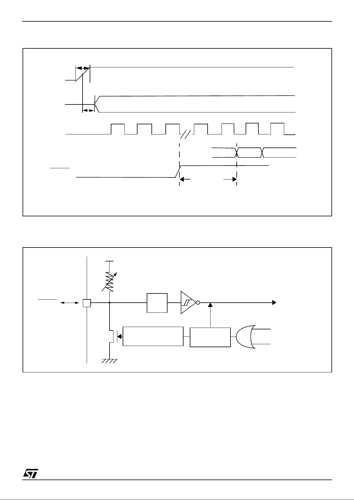
5.2.3 External Reset
The external reset is an active low input signal applied to the RESET
pin of the MCU.
As shown in Figure 14, the RESET
signal must
stay low for a minimum of one and a half CPU
clock cycles.
An internal Schmitt trigger at the RESET
pin is pro-
vided to improve noise immunity.
Figure 11. Low Voltage Reset functional Diagram
Figure 12. Low Voltage Reset Signal Output
Note: Typical hysteresis (V
IT+-VIT-
) of 250 mV is
expected
Figure 13. Temporization Timing Diagram after an internal Reset
LOW VOLTAGE
V
DD
FROM
WATCHDOG
RESET
RESET
INTERNAL
RESET
RESET
RESET
V
DD
V
IT+
V
IT-
V
DD
Addresses
$FFFE
Temporization
V
IT+
(514 CPU clock cycles)
ST7261
15/80
Figure 14. Reset Timing Diagra m
Note: Refer to Electrical Characteristics for values of t
DDR
, t
OXOV
, V
IT+
and V
IT-.
Figure 15. Reset Block Diagram
Note: The output of the external reset circuit must have an open-drain output to drive the ST7 reset pad.
Otherwise the device can be damaged when the ST7 generates an internal reset (LVD or watchdog).
V
DD
OSCIN
f
CPU
FFFF
FFFE
PC
RESET
t
DDR
t
OXOV
514 CPU
CLOCK
CYCLES
DELAY
RESET
R
ON
V
DD
WATCHDOG RESET
LVD RESET
INTERNAL
RESET
PULSE
GENERATOR
200ns
Filter
t
w(RSTL)out
+ 128 f
OSC
delay
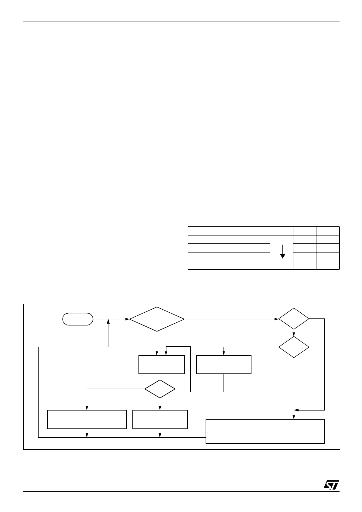
ST7261
16/80
6 INTERRUP T S
6.1 INTRODUCTION
The CPU enhanced interrupt management provides the following features:
■ Hardware interrupts
■ Software interrupt (TRAP)
■ Nested or concurrent interrupt management
with flexible interrupt priority and level
management:
– Up to 4 software programmable nesting levels
– Up to 16 interrupt vectors fixed by hardware
– 3 non maskable events: RESET, TRAP, TLI
This interrupt management is based on:
– Bit 5 and bit 3 of the CPU CC register (I1:0),
– Interrupt software priority registers (ISPRx),
– F ixed interrupt vecto r addresses locat ed at the
high addresses of the memory map (FFE0h to
FFFFh) sorted by hardware priority order.
This enhanced interrupt cont roller guarantees full
upward compatibility with the standard (not nested) CPU interrupt controller.
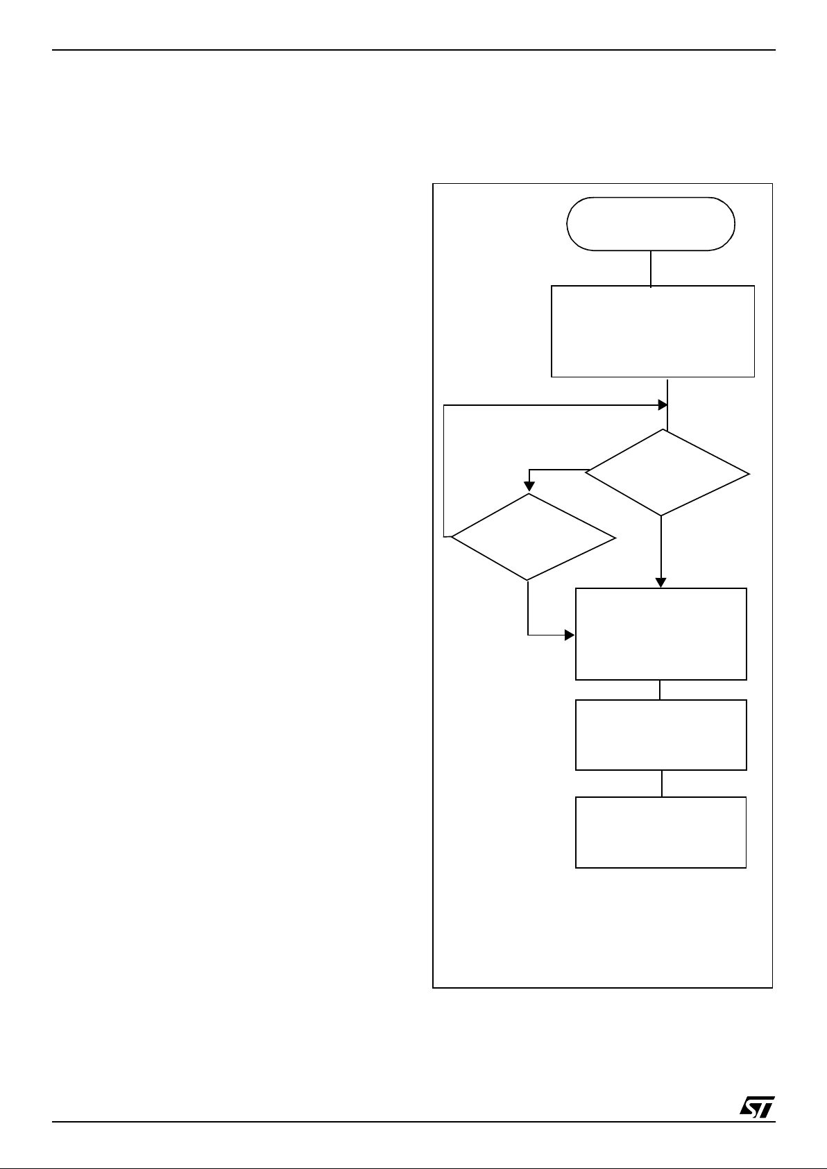
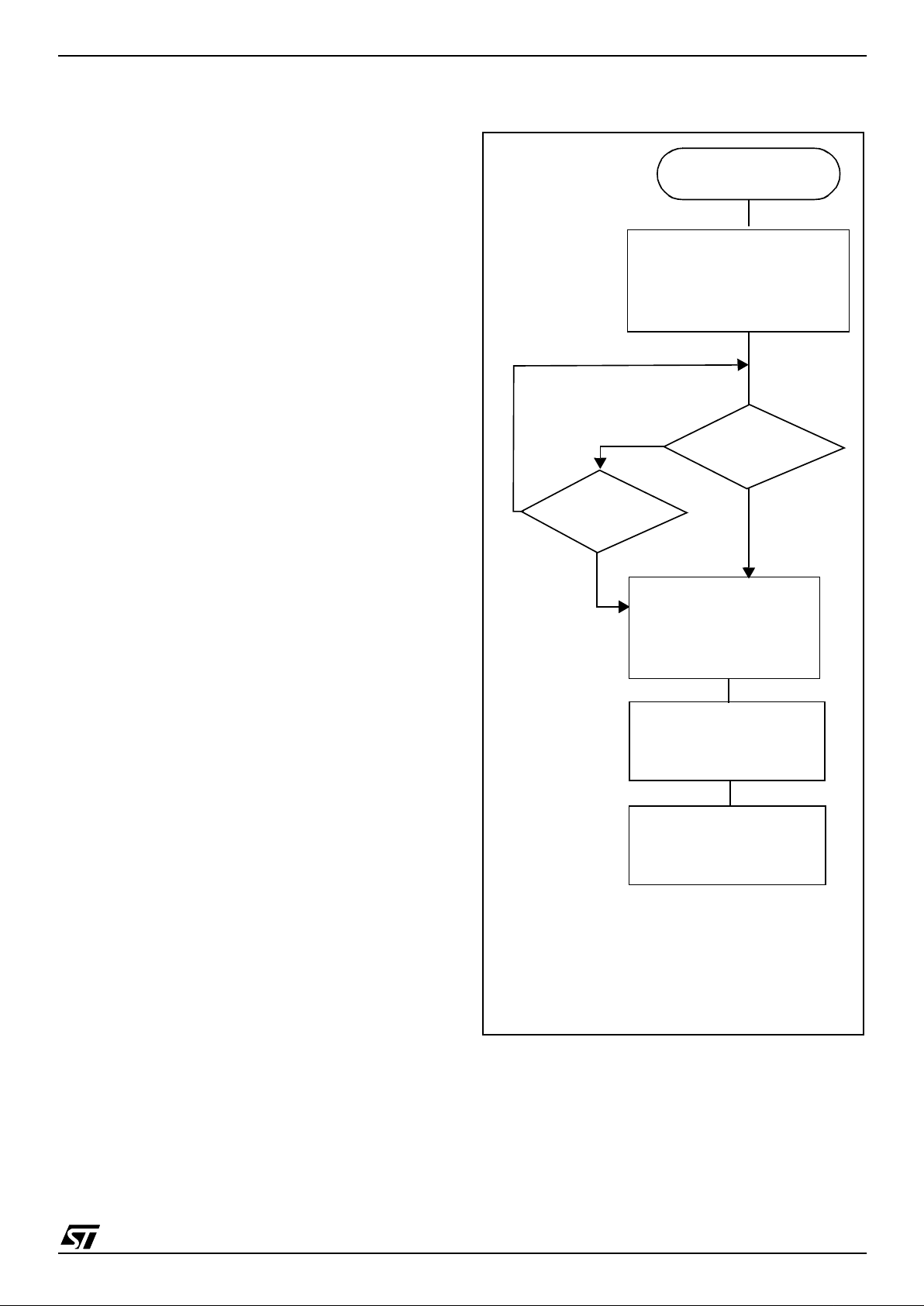
6.2 MASKI N G AND PRO C ESSING FLOW
The interrupt masking is managed by the I1 and I0
bits of the CC register and the ISPRx registers
which give the interrupt software priority level of
each interrupt vector (see Table 4 ). The processing flow is shown in Fi gure 16.
When an interrupt request has to be serviced:
– Normal processing is suspended at the end of
the current instruction execution.
– The PC, X, A and CC registers are saved onto
the stack.
– I1 and I0 bits of CC register are set according to
the corresponding values in the ISPRx registers
of the serviced interrupt vector.
– The PC is then loaded with the interrupt vector of
the interrupt to service and the first instruction of
the interrupt service routine is fetched (refer to
“Interrupt Mapping” table for vector addresses).
The interrupt service routine should end with the
IRET instruction which c auses the contents of t he
saved registers to be recovered from the stack.
Note: As a consequence of the IRET instruction,
the I1 and I0 bits will be restored from the stack
and the program in the previous level will resume.
Table 4. Interrupt Software Priority Levels
Figure 16. Int errupt Processing Flowchart
Interrupt software priority Level I1 I0
Level 0 (main) Low
High
10
Level 1 0 1
Level 2 0 0
Level 3 (= interrupt disable) 1 1
“IRET”
RESTORE PC, X, A, CC
STACK PC, X, A, CC
LOAD I1:0 FRO M INTER RUPT SW REG.
FETCH NEX T
RESET
TLI
PENDING
INSTRUCTION
I1:0
FROM STACK
LOAD PC FROM INTERRUPT VECTOR
Y
N
Y
N
Y
N
Interrupt has the same or a
lower software priority
THE INTERRUPT
STAYS PENDING
than c u rrent on e
Interrupt has a higher
softwarepriori ty
than current one
EXECUTE
INSTRUCTION
INTERRUPT
ST7261
17/80
INTERRUPTS (Cont’d)
Servicing Pending In te rrupts
As several interrupts can b e pen ding at the s ame
time, the interrupt to be taken into account is determined by the following two-step process:
– the highest software priority interrupt is serviced,
– i f several interrupts have the same software pri-
ority then the interrupt with the highest hardware
priority is serviced first.
Figure 17 describes this decision process.
Figure 17. Priority Decision Process
When an interrupt request is not serviced immediately, it is latched and then processed when its
software priority combined with the hardware priority becomes the highest one.
Note 1: The hardware priority is exclusive while
the software one i s not. This allows the prev ious
process to succeed with only one interrupt.
Note 2: RESET, TRAP and TLI can be considered
as having the highest softwa re priority in the d ecision process.
Different Interrupt Vector Sources
Two interrupt source types are managed by the
CPU interrupt controller: the non-maskable type
(RESET, TLI, TRAP) and the maskable type (external or from internal peripherals).
Non-Maskable Sources
These sources are processed regardless of the
state of the I1 and I0 bits of the CC register (see
Figure 16). After stacking the PC, X, A and CC
registers (except for RESET), the corresponding
vector is loaded in the PC register and t he I1 and
I0 bits of the CC are set to disable interrupts (level
3). These sources allow the processor to exit
HALT mode.
■ TLI (Top Level Hardware Interrupt)
This hardware interrupt occurs when a specific
edge is detected on the dedicated TLI pin.
Caution: A TRAP instruction must not be used in a
TLI serv i ce routine.
■ TRAP (Non Maskable Software Interrupt)
This software interrupt is serviced when the TRAP
instruction is executed. It will be serviced according to the flowchart in Figure 16 as a TLI.
Caution: TRAP can be interrupted by a TLI.
■ RESET
The RESET source has the highest priority in the
CPU. This means that the first current routine has
the highest software priority (level 3) and the highest hardware priority.
See the RESET chapter for more details.
Maskable Sources
Maskable interrup t vector sourc es can be servi ced
if the corresponding in terrupt is enabled and if its
own interrupt software priority (in ISPRx registers)
is higher than the one currently being serviced (I1
and I0 in CC register). If any of these two co nditions is false, the interrupt is la tched and thus remains pending.
■ External Interrupts
External interrupts allow the processor to exit from
HALT low power mode.
External interrupt sensitivity is software selectable
through the ITRFRE2 register.
External interrupt triggered on edge will be latched
and the interrupt request automatically cleared
upon entering the interrupt service routine.
If several input pins of a group connected to the
same interrupt line are selected simultaneously,
these w ill be log i cally NANDed.
■ Peripheral Interrupts
Usually the peripheral interrupts cause the Device
to exit from HALT mode except those mentioned in
the “Interrupt Mapping” table.
A peripheral interrupt occurs when a specific flag
is set in the peripheral status registers and if the
corresponding enable bit is set in the peripheral
control register.
The general sequence for clearing an interrupt is
based on an access to the status register followed
by a read or write to an associated register.
Note: The clearing sequence resets the internal
latch. A pending interrupt (i.e. waiting for being
serviced) will therefore be lost if the clear sequence is executed.
PENDING
SOFTWARE
Different
INTERRUPTS
Same
HIGHEST HARDWARE
PRIORITY SERVICED
PRIORITY
HIGHEST SOFTWARE
PRIORITY SERVICED
ST7261
18/80
INTERRUPTS (Cont’d)
6.3 INTERRUPTS AND LOW POWER MODES
All interrupts allow the processor to exit the WAIT
low power mode. On the contrary, only external
and other specified interrupt s allow the processor
to exit from the HALT modes (see column “Exit
from HALT” in “Interrupt Mapping” table). When
several pending interrupts are present whi le exiting HALT mode, the first one serviced can only be
an interrupt with e xit from HALT mode c apability
and it is selected through the same decision proc ess shown in Figure 17.
Note: If an interrupt, that is not able to Exit from
HALT mode, is pending with the highest priority
when exiting HALT mode, this interrupt is serviced
after the first one serviced.
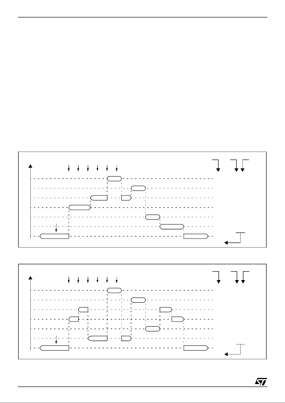
6.4 CONCURRENT & NESTED MANAGEMENT
The following Figure 18 and Figure 19 show two
different interrupt management modes. The first is
called concurrent mode and do es not allow an interrupt to be interrupted, unlike the nested mode in
Figure 19. The interrupt hardware priority is given
in this order from the l owes t to the hi ghest: M A IN,
IT4, IT3, IT2, IT1, IT0, TLI. The software priority is
given for each interrupt.
Warning: A stack overflow may occur without notifying the software of the failure.
Figure 18. Concurrent Interru pt Manage m ent
Figure 19. Nested Interrupt Management
MAIN
IT4
IT2
IT1
TLI
IT1
MAIN
IT0
I1
HARDWARE PRIORITY
SOFTWARE
3
3
3
3
3
3/0
3
11
11
11
11
11
11 / 10
11
RIM
IT2
IT1
IT4
TLI
IT3
IT0
IT3
I0
10
PRIORITY
LEVEL
USED STACK = 10 BYTES
MAIN
IT2
TLI
MAIN
IT0
IT2
IT1
IT4
TLI
IT3
IT0
HARDWARE PRIORITY
3
2
1
3
3
3/0
3
11
00
01
11
11
11
RIM
IT1
IT4
IT4
IT1
IT2
IT3
I1 I0
11 / 10
10
SOFTWARE
PRIORITY
LEVEL
USED STACK = 20 BYTES
ST7261
19/80
INTERRUPTS (Cont’d)
6.5 INTERRUPT REGISTER DESCRIPTION
CPU CC REGISTER INTERRUPT BITS
Read/Write
Reset Value: 111x 1010 (xAh)
Bit 5, 3 = I1, I0
Soft w a re In te r rupt Prio rity
These two bits indicate the current interrupt software priority.
These two bits are set/cle ared by hardware whe n
entering in interrupt. The loaded value is given by
the corresponding bits in the interrupt software priority registers (ISPRx).
They can be also s et/cleared by s oft ware wi th the
RIM, SIM, HALT, WFI, IRET and PUSH/POP instructions (see “Interrupt Dedicated Instruction
Set” table).
*Note: TLI, TRAP and RESET events ca n in terru pt
a level 3 program.
INTERRUPT SOFTWARE PRIORITY REGISTERS (ISPRX)
Read/Write (bit 7:4 of ISPR3 are read only)
Reset Value: 1111 1111 (FFh)
These four registers contain the interrupt software
priority of each interrupt vector.
– Each interrupt vector (except RESET and TRAP)
has corresponding bits in these registers where
its own software priority is stored. This correspondance is shown in the following table.
– Each I1_x and I0_x bit value in the ISPRx regis-
ters has the same meaning as the I1 and I0 bits
in the CC register.
– Level 0 can not be written (I1_x=1, I0_x=0). In
this case, the previously stored value is kept. (example: previous=CFh, write=64h, result=44h)
The RESET, TRAP a nd TLI vectors have no s oftware priorities. When one is serviced, the I1 and I0
bits of the CC register are both set.
*Note: Bits in the ISPRx registers which correspond to the TLI can be read and written but they
are not significant in the interrupt process management.
Caution: If the I1_x and I0_x bits are modified
while the interrupt x is execu ted the following behaviour has to be considered: If the interrupt x is
still pending (new interrupt or flag not cleared) and
the new software priority is highe r than the previous one, the interrupt x is re-ent ered. Otherwise,
the software priority stays unchanged up to the
next interrupt request (after the IRET of the interrupt x).
70
11I1 H I0 NZC
Interrupt Software Priority Level I1 I0
Level 0 (main)
Low
High
10
Level 1 0 1
Level 2 0 0
Level 3 (= interrupt disable*) 1 1
70
ISPR0 I1_3 I0_3 I1_2 I0_2 I1_1 I0_1 I1_0 I0_0
ISPR1 I1_7 I0_7 I1_6 I0_6 I1_5 I0_5 I1_4 I0_4
ISPR2 I1_11 I0_11 I1_10 I0_10 I1_9 I0_9 I1_8 I0_8
ISPR3 1 1 1 1 I1_13 I0_13 I1_12 I0_12
Vector address ISPRx bits
FFFBh-FFFAh I1_0 and I0_0 bits*
FFF9h-FFF8h I1_1 and I0_1 bits
... ...
FFE1h-FFE0h I1_13 and I0_13 bits
ST7261
20/80
6.6 Interrupt Register
INTERRUPT REGISTER 1 (ITRFRE1)
Address: 0008h - Read/Write
Reset Value: 0000 0000 (00h)
Bit 7:0 = ITiE
Interrupt Enable
0: I/O pin free for general purpose I/O
1: ITi external interrupt enabled.
Note: The corresponding interrupt is generated
when:
– a rising edge occurs on the IT5/IT6 pins
– a falling edge occurs on the IT1, 2, 3, 4, 7 and 8
pins
INTERRUPT REGISTER 2 (ITRFRE2)
Address: 0039h - Read/Write
Reset Value: 0000 0000 (00h)
Bit 7:6 = CTL[3:2]
IT[12:11] Interrupt Sensitivity
These bits are set and cleared by software. They
are used to configure the edge and level sensitivity
of the IT12 and IT11 external interrupt pins (this
means that both must have the same sensitivity).
Bit 5:4 = CTL[1:0]
IT[10:9]1nterrupt Sensitivity
These bits are set and cleared by software. They
are used to configure the edge and level sensitivity
of the IT10 and IT9 external interrupt pins (this
means that both must have the same sensitivity).
Bit 3:0 = ITiE
Interrupt Enable
0: I/O pin free for general purpose I/O
1: ITi external interrupt enabled.
70
IT8E IT7E IT 6E IT5E IT4E IT3E IT2E IT1E
70
CTL3 CTL2 CTL1 CTL0 IT12E IT11E IT10E IT9E
CTL3 CTL2 IT[12:11] Sensitivity
0 0 Falling edge and low level
0 1 Rising edge only
1 0 Falling edge only
1 1 Rising and falling edge
CTL1 CTL0 IT[10:9] Sensitivity
0 0 Falling edge and low level
0 1 Rising edge only
1 0 Falling edge only
1 1 Rising and falling edge
ST7261
21/80
INTERRUPTS (Cont’d)
Table 5. I nte rrupt Mapping
Table 6. Nested Interrupts Register Map and Reset Values
N°
Source
Block
Description
Register
Label
Exit
from
HALT
Address
Vector
Priority
Order
Reset Vector Yes FFFEh-FFFFh
Highest
Priority
Lowest
Priority
TRAP software interrupt vector No FFFCh-FFFDh
0 NOT USED FFFAh-FFFBh
1 USB USB End Suspend interrupt vector USBISTR Yes FFF8h-FFF9h
2
I/O Ports
Port A external interrupts IT[3:1]
ITRFRE1
Yes FFF6h-FFF7h
3 Port B external interrupts IT[8:5] Yes FFF4h-FFF5h
4 NOT USED FFF2h-FFF3h
5 TBU Timebase Unit interrupt vector TBUCSR No FFF0h-FFF1h
6 NOT USED FFEEh-FFEFh
7 NOT USED FFECh-FFEDh
8 NOT USED FFEAh-FFEBh
9 USB USB interrupt vector USBISTR No FFE8h-FFE9h
10 NOT USED FFE6h-FFE7h
Address
(Hex.)
Register
Label
76543210
0032h
ISPR0
Reset Value
Ext. Interrupt Port B Ext. Interrupt Port A USB END SUSP Not Used
I1_3
1
I0_3
1
I1_2
1
I0_2
1
I1_1
1
I0_1
111
0033h
ISPR1
Reset Value
SPI ART TBU Ext. Interrupt Port C
I1_7
1
I0_7
1
I1_6
1
I0_6
1
I1_5
1
I0_5
1
I1_4
1
I0_4
1
0034h
ISPR2
Reset Value
Not Used ADC USB SCI
I1_11
1
I0_11
1
I1_10
1
I0_10
1
I1_9
1
I0_9
1
I1_8
1
I0_8
1
0035h
ISPR3
Reset Value1111
Not Used Not Used
I1_13
1
I0_13
1
I1_12
1
I0_12
1
ST7261
22/80
7 POWER SAVING MODES
7.1 INTRODUCTION
There are three Power Saving modes. Slow Mode
is selected by setting the SMS bits in the Miscellaneous register. Wait and Halt modes may be entered using the WFI and HALT instructions.
After a RESET the normal operating mode is selected by default (RUN mode). This mode drives
the device (CPU and embedded peripherals) by
means of a master clock which is based on the
main oscillator f requency divide d by 3 and multiplied by 2 (f
CPU
).
From Run mode, the different power saving
modes may be selected by setting the relevant
register bits or by calling the specific ST7 software
instruction whose action depends on the oscillator
status.
7.1.1 Slow Mode
In Slow mode, the osc illator frequency can be d ivided by a value defined in the Miscellaneous
Register. The CPU and peripherals are clocked at
this lower frequency. Slow mode is used to reduce
power consumption, and enables the user to adapt
clock frequency to available supply voltage.
7.2 WAIT MODE
WAIT mode places the MCU in a low power c onsumption mode by stopping the CPU.
This pow e r s a v ing mo de is se lected b y ca llin g the
“WFI” ST7 software instruction.
All peripherals remain active. During WAIT mode,
the I bit of the CC register is forced to 0, to enable
all interrupts. All other registers and memory remain unchanged. The MCU remains in WAIT
mode until an interrupt or Res et oc curs, where upon the Program Counter branches to the starting
address of the interrupt or Reset service routine.
The MCU w ill re mai n in W AIT mo de unt il a Res et
or an Interrupt occurs, causing it to wake up.
Refer to Figure 20.
Figure 20. WAIT Mode Flow Chart
WFI INSTRUCTION
RESET
INTERRUPT
Y
N
N
Y
CPU CLOCK
OSCILLATOR
PERIPH. CLOCK
I-BIT
ON
ON
CLEARED
OFF
CPU CLOCK
OSCILLATOR
PERIPH. CLOCK
I-BIT
ON
ON
SET
ON
FETCH RESET VECTOR
OR SERVICE INTERRUPT
514 CPU CLOCK
CYCLES DELAY
IF RESET
Note: Before servicing an interrupt, the CC register is
pushed on the sta ck. The I-Bit is s et d uring the inte rrupt routine and cleared when the CC register is
popped.
ST7261
23/80
POWER SAVING MODES (Cont’d)
7.3 HALT MODE
The HALT mode is the MCU lowest power consumption mode. The HALT mode is entered by executing the HALT instruction. The internal oscillator is then turned off, causing all internal processing to be stopped, including the operation of the
on-chip peripherals.
When entering HALT mode, the I bit in the Condition Code Register is cleared. Thus, any of the external interrupts (ITi or US B end suspend mode),
are allowed and if an interrupt occurs, the CPU
clock becomes active.
The MCU can e xit HAL T mode on reception of either an external interrupt on ITi, an end suspen d
mode interrupt coming from USB peripheral, or a
reset. The osc illato r is t hen t ur ned on and a stabilization time is provided before rele as ing CPU operation. The stabilization time is 514 CPU clock cycles.
After the start up delay, the CPU continues operation by servicing the interrupt which wakes it up or
by fetching the reset vector if a reset wakes it up.
Figure 21. HALT Mod e Flo w C ha r t
N
N
EXTERNAL
INTERRUPT*
RESET
HALT INSTRUCTION
514 CPU CLOCK
FETCH RESET VECTOR
OR SERVICE INTERRUPT
CYCLES DELAY
CPU CLOCK
OSCILLATOR
PERIPH. CLOCK
I-BIT
ON
ON
SET
ON
CPU CLOCK
OSCILLATOR
PERIPH. CLOCK
I-BIT
OFF
OFF
CLEARED
OFF
Y
Y
Note: Before servicing an interrupt, the CC register is
pushed on the stac k. T he I -Bit i s se t du ring the interrupt routine and cleared when the CC register is
popped.
ST7261
24/80
8 I/O PORTS
8.1 INTRODUCTION
The I/O ports offer different functional modes:
transfer of data through digital inputs and outputs
and for specific pins:
– Analog signal input (ADC)
– Alternate signal input/out put for the on-chip pe-
ripherals.
– External interrupt generation
An I/O port i s c om posed of up to 8 pins. Each pi n
can be programmed independently as digital input
or digital output.
8.2 FUNCTIONAL DESCRIPTION
Each port is associated with 2 main registers:
– Data Register (DR)
– Data Direction Register (DDR)
Each I/O pin may be programmed using the corre-
sponding register bits in DDR regi ster: bi t x corresponding to pin x of the port. The same correspondence is used for the DR register.
Table 7. I /O Pi n Fu nc ti ons
8.2.1 Input Modes
The input configuration is s ele cted by clearing the
corresponding DDR register bit.
In this case, reading the DR register returns the
digital value applied to the external I/O pin.
Notes:
1. All the inputs are triggered by a Schmitt trigger.
2. When switching from input mode to output
mode, the DR reg ister should be writte n first to
output the correct value as s oon as the port is
configured as an output.
Interrupt function
When an external interrupt function of an I/O pin, is
enabled using the ITFRE registers, an event on
this I/O can generate an external Interrupt request
to the CPU. The i nterrupt sensitivit y is programma-
ble, the options are given in the description of the
ITRFRE interrupt registers.
Each pin can independently generate an I nterrupt
request.
Each external interrupt vecto r is linked to a dedicated group of I/O port pins (see Interrupts section). If more than one input pin is selected sim ultaneously as interrupt source, this is logically ANDed and inverted. For this reason, if an event occurs on one of the i nterrupt pins, it masks t he other
ones.
8.2.2 Output Mode
The pin is configured in output mode by setting the
corresponding DDR register bit (see Table 7).
In this mode, writing “0” or “1” to the DR register
applies this digital value to the I/O pin through the
latch. Then reading the DR register returns the
previously stored value.
Note: In this mode, the interrupt function is disabled.
8.2.3 Alternate Functions
Digital A lternate Fu nct i on s
When an on-chip peripheral is configured to use a
pin, the alternate function is au tomatically selected. This alternate function takes priority over
standard I/O programming. When the signal is
coming from an on-chip peripheral, the I/O pin is
automatically configured in output mode (push-pull
or open drain according to the peripheral).
When the signal is goi ng t o an on-c hip pe ripheral,
the I/O pin ha s to be configured in input m ode. In
this case, the pin state is also digitally readable by
addressing the DR register.
Notes:
1. Input pull-up conf iguration can cause a n unexpected value at the alternate peripheral input.
2. When the on-chip peripheral uses a pin as input
and output, this pin must be configured as an
input (DDR = 0).
Warning
: Alternate functions of peripherals must
must not be activated when the external interrupts
are enabled on the same pin, in order to avoid
generating spurious interrupts.
DDR MODE
0 Input
1 Output

ST7261
25/80
I/O PORTS (Cont’d)
Analog Alternate Functions
When the pin is used as an ADC input, the I/O
must be configured as input. The analog multiplexer (controlled by the ADC regi sters) switches the
analog voltage present o n the selected pin to th e
common analog rail which is connected to the
ADC input.
It is recommended not to change the voltage level
or loading on any port pin while conversion is in
progress. Furthermore it is recommended not to
have clocking pins located c lose to a selected analog pin.
Warning
: The analog input voltage level must be
within the limits s tated in the A bsolute Ma ximum
Ratings.
8.2.4 I/O Port Implementation
The hardware implementation on each I/O port depends on the settings in the DDR register and specific features of the I/O port such as ADC Input or
true open drain.

ST7261
26/80
I/O PORTS (Cont’d)
8.2.5 Port A
Table 8. Port A Description
Figure 22. PA[2:0] Configuration
PORT A
I/O Alternate Function
Input* Output Signal Condition
PA0 floating push-pull
USBOE USBOE = 1 (MISC)
IT1 Schmitt triggered input IT1E = 1 (ITRFRE1)
PA1 floating push-pull IT2 Schmitt triggered input IT2E = 1 (ITRFRE1)
PA2 floating push-pull IT3 Schmitt triggered input IT3E = 1 (ITRFRE1)
*Reset State
DR
DDR
LATCH
LATCH
DR SEL
DDR SEL
V
DD
PAD
ALTERNATE ENABLE
ALTERNATE ENABLE
DIGITA L EN AB L E
ALTE RN AT E ENABL E
ALTER NAT E
ALTERN AT E INPUT
OUTPUT
P-BUFFER
N-BU FF E R
1
0
1
0
V
SS
DATA BUS
V
DD
DIODES

ST7261
27/80
I/O PORTS (Cont’d)
8.2.6 Port B
Table 9. Port B Description
Figure 23. Port B Conf i gu ra ti on
PORT B
I/O Alternate Function
Input* Output Signal Condition
PB0 floating push-pull (high sink) MCO (Main Clock Output) MCO = 1 (MISCR)
PB1 floating push-pull (high sink)
PB2 floating push-pull (high sink)
PB3 floating push-pull (high sink)
PB4 floating push-pull (high sink) IT5 Schmitt triggered input IT5E = 1 (ITRFRE1)
PB5 floating push-pull (high sink) IT6 Schmitt triggered input IT6E = 1 (ITRFRE1)
PB6 floating push-pull (high sink) IT7 Schmitt triggered input IT7E = 1 (ITRFRE1)
PB7 floating push-pull (high sink) IT8 Schmitt triggered input IT8E = 1 (ITRFRE1)
*Reset State
DR
DDR
LATCH
LATCH
DR SEL
DDR SEL
V
DD
PAD
ALTERNATE ENABLE
ALTERNATE ENABLE
ALTERNATE ENABLE
ALTERNATE
ALTERNATE INPUT
OUTPUT
P-BUFFER
N-BUFFER
1
0
1
0
CMOS SCHMITT TRIGGER
V
SS
V
DD
DIODES
DATA BUS

ST7261
28/80
I/O P O R TS (Cont’d)
8.2.7 Register Description
DATA REGISTER (DR)
Port x Data Register
PxDR with x = A or B.
Read/Write
Reset Value: 0000 0000 (00h)
Bit 7:0 = D[7:0]
Data register 8 bits.
The DR register has a specific behaviour according to the selected input/output configuration. Writing the DR register is always taken into account
even if the pin is configured as an input; this allows
to always have the expected level on the pin when
toggling to output mode. Reading the DR register
returns either the DR register latch content (pin
configured as output) or the digital value applied to
th e I /O pin (pi n configured as input).
DATA DIRECTION REGISTER (DDR)
Port x Data Direction Register
PxDDR with x = A or B.
Read/Write
Reset Value: 0000 0000 (00h)
Bit 7:0 = DD[7:0]
Data direction register 8 bits.
The DDR reg ister gives the i nput/output direction
configuration of the pins. Each bit is set and
cleared by software.
0: Input mode
1: Output mode
70
D7 D6 D5 D4 D3 D2 D1 D0
70
DD7 DD6 DD5 DD4 DD3 DD2 DD1 DD0

ST7261
29/80
I/O PORTS (Cont’d)
Table 10. I/O Port Register Map and Reset Values
Address
(Hex.)
Register
Label
76543210
Reset Value
of all I/O port registers
00000000
0000h PADR
MSB LSB
0001h PADDR
0002h PBDR
MSB LSB
0003h PBDDR

ST7261
30/80
8.3 MISC EL LA NEOUS REGISTER
MISCELL ANE OUS REG ISTER
Read Write
Reset Value - 0000 0000 (00h)
Bits 7:4 = Reserved
Bits 3:2 = SMS[1:0]
Slow Mode Selection
These bits select the Slow Mode frequency (depending on the oscillator frequen cy confi gured by
option byte).
Bit 1 = USBOE
USB Output Enable
0: PA0 port free for general purpose I/O
1: USBOE alternate function enabled. The USB
output enable signal is output on the PA0 port
(at “1” when the ST7 USB is transmitting data).
Bit 0 = MCO
Main Clock Out
0: PB0 port free for general purpose I/O
1: MCO alternate function enabled (f
CPU
output on
PB0 I/O port)
70
- - - - SMS1 SMS0
US-
BOE
MCO
OSC12/6 SMS1 SMS0
Slow Mode Frequency
(MHz.)
f
OSC
= 6 MHz.
00 4
01 2
10 1
1 1 0.5
f
OSC
= 12 MHz.
00 8
01 4
10 2
11 1

ST7261
31/80
9 ON-CHIP PERIPHERALS
9.1 WATCHDOG TIMER (WDG)
9.1.1 Introd uc tion
The Watchdog t imer is used to d etect the occurrence of a software fault, usually generated by external interference or by unforeseen logical conditions, which causes the application program to
abandon its normal seque nce. The W atchdog circuit generates an MCU reset on expiry of a programmed time period, unless the program refresh-
es the counter’s contents before the T6 bit becomes cleared.
9.1.2 Main Features
■ Programmable free-running downcounter (64
increments of 65536 CPU cycles)
■ Programmable reset
■ Reset (if watchdog activated) when the T6 bit
reaches zero
■ Hardware Watchdog selectable by option byte
9.1.3 Functional Description
The counter value stored in the CR register (bits
T[6:0]), is decremented every 65,536 mach ine cycles, and the length of the timeout period can b e
programmed by the user in 64 increments.
If the watchdog is activated (the WDGA bit is set)
and when the 7-bit timer (bits T[6:0]) rolls over
from 40h to 3Fh (T6 becom es cleared ), it initiates
a reset cycle pulling low the reset pin for typically
500ns.
The application program must write in the CR register at regular intervals during normal operation to
prevent an MCU reset. This downcounter is freerunning: it counts down even if the watchdog is diabled. The valu e to be stored in the CR register
must be between FFh and C0h (see Table 11):
– The WDGA bit is set (watchdog enabled)
– The T6 bit is set to prevent generating an imme-
diate reset
– The T[5:0] bits contain the number of increments
which represents the time delay before the
watchdog produces a reset.
Table 11.Watchdog Timing (f
CPU
= 8 MHz)
Figure 24. Watchdog Block Di agram
CR Register
initial value
WDG timeout period
(ms)
Max FFh 524.288
Min C0h 8.192
RESET
WDGA
7-BIT DOWNCOU NTE R
f
CPU
T6 T0
CLOCK DIVIDER
WATCHDOG CONTROL REGISTER (CR)
÷
65536
T1
T2
T3
T4
T5

ST7261
32/80
WATCH DOG TI MER (Cont’d)
9.1.4 Software Watchdog Option
If Software Watchdog is selected by option byte,
the watchdog is disabled following a reset. O nce
activated it cannot be disabled, except by a reset.
The T6 bit can be used t o generate a s of tw are reset (the WDGA bit is set and the T6 bit is cleared).
9.1.5 Hardware Watchdog Option
If Hardware Watchdog is selected by o ption byte,
the watchdog is always active and the WDGA bit in
the CR is not used.
9.1.6 Low Power Modes
WAIT Instruction
No effect on Watchdog.
HALT Instruction
Halt mode can be us ed when the watchdo g is enabled. When the oscillator is stopped, the WDG
stops counting and is no longer able to generate a
reset until the microcontroller receives an external
interrupt or a reset.
If an external interrupt is received, the WDG restarts counting after 514 CPU clocks. In the case
of the Software Watchdog option, if a reset is generated, the WDG is disabled (reset state).
Recommendations
– Make sure that an external event is available to
wake up the microcontroller from Halt mode.
– Before executing the HALT instruction, refresh
the WDG counter, to avoid an unexpected WDG
reset immediately after waking up the microcontroller.
– When using an external interrupt to wake up t he
microcontroller, reinitialize the corresponding I/O
as Input before executing the HALT instruction.
The main reason for this is that the I/O may be
wrongly configured due to external interference
or by an unforeseen logical condition.
– The opcode for the HALT instruction is 0x8E. To
avoid an unexpected HALT instruction due to a
program counter failure, it is advised to clear all
occurrences of the data value 0x8E from memory. For example, avoid defining a constant in
ROM with the value 0x8E.
– As the HALT instruction clears the I bit in the CC
register to allow interrupts, the user may choose
to clear all pending interrupt bits before executing the HALT instruction. This avoids entering
other peripheral interrupt routines after executing
the external interrupt routine corresponding to
the wake-up event (reset or external interrupt).
9.1.7 Interrupts
None.
9.1.8 Register Description
CONTROL REGISTER (CR)
Read/Write
Reset Value: 0111 1111 (7Fh)
Bit 7 = WDGA
Activation bit
.
This bit is set by software and only cleared by
hardware after a reset. When WDGA = 1, the
watchdog can generate a reset.
0: Watchdog disabled
1: Watchdog enabled
Note: This bit is not used if the hardware watchdog option is enabled by option byte.
Bits 6:0 = T[6:0]
7-bit tim er (M SB to LSB) .
These bits contain the decremented value. A reset
is produced when it rolls over from 40h to 3Fh (T6
becomes cleared).
Table 12. Watchdog Time r Register Map and Rese t Values
70
WDGA T6 T5 T4 T3 T2 T1 T0
Address
(Hex.)
Register
Label
76543210
0Dh
WDGCR
Reset Value
WDGA
0
T6
1
T5
1
T4
1
T3
1
T2
1
T1
1
T0
1

ST7261
33/80
9.2 TIMEBASE UNIT (TBU)
9.2.1 Introd uc tion
The Timebase unit (TBU) can be used to generate
periodic interrupts.
9.2.2 Main Features
■ 8-bit upcounter
■ Programmable prescaler
■ Period between interrupts: max. 8.1ms (at 8
MHz f
CPU
)
■ Maskable interrupt
9.2.3 Functional Description
The TBU operates as a free-running upcounter.
When the TCEN bit in the TBUCS R register is set
by software, counting starts at the current value of
the TBUCV register. The TBUCV register is incremented at the clock rate output from the prescaler
selected by programming the PR[2:0] bits in the
TBUCSR register.
When the counter rolls over from FFh to 00h, the
OVF bit is s et and an interrupt reques t is generated if ITE is set .
The user can write a value at any time in the
TBUCV register.
9.2.4 Programming Exa mpl e
In this example, timer is required to generate an interrupt after a delay of 1 ms.
Assuming that f
CPU
is 8 MHz and a prescaler division factor of 256 will be programmed using the
PR[2:0] bits in the TBUCSR register, 1 ms = 32
TBU timer ticks.
In this case, the initial value to be loaded in the
TBUCV must be (256-32) = 224 (E0h).
ld A, E0h
ld TBUCV, A ; Initialize counter value
ld A 1Fh ;
ld TBUCSR, A ; Prescaler factor = 256,
; interrupt enable,
; TBU enable
Figure 25. TBU Block Diagram
TBU 8-BIT UPCOUNTER (TBUCV REGISTER)
INTERRUPT REQUEST
TBU PRESCALER
f
CPU
TBUCSR REGISTER
PR1 PR0PR2TCENITEOVF
MSB
LSB
0
0

ST7261
34/80
TIMEBASE UNIT (Cont’d)
9.2.5 Low Power Modes
9.2.6 Interrupts
Note: The O VF inte rrupt ev ent is co nnecte d to an
interrupt vector (see Interrupts chapter).
It generates an interrupt if the ITE bit is set in the
TBUCSR register and the I-bit in the CC register is
reset (RIM instruction).
9.2.7 Register Description
TBU COUNTER VALUE REGISTER (TBUCV)
Read/Write
Reset Value: 0000 0000 (00h)
Bit 7:0 = CV[7:0]
Counter Value
This register contains the 8-bit counter value
which can be read and written anytime by software. It is continuously incremented by hardware if
TCEN=1.
TBU CONTROL/STATUS REGISTER (TBUCSR)
Read/Write
Reset Value: 0000 0000 (00h)
Bit 7:6 = Reserved must be kept cleared.
Bit 5 = OVF
Overflow Flag
This bit is set only by ha rdware, when t he count er
value rolls over fr om FFh to 00h. It is cleared by
software reading the TBUCSR register. Writing to
this bit does not change the bit value.
0: No overflow
1: Counter overflow
Bit 4 = ITE
Interrupt enabled.
This bit is set and cleared by software.
0: Overflow interrupt disabled
1: Overflow interrupt enabled. An interrupt request
is generated when OVF=1.
Bit 3 = TCEN
TBU Enable.
This bit is set and cleared by software.
0: TBU counter is frozen and the prescaler is reset.
1: TBU counter and prescaler running.
Bit 2:0 = PR[2:0]
Presca ler Se le ction
These bits are set and cleared by software to select the prescaling factor.
Mode Description
WAIT No effect on TBU
HALT TBU halted.
Interrupt
Event
Event
Flag
Enable
Control
Bit
Exit
from
Wait
Exit
from
Halt
Counter Overflow Event
OVF ITE Yes No
70
CV7 CV6 CV5 CV4 CV3 CV2 CV1 CV0
70
0 0 OVF ITE TCEN PR2 PR1 PR0
PR2 PR1 PR0 Prescaler Division Factor
000 2
001 4
011 8
100 16
101 32
101 64
110 128
111 256

ST7261
35/80
TIMEBASE UNIT (Cont’d)
Table 13. TBU Register Map and Reset Values
Address
(Hex.)
Register
Label
76543210
0036h
TBUCV
Reset Value
CV7
0
CV6
0
CV5
0
CV4
0
CV3
0
CV2
0
CV1
0
CV0
0
0037h
TBUSR
Reset Value
-
0
-
0
OVF
0
ITE
0
TCEN
0
PR2
0
PR1
0
PR0
0

ST7261
36/80
9.3 USB INTERFACE (USB)
9.3.1 Introd ucti on
The USB Interface implements a low-speed function interface between the US B and the ST 7 microcontroller. It is a highly integrated circuit whi ch
includes the transceiver, 3.3 voltage regulator, SIE
and DMA. No external components are needed
apart from the external pull-up on USBDM for low
speed recognition by the USB host. The use of
DMA architecture allows the endpoint definition to
be completely flexible. Endpoints can be configured by software as in or out.
9.3.2 Main Features
■ USB Specification Version 1.1 Compliant
■ Supports Low-Speed USB Protocol
■ Two or Three E ndpoints (includin g d efa ult one)
depending on the device (see device feature list
and register map)
■ CRC generation/checking, NRZI encoding/
decoding and bit-stuffing
■ USB Suspend/Resume operations
■ DMA Data transfers
■ On-Chip 3.3V Regulator
■ On-Chip USB Transceiver
9.3.3 Functional Descript ion
The block diagram in Figure 26, gives an overvi ew
of the USB interface hardware.
For general information on the USB, refer to the
“Universal Serial Bus Specifications” document
available at http//:www.usb.org.
Serial Interface Engine
The SIE (Serial Interface Engine) interfaces with
the USB, via the transceiver.
The SIE processes tokens, handles data transmission/reception, and handshaking as required by
the USB standard. It al so performs frame formatting, including CRC generation and checking.
Endpoints
The Endpoint registers indicate if the microcontroller is ready to transmit/receive, and how many
bytes need to be transmitted.
DMA
When a token for a valid Endpoint is recognized by
the USB interface, the related data transfer takes
place, using DMA. At the end of the transaction, an
interrupt is generated.
Interrupts
By reading the Interrupt Status register, application software can know which USB eve nt has occurred.
Figure 26. USB Block Diagram
CPU
MEMORY
Transceiver
3.3V
Voltage
Regulator
SIE
ENDPOINT
DMA
INTERRUPT
Address,
and interrupts
USBDM
USBDP
USBVCC
6 MHz
REGISTERS
REGISTERS
data buses
USBGND

ST7261
37/80
USB INTERFACE (Cont’d)
9.3.4 Register Description
DMA ADDRESS REGISTER (DMAR)
Read / Write
Reset Value: Undefined
Bits 7 :0= DA[15:8]
DMA address bits 15-8.
Software must write the start address of the DMA
memory area whose most significant bits are given
by DA15-DA6. The remaining 6 address bits are
set by hardware. See the description of the IDR
register and Figure 27.
INTERRUPT/DMA REGISTER (IDR)
Read / Write
Reset Value: xxxx 0000 (x0h)
Bits 7:6 = DA[7:6]
DMA address bits 7-6.
Software must reset these bits . See the description of the DMAR register and Figure 27.
Bits 5:4 = EP[1:0]
Endpoint number
(read-only).
These bits identify the endpoint which required attention.
00: Endpoint 0
01: Endpoint 1
10: Endpoint 2
When a CTR interrupt occurs (see register ISTR)
the software should read the EP bits to identify the
endpoint which has sent or received a packet.
Bits 3:0 = CNT[3:0]
Byte count
(read only).
This field shows how man y data bytes have b een
received during the last data reception.
Note: Not valid for data transmission.
Figure 27. DMA Buffers
70
DA15 DA14 DA13 DA12 DA11 DA10 DA9 DA8
70
DA7 DA6 EP1 EP0 CNT3 CNT2 CNT1 CNT0
Endpoint 0 RX
Endpoint 0 TX
Endpoint 2 RX
Endpoint 1 TX
000000
000111
001000
001111
010000
010111
011000
011111
DA15-6,000000
Endpoint 1 RX
Endpoint 2 TX
100000
100111
101000
101111

ST7261
38/80
USB INTERFACE (Cont’d)
PID REGISTER (PIDR)
Read only
Reset Value: xx00 0000 (x0h)
Bits 7:6 = TP[3:2]
Token PID bits 3 & 2
.
USB token PIDs are encoded in four bits. TP[3:2]
correspond to the variable token PID bits 3 & 2.
Note: PID bits 1 & 0 have a fixed value of 01.
When a CTR interrupt occurs (see register ISTR)
the software should read the T P3 and TP 2 bits to
retrieve the PID name of the token received.
The USB standard defines TP bits as:
Bits 5:3 Reserved. Forced by hardware to 0.
Bit 2 = R X_SEZ
Received single-ended zero
This bit indicates the status of the RX_SEZ transceiver output.
0: No SE0 (single-ended zero) state
1: USB lines are in SE0 (single-ended zero) state
Bit 1 = RXD
Received data
0: No K-state
1: USB lines are in K-state
This bit indicates the status of the RXD transceiver
output (differential receiver output).
Note: If the environment is noisy, the RX_SEZ and
RXD bits can be used to secure the application. By
interpreting the status, soft ware can distinguish a
valid End Suspend event from a s purious wake-up
due to noise on the external USB line. A valid End
Suspend is followed by a Resume or Reset sequence. A Resume is indicated by RXD=1, a Reset is indicated by RX_SEZ=1.
Bit 0 = Reserved. Forced by hardware to 0.
INTERRUPT STATUS REGISTER (ISTR)
Read / Write
Reset Value: 0000 0000 (00h)
When an interrupt occurs these bits are set by
hardware. Software must read them to determ ine
the interrupt type and clear them after servicing.
No te: These bits cannot be set by software.
Bit 7 = SUSP
Suspend mode request
.
This bit is set by hardware when a constant i dle
state is present on the bus line for more than 3 ms,
indicating a suspend m ode re quest from the U SB
bus. The suspend request check is active immediately after each USB reset event and its disabled
by hardware when suspend mode is forced
(FSUSP bit of CTLR register) until the end of
resume sequence.
Bit 6 = DOVR
DMA over/underrun
.
This bit is set by hardware if the ST7 processor
can’t answer a DMA request in time.
0: No over/underrun detected
1: Over/underrun detected
Bit 5 = CTR
Correct Transfer.
This bit is set by
hardware when a correct transfer operation is performed. The type of transfer can be determined by
looking at bits TP3-TP2 in register PIDR. The Endpoint on which the transfer was made is identified
by bits EP1-EP0 in register IDR.
0: No Correct Transfer detected
1: Correct Transfer detected
Note: A transfer where the device sent a NAK or
STALL handshake i s considered not correct (the
host only sends ACK handshakes). A transfer is
considered correct if there are no errors in the PID
and CRC fields, if the DATA0/DATA1 P ID is sent
as expected, if there were no data overruns, bit
stuffing or framing errors.
Bit 4 = ERR
Error.
This bit is set by hardware whenever one of the errors listed below has occurred:
0: No error detected
1: Timeout, CRC, bit stuffing or nonstandard
framing error detected
70
TP3TP2000
RX_
SEZ
RXD 0
TP3 TP2 PID Name
00 OUT
10 IN
1 1 SETUP
70
SUSP DOVR CTR ERR IOVR ESUSP R ESET SOF

ST7261
39/80
USB INTERFACE (Cont’d)
Bit 3 = IOVR
Interrupt overrun.
This bit is set when hardware t ries to set ERR, or
SOF before they have been cleared by software.
0: No overrun detected
1: Overrun detected
Bit 2 = ESUSP
End suspend mode
.
This bit is set by hardware when, during suspend
mode, activity is detected that wakes the USB i nterface up from suspend mode.
This interrupt is serviced by a specific vector, in order to wake up the ST7 from HALT mode.
0: No End Suspend detected
1: End Suspend detected
Bit 1 = R ESET
USB reset.
This bit is set by hardware when the USB reset sequence is detected on the bus.
0: No USB reset signal detected
1: USB reset signal detected
Note: The DADDR, EP0RA, EP0RB, EP1RA,
EP1RB, EP2RA and EP2RB registers are reset by
a USB reset.
Bit 0 = SO F
Start of frame.
This bit is set by hardware when a low-speed SOF
indication (keep-alive strobe) is seen o n the USB
bus. It is also issued at the end of a resume sequence.
0: No SOF signal detected
1: SOF signal detected
Note: To avoid spurious clearing of some bits, it is
recommended to clear them using a load in struction where all bits which must not be altered are
set, and all bits to be cleared are reset. Avoid readmodify-write instructions like AND , XOR..
INTERRUPT MASK REGISTER (IMR)
Read / Write
Reset Value: 0000 0000 (00h)
Bits 7:0 = These bits are mask bits fo r all interrupt
condition bits included in the ISTR. Whenever one
of the IMR bits is set, if the corresponding ISTR bit
is set, and the I bit in the CC register is cleared, an
interrupt request is generated. For an explanation
of each bit, please ref er to the corresponding bit
description in ISTR.
CONTROL REGISTER (CTLR)
Read / Write
Reset Value: 0000 0110 (06h)
Bits 7:4 = Reserved. Forced by hardware to 0.
Bit 3 = RESUME
Resume
.
This bit is set by software to wake-up the Host
when the ST7 is in suspend mode.
0: Resume signal not forced
1: Resume signal forced on the USB bus.
Software should clear this bit after the appropriate
delay.
Bit 2 = PDWN
Power down
.
This bit is set by software to turn off the 3.3V onchip voltage regulator that supplies the external
pull-up resistor and the transceiver.
0: Voltage regulator on
1: Voltage regulator off
Note: After turning on the voltage regulator, software should allow at least 3 µs f or stabilisation of
the power supply before using the USB interface.
Bit 1 = FSUSP
Force suspend mode
.
This bit is set by software to enter Suspend mode.
The ST7 should also be halted allowing at least
600 ns before issuing the HALT instruction.
0: Suspend mode inactive
1: Suspend mode active
When the hardware det ects USB a ctivity, it resets
this bit (it can also be reset by software).
Bit 0 = FRES
Force reset.
This bit is set by software to force a reset of the
USB interface, just as if a RESET sequence came
from the USB.
0: Reset not forced
1: USB interface reset forced.
The USB is held in RESET state until software
clears this bit, at which point a “USB-RE SET” interrupt will be generated if enabled.
70
SUSPMDOVRMCTRMERRMIOVRMESU
SPM
RES
ETM
SOF
M
70
0 0 0 0 RESUME PDWN FSUSP FRES

ST7261
40/80
USB INTERFACE (Cont’d)
DEVICE ADDRESS REGISTER (DADDR)
Read / Write
Reset Value: 0000 0000 (00h)
Bit 7 = Reserved. Forced by hardware to 0.
Bits 6:0 = ADD[6:0]
Device address, 7 bits.
Software must write into this register the address
sent by the host during enumeration.
Note: This register is also reset when a USB reset
is received from the USB bus or forced through bit
FRES in the CTLR register.
ENDPOINT n REGISTER A (EPnRA)
Read / Write
Reset Value: 0000 xxxx (0xh)
These registers (EP0RA, EP1R A and EP2R A) are
used for controlling data transmission. They are
also reset by the USB bus reset.
Note: Endpoint 2 an d the EP 2RA register are not
available on some devices (see dev ice feat ure list
and register map).
Bit 7 = ST _OUT
Status out.
This bit is set by software to indicate that a status
out packet is expected: in this case, all nonzero
OUT data transfers on the endpoin t are STALLed
instead of being ACKed. When S T_OUT is reset,
OUT transactions can have any number of bytes,
as needed.
Bit 6 = DTOG_TX
Data Toggle, for t ransmission
transfers.
It contains the required value of the toggle bit
(0=DATA0, 1=DATA1) for the next transmitted
data packet. This bi t is set by hardware at the reception of a SETUP PID. DTOG_TX toggle s only
when the transmitter has received the ACK signal
from the USB host. DTOG_TX and also
DTOG_RX (se e EP nRB) are normally updated by
hardware, at the receipt of a relevant PID. They
can be also written by software.
Bits 5:4 = STAT_TX[1:0]
Status bits, for transmis-
sion transfers.
These bits contain the information about the endpoint status, which are listed below:
These bits are written b y s oftware. Hardware s ets
the STAT_TX bits to NAK when a correct transfer
has occurred (CTR=1) related to a IN or SETUP
transaction addressed to this endpoint; this allows
the software to prepare the next set of data to be
transmitted.
Bits 3:0 = TBC[3:0]
Transmit byte count f or End-
point n.
Before transmis sion, af ter filli ng the tran smit bu ffer, software must write in the TBC field the transmit packet size expressed in bytes (in the range 0-
8).
Warning: Any value outside the range 0-8 will-
induce undesired effects (such as continuous data
transmissi on).
70
0 ADD6 ADD5 ADD4 ADD3 ADD2 ADD1 ADD0
70
ST_
OUT
DTOG
_TX
STAT
_TX1
STAT
_TX0
TBC3TBC2TBC1TBC
0
STAT_TX1 STAT_TX0 Meaning
00
DISABLED: transmission
transfers cannot be executed.
01
STALL: the endpoint is stalled
and all transmission requests
result in a STALL handshake.
10
NAK: the endpoint is naked
and all transmission requests
result in a NAK handshake.
11
VALID: this endpoint is enabled for transmission.

ST7261
41/80
USB INTERFACE (Cont’d)
ENDPOINT n REGISTER B (EPnRB)
Read / Write
Reset Value: 0000 xxxx (0xh)
These registers (EP1RB and EP2RB) are used for
controlling data reception on Endpoints 1 and 2.
They are also reset by the USB bus reset.
Note: Endpoint 2 an d the EP 2RB register are not
available on some devices (see dev ice feat ure list
and register map).
Bit 7 = CTRL
Control.
This bit should be 0.
Note: If this bit is 1, the Endpoin t is a con trol end-
point. (Endpoint 0 is always a control Endpoint, but
it is possible to have more than one control Endpoint).
Bit 6 = DTOG_RX
Data toggle, for reception trans-
fers
.
It contains the expected value of the toggle bit
(0=DATA0, 1=DATA1) for the next data packet.
This bit is cleared by hardware in the first stage
(Setup Stage) of a control transfer (SETUP transactions start always with DATA0 PID). The receiver toggles DTOG_RX o nly if it receives a correct
data packet and the packet’s data PID matches
the receiver sequence bit.
Bits 5:4 = STAT_RX [1:0]
Status b its , for rece ption
transfers.
These bits contain the information abo ut the e ndpoint status, which are listed below:
These bits are written b y s oftware. Hardware s ets
the STAT_RX bits to NAK wh en a correc t tran sfer
has occurred (CTR=1) related to an OUT or SETUP transaction addressed to this endpoint, so the
software has the time to elaborate the received
data before acknowledging a new transaction.
Bits 3:0 = EA[3:0]
Endpoint address
.
Software must write in this field the 4-bit address
used to identify the transactions directed to this
endpoint. Usually EP1RB contains “0001” and
EP2RB contains “0010”.
ENDPOINT 0 REGISTER B (EP0RB)
Read / Write
Reset Value: 1000 0000 (80h)
This register is used for controlling data reception
on Endpoint 0. It is also rese t by the USB bus reset.
Bit 7 = Forced by hardware to 1.
Bits 6:4 = Refer to the EPnRB register for a description of these bits.
Bits 3:0 = Forced by hardware to 0.
70
CTRL
DTOG
_RX
STAT
_RX1
STAT
_RX0
EA3 EA2 EA1 EA0
STAT_RX1 STAT_RX0 Meaning
00
DISABLED: recept ion
transfers cannot be executed.
01
STALL: the endpoint is
stalled and all reception
requests result in a
STALL handshake.
10
NAK: the endpoint is naked and all reception requests result in a NAK
handshake.
11
VALID: this endpoint is
enabled for reception.
70
1
DTOGRXSTAT
RX1
STAT
RX0
0000
STAT_RX1 STAT_RX0 Meaning

ST7261
42/80
USB INTERFACE (Cont’d)
9.3.5 Programming Considerations
The interaction between the USB interface and the
application program is described below. Apart
from system reset, action is always initiated by the
USB interface, driven by one of the USB events
associated with the Interrupt Status Register (ISTR) bits.
9.3.5.1 Initializing the Registers
At system reset, t he software must initi alize all registers to enable the USB interface to properly generate interrupts and DMA requests.
1. Initialize the DMAR, IDR, and IMR registers
(choice of enabled interrupts, address of DMA
buffers). Refer the paragraph titled initializing
the DMA Buffers.
2. Initialize the EP0RA and EP0RB registers to
enable accesses to address 0 and endpoint 0
to support USB enumeration. Refer to the paragraph titled Endpoint Initialization.
3. When addresses are received through this
channel, update the content of the DADDR.
4. If needed, write the endpoint numbers in the EA
fields in the EP1RB and EP2RB register.
9.3.5.2 Initializing DMA buffers
The DMA buffers are a contiguous zone of memory whose maximum size is 48 bytes. They can be
placed anywhere in the memory spac e to enable
the reception of messages. The 10 most significant bits of the start of this memory area are specified by bits DA15-DA6 in registers DMAR and
IDR, the remaining bits are 0. The memory map is
shown in Figure 27.
Each buffer is filled starting from the bottom (l ast 3
address bits=000) up.
9.3.5.3 Endpoint Initialization
To be ready to receive:
Set STAT_RX to VALID (11b) in EP0RB to enable
reception.
To be ready to transmit:
1. Write the data in the DMA transmit buffer.
2. In register EPnRA, specify the num ber of bytes
to be transmitted in the TBC field
3. Enable the endpoint by setting the STAT_TX
bits to VALID (11b) in EPnRA.
Note: Once transmission and/or reception are enabled, registers EPnRA and/or EPnRB (respec-
tively) must not be modified by software, as the
hardware can change their value on the fly.
When the operation is complet ed, they can be ac cessed again to enable a new operation.
9.3.5.4 Interrupt Handling
Start of Frame (SOF)
The interrupt service routine may monitor the SOF
events for a 1 ms synchronization event to the
USB bus. This interrupt is ge nerat ed at th e end of
a resume sequence and can also be used to detect this event.
USB Reset (RESET)
When this event occurs, the DADDR register is reset, and communication i s disabled i n all endpoint
registers (the USB interface will not respond to any
packet). Software is responsible for reenabling
endpoint 0 within 10 ms of the end of res et. To do
this, set the STAT_RX bits in the EP0RB register
to VALID.
Suspend (SUSP)
The CPU is warned abou t the lack of bus activity
for more than 3 ms, which i s a suspend request.
The software should set the USB interface to suspend mode and ex ecut e an ST7 HALT instruction
to meet the USB-specified power constraints.
End Suspend (ESU SP)
The CPU is alerted by activity on the USB, which
causes an ESUSP interrupt. The ST7 automatically terminates HALT mode.
Correct Transfer (CTR)
1. When this event occurs, the hardware automatically sets th e STAT _ TX or STAT _ RX to NAK.
Note: Every valid endpoint is NAKed until software clears the CTR bit in the ISTR register,
independently of the endpoint number
addressed by the t ransfer which generated t he
CTR interrupt.
Note: If the event triggering the CTR interrupt is
a SETUP transaction, both STAT_TX and
STAT_RX are set to NAK.
2. Read the PIDR to obtain the t oken and t he IDR
to get the endpoint number related to the last
transfer.
Note: When a CTR i nterrupt occurs, the TP3TP2 bits in the P I DR reg ister and EP1-E P0 bi ts
in the IDR register stay unchanged until the
CTR bit in the ISTR register is cleared.
3. Clear the CTR bit in the ISTR register.

ST7261
43/80
USB INTERFACE (Cont’d)
Table 14. USB Register Map and Reset Values
Address
(Hex.)
Register
Name
7 6 5 4 3210
25
PIDR
Reset Value
TP3
x
TP2
x
0
0
0
0
0
0
RX_SEZ
0
RXD
0
0
0
26
DMAR
Reset Value
DA15
x
DA14
x
DA13
x
DA12
x
DA11
x
DA10
x
DA9
x
DA8
x
27
IDR
Reset Value
DA7
x
DA6
x
EP1
x
EP0
x
CNT3
0
CNT2
0
CNT1
0
CNT0
0
28
ISTR
Reset Value
SUSP
0
DOVR
0
CTR
0
ERR
0
IOVR
0
ESUSP0RESET
0
SOF
0
29
IMR
Reset Value
SUSPM0DOVRM
0
CTRM
0
ERRM
0
IOVRM0ESUSPM0RESETM0SOFM
0
2A
CTLR
Reset Value
0
0
0
0
0
0
0
0
RESUME0PDWN1FSUSP
1
FRES
0
2B
DADDR
Reset Value
0
0
ADD6
0
ADD5
0
ADD4
0
ADD3
0
ADD2
0
ADD1
0
ADD0
0
2C
EP0RA
Reset Value
ST_OUT0DTOG_TX0STAT_TX10STAT_TX00TBC3
x
TBC2
x
TBC1
x
TBC0
x
2D
EP0RB
Reset Value
1
1
DTOG_RX0STAT_RX10STAT_RX0
0
0
0
0
0
0
0
0
0
2E
EP1RA
Reset Value
ST_OUT0DTOG_TX0STAT_TX10STAT_TX00TBC3
x
TBC2
x
TBC1
x
TBC0
x
2F
EP1RB
Reset Value
CTRL0DTOG_RX0STAT_RX10STAT_RX00EA3
x
EA2
x
EA1
x
EA0
x
30
EP2RA
Reset Value
ST_OUT0DTOG_TX0STAT_TX10STAT_TX00TBC3
x
TBC2
x
TBC1
x
TBC0
x
31
EP2RB
Reset Value
CTRL0DTOG_RX0STAT_RX10STAT_RX00EA3
x
EA2
x
EA1
x
EA0
x

ST7261
44/80
10 INSTRUCTION SET
10.1 CPU ADDRESSING MODES
The CPU features 17 different addressing modes
which can be classified in 7 main groups:
The CPU Instruction set is de signed to minimize
the number of bytes required per instruction: To do
so, most of the ad dressing modes may be subdivided in two sub-modes called long and short:
– Long addressing mode is more powe rful be-
cause it can use the full 64 Kbyte address space,
however it uses more bytes and more CPU cycles.
– Short addressing mode is less powerful because
it can generally only access page zero (0000h 00FFh range), but the instruction size is more
compact, and faster. All memory to memory instructions use short addressing modes only
(CLR, CPL, NEG, BSET, BRES, BTJT, BTJF,
INC, DEC, RLC, RRC, SLL, SRL, SRA, SWAP)
The ST7 Assembler optimizes the use of long and
short addressing modes.
Table 15. CPU Addressing Mode Ov erview
Addressing Mode Example
Inherent nop
Immediate ld A,#$55
Direct ld A,$55
Indexed ld A,($55,X)
Indirect ld A,([$55],X)
Relative jrne loop
Bit operation bset byte,#5
Mode Syntax Destination
Pointer
Address
(Hex.)
Pointer Size
(Hex.)
Length
(Bytes)
Inherent nop + 0
Immediate ld A,#$55 + 1
Short Direct ld A,$10 00..FF + 1
Long Direct ld A,$1000 0000..FFFF + 2
No Offset Direct Indexed ld A,(X) 00..FF + 0
Short Direct Indexed ld A,($10,X) 00..1FE + 1
Long Direct Indexed ld A,($1000,X) 0000..FFFF + 2
Short Indirect ld A,[$10] 00..FF 00..FF byte + 2
Long Indirect ld A,[$10.w] 0000..FFFF 00..FF word + 2
Short Indirect Indexed ld A,([$10],X) 00..1FE 00..FF byte + 2
Long Indirect Indexed ld A,([$10.w],X) 0000..FFFF 00..FF word + 2
Relative Direct jrne loop PC+/-127 + 1
Relative Indirect jrne [$10] PC+/-127 00..FF byte + 2
Bit Direct bset $10,#7 00..FF + 1
Bit Indirect bset [$10],#7 00..FF 00..FF byte + 2
Bit Direct Relative btjt $10,#7,skip 00..FF + 2
Bit Indirect Relative btjt [$10],#7,skip 00..FF 00..FF byte + 3

ST7261
45/80
INSTRUCTION SET OVERVIEW (Cont’d)
10.1.1 Inherent
All Inherent instructions consist of a single byte.
The opcode fully specifies all the required information for the CPU to process the operation.
10.1.2 Immediate
Immediate instructions have two bytes, the first
byte contains the opcode, the second byte contains the operand value.
10.1.3 Direct
In Direct instructions, the operands are referenced
by their memory address.
The direct addressin g mode consists of two submodes:
Direct (short)
The address is a byte, thus requires only one byte
after the opcode, but only allows 00 - FF addressing space.
Direct (lon g)
The address is a word, thus allowing 64 Kbyte addressing space, but requires 2 bytes after the opcode.
10.1.4 Indexed (No Offset, Short, Long)
In this mode, the operand is referenced by its
memory address, which is defined by the unsigned
addition of an index register (X or Y) with an offset.
The indirect addressing mode consists of three
sub-modes:
Indexed (No Offset)
There is no offset, (no extra byte after the opcode),
and allows 00 - FF addressing space.
Indexed ( S hort)
The offset is a byte, thus requires only one byte after the opcode and allows 00 - 1FE addressing
space.
Indexed (long)
The offset is a word, thus allowing 64 Kbyte addressing space and requires 2 by tes after the opcode.
10.1.5 Indirect (Short, Long)
The required data byte to do the operation is found
by its memory address, located in memory (pointer).
The pointer ad dress f ollows the opcode. The i ndirect addressing mode consists of two sub-modes:
Indirec t (sho rt )
The pointer address is a byte, the pointer size is a
byte, thus allowing 00 - FF addressing space, and
requires 1 byte after the opcode.
Indirect (long)
The pointer address is a byte, the pointer size is a
word, thus allowing 64 Kbyte addressing space,
and requires 1 byte after the opcode.
Inherent Instruction Function
NOP No operation
TRAP S/W Interrupt
WFI
Wait For Interrupt (Low Power Mode)
HALT
Halt Oscillator (Lowest Power
Mode)
RET Sub-routine Return
IRET Interrupt Sub-routine Return
SIM Set Interrupt Mask (level 3)
RIM Reset Interrupt Mask (level 0)
SCF Set Carry Flag
RCF Reset Carry Flag
RSP Reset Stack Pointer
LD Load
CLR Clear
PUSH/POP Push/Pop to/from the stack
INC/DEC Increment/Decrement
TNZ Test Negative or Zero
CPL, NEG 1 or 2 Complement
MUL Byte Multiplication
SLL, SRL, SRA, RLC,
RRC
Shift and Rotate Operations
SWAP Swap Nibbles
Immediate Instruction Function
LD Load
CP Compare
BCP Bit Compare
AND, OR, XOR Logical Operations
ADC, ADD, SUB, SBC Arithmetic Operations

ST7261
46/80
INSTRUCTION SET OVERVIEW (Cont’d)
10.1.6 I ndi re ct Indexe d (S hort, Long )
This is a combination of indirect and short indexed
addressing modes. The operand is referenced by
its memory address, which is defined by the unsigned addition of an index register value (X or Y)
with a pointer value located in memory. The pointer address follows the opcode.
The indirect indexed addressing mode consists of
two sub-modes:
Indirect Indexed (Short)
The pointer address is a byte, the pointer size is a
byte, thus allowing 00 - 1FE addressing space,
and requires 1 byte after the opcode.
Indirect In dex ed (Long)
The pointer address is a byte, the pointer size is a
word, thus allowing 64 Kbyte addressing space,
and requires 1 byte after the opcode.
Table 16. Instructions Supporting Direct,
Indexed, Indirect and Indirect Indexed
Addressing Modes
10.1.7 Relative mode (Direct, Indirect)
This addressing mode is used to modify the PC
register value, by adding an 8-bit signed offset to
it.
The relative addressing mode consists of two submodes:
Relative (Direct)
The offset is following the opcode.
Relative (Indirect)
The offset is defined in memory, which address
follows the opcode.
Long and Short
Instructions
Function
LD Load
CP Compare
AND, OR, XOR Logical Operations
ADC, ADD, SUB, SBC
Arithmetic Additions/Substractions operations
BCP Bit Compare
Short Instructions
Only
Function
CLR Clear
INC, DEC Increment/Decrement
TNZ Test Negative or Zero
CPL, NEG 1 or 2 Complement
BSET, BRES Bit Operations
BTJT, BTJF
Bit Test and Jump Operations
SLL, SRL, SRA, RLC,
RRC
Shift and Rotate Opera-
tions
SWAP Swap Nibbles
CALL, JP Call or Jump subroutine
Available Relative
Direct/Indirect
Instructions
Function
JRxx Conditional Jump
CALLR Call Relative

ST7261
47/80
INSTRUCTION SET OVERVIEW (Cont’d)
10.2 INSTRUCTION GROUPS
The ST7 family devices use an Instruction Set
consisting of 63 instructions. The instructions may
be subdivided into 13 main groups as illustrated in
the following table:
Using a pre-byte
The instructions are described with one to four opcodes.
In order to extend the number of available opcodes for an 8-bit CPU (256 opcodes), three different prebyte opcodes are def ined. These prebytes
modify the meaning of the instruction they precede.
The whole instruction becomes:
PC-2 End of previous instruction
PC-1 Prebyte
PC opcode
PC+1 A dditiona l word (0 to 2) ac cordin g
to the number of bytes required to compute the effective address
These prebytes enable instruction in Y as well as
indirect addressing modes to be implemented.
They precede the opcode of the instruction in X or
the instruction using direct addressing mode . The
prebytes are:
PDY 90 Replace an X based instruction
using immediate, direct, indexed, or in herent addressing mode by a Y one.
PIX 92 Replace an instruction using direct, direct bit, or direct relative addressing mode
to an instruction us ing the corresponding indi rect
addressing mode.
It also changes an instruction using X indexed addressing mode to an instruction using indirect X indexed addressing mode.
PIY 91 Replace an inst ruction using X indirect indexed addressing mode by a Y one.
Load and Transfer LD CLR
Stack operation PUSH POP RSP
Increment/Decrement INC DEC
Compare and Tests CP TNZ BCP
Logical operations AND OR XOR CPL NEG
Bit Operation BSET BRES
Conditional Bit Test and Branch BTJT BTJF
Arithmetic operations ADC ADD SUB SBC MUL
Shift and Rotates SLL SRL SRA RLC RRC SWAP SLA
Unconditional Jump or Call JRA JRT JRF JP CALL CALLR NOP RET
Conditional Branch JRxx
Interruption management TRAP WFI HALT IRET
Condition Code Flag modification SIM RIM SCF RCF

ST7261
48/80
INSTRUCTION SET OVERVIEW (Cont’d)
Mnemo Description Function/Example Dst Src I 1 H I0 N Z C
ADC Add with Carry A = A + M + C A M H N Z C
ADD Addition A = A + M A M H N Z C
AND Logical And A = A . M A M N Z
BCP Bit compare A, Memory tst (A . M) A M N Z
BRES Bit Reset bres Byte, #3 M
BSET Bit Set bset Byte, #3 M
BTJF Jump if bit is false (0) btjf Byte, #3, Jmp1 M C
BTJT Jump if bit is true (1) btjt Byte, #3, Jmp1 M C
CALL Call subroutine
CALLR Call subroutine relative
CLR Clear reg, M 0 1
CP Arithmetic Compare tst(Reg - M) reg M N Z C
CPL One Complement A = FFH-A reg, M N Z 1
DEC Decrement dec Y reg, M N Z
HALT Halt 10
IRET Interrupt routine return Pop CC, A, X, PC I1 H I0 N Z C
INC Increment inc X reg, M N Z
JP Absolute Jump jp [TBL.w]
JRA Jump relative always
JRT Jump relative
JRF Never jump jrf *
JRIH Jump if Port B INT pin = 1 (no Port B Interrupts)
JRIL Jump if Port B INT pin = 0 (Port B interrupt)
JRH Jump if H = 1 H = 1 ?
JRNH Jump if H = 0 H = 0 ?
JRM Jump if I1:0 = 11 I1:0 = 11 ?
JRNM Jump if I1:0 <> 11 I1:0 <> 11 ?
JRMI Jump if N = 1 (minus) N = 1 ?
JRPL Jump if N = 0 (plus) N = 0 ?
JREQ Jump if Z = 1 (equal) Z = 1 ?
JRNE Jump if Z = 0 (not equal) Z = 0 ?
JRC Jump if C = 1 C = 1 ?
JRNC Jump if C = 0 C = 0 ?
JRULT Jump if C = 1 Unsigned <
JRUGE Jump if C = 0 Jmp if unsigned >=
JRUGT Jump if (C + Z = 0) Unsigned >

ST7261
49/80
INSTRUCTION SET OVERVIEW (Cont’d)
Mnemo Description Function/Example Dst Src I1 H I0 N Z C
JRULE Jump if (C + Z = 1) Unsigned <=
LD Load dst <= src reg, M M, reg N Z
MUL Multiply X,A = X * A A, X, Y X, Y, A 0 0
NEG Negate (2’s compl) neg $10 reg, M N Z C
NOP No Operation
OR OR operation A = A + M A M N Z
POP Pop from the Stack
pop reg reg M
pop CC CC M I1 H I0 N Z C
PUSH Push onto the Stack push Y M reg, CC
RCF Reset carry flag C = 0 0
RET Subroutine Return
RIM Enable Interrupts I1:0 = 10 (level 0) 1 0
RLC Rotate left true C C <= A <= C reg, M N Z C
RRC Rotate right true C C => A => C reg, M N Z C
RSP Reset Stack Pointer S = Max allowed
SBC Substract with Carry A = A - M - C A M N Z C
SCF Set carry flag C = 1 1
SIM Disable Interrupts I1:0 = 11 (level 3) 1 1
SLA Shift left Arithmetic C <= A <= 0 reg, M N Z C
SLL Shift left Logic C <= A <= 0 reg, M N Z C
SRL Shift right Logic 0 => A => C reg, M 0 Z C
SRA Shift right Arithmetic A7 => A => C reg, M N Z C
SUB Substraction A = A - M A M N Z C
SWAP SWAP nibbles A7-A4 <=> A3-A0 reg, M N Z
TNZ Test for Neg & Zero tnz lbl1 N Z
TRAP S/W trap S/W interrupt 1 1
WFI Wait for Interrupt 1 0
XOR Exclusive OR A = A XOR M A M N Z

ST7261
50/80
11 ELECTRICAL CHARACTERISTICS
11.1 PARAMETER CONDITIONS
Unless otherwise specified, all voltages are referred to V
SS
.
11.1.1 Minimum and Maximum Values
Unless otherwise specified the minimum and maximum values are guaranteed in the worst conditions of am bient temperature, supp ly voltage an d
frequencies by tests in production on 100% of the
devices with an ambient temp erature at T
A
=25°C
and T
A=TA
max (given by the selected temperature
range).
Data based on characterization results, design
simulation and/or technology characteristics are
indicated in the ta ble footnotes a nd are not tested
in production. Based on chara cterization, th e minimum and maximum values refer to sampl e tests
and represent the mean value plus or minus three
times the standard deviation (mean±3Σ).
11.1.2 Typical Values
Unless otherwise specified, typical data are based
on T
A
=25°C, VDD=5V. They are given only as de-
sign guidelines and are not tested.
11.1.3 Typical Curves
Unless otherwise specified, all typical curves are
given only as design guidelines and are not tested.
11.1.4 Loading Capacitor
The loading conditions used for pin parameter
measurement are shown in F igure 28.
Figure 28. Pi n Loading Condition s
11.1.5 Pin Input Voltage
The input voltage measurement on a pin of the device is described in Figure 29.
Figure 29. Pi n In put Voltage
C
L
ST7 PIN
V
IN
ST7 PIN

ST7261
51/80
11.2 ABSOLUTE MAXIMUM RATINGS
Stresses above those listed as “absolute maximum ratings” may cause permanent damage to
the device. This is a stress rating only and f unctional operation of the device under these cond i-
tions is not implied. Exposure to maxim um rating
conditions for extended periods may affect device
reliabili ty.
11.2.1 Voltage Characteristics
11.2.2 Current Characteristics
Notes:
1. Directly connectin g the RES ET
and I/O pins to VDD or V
SS
could damage the dev ice if an uni ntenti onal int ernal re set
is generated or an unexpected change of the I/O configuration occurs (for example, due to a corrupted program counter).
To guarantee safe operation, th is connectio n has to be don e through a p ull-up or pull- down resisto r (typical: 4.7 kΩ for
RESET
, 10kΩ for I/Os). Unused I/O pins must be tied in the same way to VDD or VSS according to their reset configuration.
2. When the current limitation is not possible , the V
IN
absolute m aximum rating m ust be respected, otherwis e refer to
I
INJ(PIN)
specification. A positive injection is induced by VIN>VDD while a negative injection is induced by VIN<VSS.
3. All power (V
DD
) and ground (VSS) lines must always be connected to the external supply.
4. Negative injection disturbs the analog performance of the device. In particular, it induces leakage currents throughout
the device including the analog inputs. To avoid undesirable effects on the analog functions, care must be taken:
- Analog input pins must have a negative injection less than 0.8 mA (assuming that the impedance of the analog voltage
is lower than the specified limits)
- Pure digital pins must have a negative injection less than 1.6mA. In addition, it is recommended to inject the current as
far as possible from the analog input pins.
5. When several inputs are submitted to a current injection , the maximum ΣI
INJ(PIN)
is the absolute sum of the positive
and negative injected currents (instantaneous values). These results are based on characterisation with ΣI
INJ(PIN)
maxi-
mum current injection on four I/O port pins of the device.
6. True open drain I/O port pins do not accept positive injection.
11.2.3 Thermal Characteristics
Symbol Ratings Maximum value Unit
V
DD
- V
SS
Supply voltage 6.0
V
V
IN
1) & 2)
Input voltage on true open drain pin VSS-0.3 to 6.0
Input voltage on any other pin V
SS
-0.3 to VDD+0.3
V
ESD(HBM)
Electro-static discharge voltage (Human Body Model)
See “Absolute Electrical Sensitivity”
on page 58.
Symbol Ratings Maximum value Unit
I
VDD
Total current into VDD power lines (source)
3)
80
mA
I
VSS
Total current out of VSS ground lines (sink)
3)
80
I
IO
Output current sunk by any standard I/O and control pin 25
Output current sunk by any high sink I/O pin 50
Output current source by any I/Os and control pin - 25
I
INJ(PIN)
2) & 4)
Injected current on VPP pin 75
Injected current on RESET
pin ± 5
Injected current on OSCIN and OSCOUT pins ± 5
Injected current on any other pin
5) & 6)
± 5
Σ
I
INJ(PIN)
2)
Total injected current (sum of all I/O and control pins)
5)
± 20
Symbol Ratings Value Unit
T
STG
Storage temperature range -65 to +150 °C
T
J
Maximum junction temperature 175 °C

ST7261
52/80
11.3 OPERATING CONDITIONS
11.3.1 General Operating Con ditio ns
Figure 30. f
CPU
Maximum Operating Frequency Versus V
DD
Supply Volt a ge
11.3.2 Operating Conditions with Low Voltage Detector (LVD)
Subject to general operating conditions for V
DD
, f
CPU
, and TA. Refer to Figure 11 on page 14.
Notes:
1. Not tested, guaranteed by design.
2. Not tested in production, guaranteed by characterization.
3. The V
DD
rise time rate condition is needed to insure a correct device power-on and LVD reset. Not tested in production.
Symbol Parameter Cond itions Min Typ Max Unit
V
DD
Operating Supply Voltage f
CPU
= 8 MHz 455.5V
f
CPU
Operating frequency
f
OSC
= 12MHz 8
MHz
f
OSC
= 6MHz 4
T
A
Ambient temperatur e range
070°C
f
CPU
[MHz]
SUPPLY VOLTAGE [V]
8
4
2
0
2.5 3.0 3.5 4 4.5 5 5.5
FUNCTIONALITY
FUNCTIONALITY
GUARANTEED
IN THIS AREA
NOT GUARANTEED
IN THIS AREA
(UNLESS OTHERWISE
SPECIFIED IN THE
TABLES OF
PARAME T R I C DAT A)
Symbol Parameter Conditions Min Typ
1)
Max Unit
V
IT+
Low Voltage Reset Threshold (VDD rising) VDD Max. Variation 50V/ms 3.6 3.8 3.95 V
V
IT-
Low Voltage Reset Threshold (VDD falling) VDD Max. Variation 50V/ms 3.45 3.65 3.8 V
V
hyst
Hysteresis (V
IT+
- V
IT-
) 120
2)
150
2)
180
2)
mV
Vt
POR
VDD rise time rate
3)
0.5 50 V/ms

ST7261
53/80
11.4 SUPPLY CURRENT CHARACTERISTICS
The following current consumption specified for
the ST7 functional operating modes over temperature range does not take into account the clock
source current consumption. To get the total device consumption, the two current values must be
added (except for HA LT m ode fo r which th e clock
is stopped).
Note 1: Typical data are based on TA=25°C and not tested in production
Note 2: Data based on design simulation, not tested in production.
Note 3: USB Transceiver is powered down.
Note 4: Low voltage reset function enabled.
CPU in HALT mode.
Current consumption of external pull-up (1.5Kohms to USBVCC) and pull-down (15Kohms to V
SSA
)
not included.
Figure 31. Typ. IDD in RUN at 4 and 8 MHz f
CPU
Figure 32. Typ. IDD in WAIT at 4 and 8 MHz f
CPU
Symbol Parameter Conditions Typ
1)
Max Unit
∆
I
DD(∆Ta)
Supply current variation vs. temperature Constant VDD and f
CPU
10 %
I
DD
CPU RUN mode
I/Os in input mode.
USB transceiver and
LVD disabled
f
CPU
= 4 MHz 4 6
mA
f
CPU
= 8 MHz 6 12
LVD enabled. USB in
Transmission
2)
f
CPU
= 4 MHz 10 14 mA
f
CPU
= 8 MHz 12 20 mA
CPU WAIT mode
2)
I/Os in input mode.
USB transceiver and
LVD disabled
f
CPU
= 8 MHz 4.5 8 mA
LVD enabled. USB in
Transmission
f
CPU
= 8 MHz 11 18 mA
CPU HALT mode
3)
with LVD
4)
130 200
µ
A
without LVD 30 50
USB Suspend mode
4)
130 200
µ
A
1
2
3
4
5
6
7
8
3 3.5 4 4.5 5 5.5 6
Vdd (V)
Idd (mA)
Idd run at fcpu=8MHz
Idd run at fcpu=4MHz
0
1
2
3
4
5
6
3456
Vdd (V )
Idd (mA)
Idd wait at fcpu=4MHz
Idd wait at fcpu=8MHz

ST7261
54/80
11.5 CLOCK AND TIMING CHARACTERISTICS
Subject to general operating conditions for V
DD
, f
CPU
, and TA.
11.5.1 General Timings
1. Data based on typical application software.
2. Time measured between interrupt event and interrupt vector fetch. ∆t
c(INST)
is the number of t
CPU
cycles needed to finish
the current instruction execution.
11.5.2 CONTROL TIMING CHARACTERISTICS
Note 1:
Not tested in production, guaranteed by design.
Symbol Parameter Conditions Min Typ
1)
Max Unit
t
c(INST)
Instruction cycle time f
CPU
=8MHz
2 3 12 t
CPU
250 375 1500 ns
t
v(IT)
Interrupt reaction time
2)
t
v(IT)
= ∆t
c(INST)
+ 10 t
CPU
f
CPU
=8MHz
10 22 t
CPU
1.25 2.75
µ
s
CONTROL TIMINGS
Symbol Parameter Conditions
Value
Unit
Min
1)
Typ.
1)
Max
1)
f
OSC
Oscillator Frequency 12 MHz
f
CPU
Operating Frequency 8 MHz
t
RL
External RESET
Input pulse Width
1.5 t
CPU
t
PORL
Internal Power Reset Duration 514 t
CPU
T
RSTL
Reset Pin Output Pulse Width 10 µs
t
WDG
Watchdog Time-out
f
cpu
= 8MHz
65536
8.192
4194304
524.288
t
CPU
ms
t
OXOV
Crystal Oscillator
Start-up Time
20 30 40 ms
t
DDR
Power up rise time from VDD = 0 to 4V 100 ms

ST7261
55/80
CLOCK AND TIMING CHARACTERISTICS (Cont’d)
11.5.3 External Clock Source
Note 1: Data based on design simulation and/or technology characteristics, not tested in production
Figure 33. Typical Application with an External Clock Source
Figure 34. Typical Application with a Crystal Resonator
Symbol Parameter Conditions Min Typ Max Unit
V
OSCINH
OSCIN input pin high level voltage
see Figure 33
0.7xV
DD
V
DD
V
V
OSCINL
OSCIN input pin low level voltage V
SS
0.3xV
DD
t
w(OSCINH)
t
w(OSCINL)
OSCIN high or low time
1)
15
ns
t
r(OSCIN)
t
f(OSCIN)
OSCIN rise or fall time
1)
15
I
L
OSCx Input leakage current V
SS
≤
V
IN
≤
V
DD
±1
µ
A
OSCIN
OSCOUT
f
OSC
EXTERNAL
ST72XXX
CLOCK SOURCE
Not connected internally
V
OSCINL
V
OSCINH
t
r(OSCIN)
t
f(OSCIN)
t
w(OSCINH)
t
w(OSCINL)
I
L
90%
10%
OSCOUT
OSCIN
f
OSC
C
L1
C
L2
i
2
R
F
ST72XXX
RESONATOR

ST7261
56/80
11.6 MEMORY CHARACTERISTICS
Subject to general operating conditions for f
CPU
, and TA unless otherwise specified.
11.6.1 RAM and Hardware Registers
Note 1: Guaranteed by design. Not tested in production.
Symbol Parameter Conditions Min Typ Max Unit
V
RM
Data retention mode
1)
HALT mode (or RESET) 2.0 V

ST7261
57/80
11.7 EMC CHARACTERISTICS
Susceptibility tests are performed on a sample basis during product characterization.
11.7.1 Functional EMS
(Electro Magnetic Susceptibility)
Based on a simple running application on the
product (toggling 2 LEDs through I/O po rts), the
product is stressed by two electromagnetic events
until a failure occurs (indicated by the LEDs).
■ ESD: Electro-Static Discharge (positive and
negative) is applied on all pins of the device until
a functional disturbance occurs. This test
conforms with the IEC 1000-4-2 standard.
■ FTB: A Burst of Fast Transient voltage (positive
and negative) is applied to V
DD
and VSS through
a 100pF capacitor, until a functional disturbance
occurs. This test conforms with the IEC 1000-44 standard.
A device reset allows normal operations to be resumed.
Figure 35. EMC Recommended star network power supply connection
2)
Notes:
1. Data based on characterization results, not tested in production.
2. The suggested 10nF and 0.1µF decoupling capacitors on the power supply lines are proposed as a good price vs. EMC
performance trade-off. They have to be put as close as possible to the device power supply pins. Other EMC recommendations are given in other sections (I/Os, RESET, OSCx pin characteristics).
Symbol Parameter Conditions Neg
1)
Pos
1)
Unit
V
FESD
Voltage limits to be applied on any I/O pin
to induce a functional disturbance
V
DD
=
5V, T
A
=
+25°C, f
OSC
=
8MHz
conforms to IEC 1000-4-2
0.7 0.7
kV
V
FFTB
Fast transient voltage burst limits to be applied through 100pF on V
DD
and V
DD
pins
to induce a functional disturbance
V
DD
=
5V, T
A
=
+25°C, f
OSC
=
8MHz
conforms to IEC 1000-4-4
11
V
DD
V
SS
0.1µF10nF
V
DD
ST72XXX
V
SSA
V
DDA
0.1µF
POWER
SUPPLY
SOURCE
ST7
DIGITAL NOISE
FILTERING
EXTERNAL
NOISE
FILTERING

ST7261
58/80
EMC CHARACTERISTICS (Cont’d)
11.7.2 Absolute Electrical Sensitivity
Based on three different tests (ESD, LU and DLU)
using specific measurement methods, the product
is stressed in order to determine its performance in
terms of electrical sensitivity. For more details, refer to the AN1181 ST7 application note.
11.7.2.1 Electro-Static Discharge (ESD)
Electro-Static Discharges (1 positive then 1 negative pulse separated by 1 second) are applied to
the pins of each sample according to each pin
combination. The sample size depends of the
number of supply pins of the device (3 parts*(n+1)
supply pin). The Human Body Model is sim ulated.
This test conforms to the JESD22-A114A standard. See Figure 36 and the following test sequences.
Huma n B ody Model Test Se quence
– C
L
is loaded through S1 by the HV pulse gener-
ator.
– S1 switches position from generator to R.
– A discharge from C
L
through R (body resistance)
to the ST7 occurs.
– S2 must be closed 10 to 100ms after the pulse
delivery period to ensure the ST7 is not left in
charge state. S2 must be opened at least 10ms
prior to the delivery of the next pulse.
11.7.2.2 Designing ha rden ed softwar e to av oid
noise problems
EMC characterization and optimization are performed at compon ent level with a typical application environment an d simplified MCU software. It
should be noted that good EMC performance is
highly dependent on the user application and the
software in particular.
Therefore it is recommended that the user applies
EMC software optimization and prequalification
tests in relation with the EMC level requested for
his application.
Software recommendations:
The software flowchart must include the management of runaway conditions such as:
– Corrupted program count er
– Unexpec ted reset
– Critical Data corruption (control registers...)
Prequalification trials:
Most of the common failures (unexpected reset
and program counter corruption) can be reproduced by manually forcing a low state on the RE SET pin or the Oscillator pins for 1 second.
To complete these trials, E SD stress can be applied directly on the device,over the range of specification values.When unexpected behaviour is detected, the sofware can be hardened to prevent
unrecoverable errors occurring (see application
note AN1015).
Absolute Maximum Ratings
Figure 36. Typical Equivalent ESD Circuits
Notes:
1. Data based on characterization results, not tested in production.
Symbol Ratings Conditions Maximum value
1)
Unit
V
ESD(HBM)
Electro-static discharge voltage
(Human Body Model)
T
A
=
+25°C
2000 V
ST7
S2
R=1500
Ω
S1
HIGH VOLTAGE
C
L
=
100pF
PULSE
GENERATOR
HUMAN BODY MODEL

ST7261
59/80
EMC CHARACTERISTICS (Cont’d)
11.7.2.3 Static and Dynamic Latch-Up
■ LU: 3 complementary static tests are required
on 10 parts to assess the latch-up performance.
A supply overvoltage (applied to each power
supply pin), a current injection (applied to e ach
input, output and configurable I/O pin) and a
power supply switch sequence are performed
on each sample. This test confo rms to the EIA/
JESD 78 IC latch-up standard. For more details,
refer to the AN1181 ST7 application note.
■ DLU: Electro-Static Discharges (one positive
then one negative test) are applied to each pin
of 3 samples when the micro is running to
assess the latch-up performance in dynamic
mode. Power supplies are set to the typical
values, the oscillator is connected as near as
possible to the pins of the micro and the
component is put in reset mode. This test
conforms to the IEC1000-4-2 and SAEJ1752/3
standards and is described in Figure 37. For
more details, refer to the AN1181 ST7
application note.
Electrical Sensitivities
Figure 37. S imp lif ie d Diag ram of the ESD Gen erat o r for D LU
Notes:
1. Class description: A Class is an STMicroelectronics internal specification. All its limits are higher than the JEDEC specifications, that m ean s whe n a devic e bel ongs to C lass A it e xceed s the JED EC s tanda rd. B Cla ss str ictly c overs all t he
JEDEC criteria (international standard).
2. Schaffner NSG435 with a pointed test finger.
Symbol Parameter Conditions Class
1)
LU Static latch- up class T
A
=
+25°C A
DLU Dynamic latch-up class
V
DD
=
5.5V, f
OSC
=
4MHz, T
A
=
+25°C
A
RCH=50M
Ω
RD=330
Ω
C
S
=
150pF
ESD
HV RELAY
DISCHARGE TIP
DISCHARGE
RETURNCONNECTION
GENERATOR
2)
ST7
V
DD
V
SS

ST7261
60/80
EMC CHARACTERISTICS (Cont’d)
11.7.3 ESD Pin Protection Strategy
To protect an integrated circuit against ElectroStatic Discharge the stress must be controlled to
prevent degradation or destruction of the circuit elements. The stress generally affects the circuit elements which are c onnected to t he pads but can
also affect the internal devices when the supply
pads receive the stress. The elements to be protected must n ot re ceive excessiv e cu rre n t, voltage
or heating within their structure.
An ESD network combines the different input and
output ESD protections. This network works, by allowing safe discharge paths for the pins subjected
to ESD stress. Two critical ESD stress cases are
presented in Figure 38 and Figure 39 for standard
pins and in Figur e 40 and Figu re 41 for true ope n
drain pins.
Standard Pin Protection
To protect the output structure the following elements are added:
– A diode to V
DD
(3a) and a diode from VSS (3b)
– A protection device between V
DD
and VSS (4)
To protect the input structure the following elements are added:
– A resistor in series with the pad (1)
– A diode to V
DD
(2a) and a diode from VSS (2b)
– A protection device between V
DD
and VSS (4)
Figure 38. Positive Stress on a Standard Pad vs. V
SS
Figure 39. Negative Stress on a Standard Pad vs. V
DD
IN
V
DD
V
SS
(1)
(2a)
(2b)
(4)
OUT
V
DD
V
SS
(3a)
(3b)
Main path
Path to avoid
IN
V
DD
V
SS
(1)
(2a)
(2b)
(4)
OUT
V
DD
V
SS
(3a)
(3b)
Main path

ST7261
61/80
EMC CHARACTERISTICS (Cont’d)
True Open Drain Pin Protection
The centralized protection (4) is not involved in the
discharge of the ESD stresses applied to true
open drain pads due to the fact that a P-Buffer and
diode to V
DD
are not implemented. An additional
local protection between the pad and V
SS
(5a &
5b) is implemented to completely absorb the positive ESD discharge.
Multisupply Configuration
When several types of ground (V
SS
, V
SSA
, ...) an d
power supply (V
DD
, V
DDA
, ...) are available for any
reason (better noise immunity...), the structure
shown in Figure 42 is implemented to protect the
device against ESD.
Figure 40. Positive Stress on a True Open Drain Pad vs. V
SS
Figure 41. Negative Stress on a True Open Drain Pad vs. V
DD
Figure 42. Multisupply Configuration
IN
V
DD
V
SS
(1)
(2b)
(4)
OUT
V
DD
V
SS
(3b)
Main path
Pathtoavoid
(5a) (5b)
IN
V
DD
V
SS
(1)
(2b)
(4)
OUT
V
DD
V
SS
(3b)
Main path
(3b) (3b)
V
DDA
V
SSA
V
DDA
V
DD
V
SS
BACK TO BACK DIODE
BETWEEN GROUNDS
V
SSA

ST7261
62/80
11.8 I/O PORT PIN CHARACTERISTICS
11.8.1 General Characteristics
Subject to general operating conditions for V
DD
, f
CPU
, and TA unless otherwise specified.
Notes:
1. Unless otherwise specified, typical data are based on T
A
=25°C and VDD=5V, not tested in production.
2. Configuration not recommended, all unused pins must be kept at a fixed voltage: using the output mode of the I/O for
example or an external pull-up or pull-down resistor (see Figure 43). Data based on design simulation and/or technology
characteristics, not tested in production.
3. To generate an external interrupt, a minimum pulse width has to be applied on an I/O port pin configured as an external
interrupt source.
Figure 43. Two typical Applications with unused I/O Pin
Symbol Parameter Conditions Min Typ
1)
Max Unit
V
IL
Input low level voltage 0.3xV
DD
V
V
IH
Input high level voltage 0.7xV
DD
V
IN
Input voltage
True Open Drain I/O pins
V
SS
6.0
V
Other I/O pins V
DD
V
hys
Schmitt trigger voltage hysteresis 400 mV
I
L
Input leakage current V
SS≤VIN≤VDD
±1
µ
A
I
S
Static current consumption
2)
Floating input mode 200
C
IO
I/O pin capacitance 5 pF
t
f(IO)out
Output high to low level fall time
C
L
=50pF
Between 10% and 90%
25
ns
t
r(IO)out
Output low to high level rise time 25
t
w(IT)in
External interrupt pulse time
3)
1t
CPU
10k
Ω
UNUSED I/O PORT
ST72XXX
10k
Ω
UNUSED I/O PORT
ST72XXX
V
DD

ST7261
63/80
I/O PORT PIN CHARACTERISTICS (Cont’d)
11.8.2 Output Driving Current
Subject to general operating condition for V
DD
, f
CPU
, and TA unless otherwise specified.
Figure 44. Typ. V
OL
at VDD=5V (std. port)
Figure 45. Typ. V
OL
at VDD=5V (high-sink)
Figure 46. Ty p. V
DD-VOH
at VDD=5V (std. port)
Figure 47. Ty p. V
DD-VOH
at VDD=5V (high-sink)
Notes:
1. The I
IO
current sunk must always respect the absolute maximum rating specified in Section 11.2 and the sum of IIO (I/
O ports and control pins) must not exceed I
VSS
.
2. The I
IO
current sourced must always respect the absolute maximum rating specified in Section 11.2 and the sum of I
IO
(I/O ports and control pins) must not exceed I
VDD
. True open drain I/O pins does not have VOH.
Symbol Parameter Conditions Min Max Unit
V
OL
1)
Output low level voltage for a standard I/O pin
when up to 8 pins are sunk at same time
(see Figure 44)
V
DD
=5V
IIO=+5mA 1.3
V
I
IO
=+2mA 0.4
Output low level voltage for a high sink I/O pin
when up to4 pins are sunk at same time
(see Figure 45)
I
IO
=+20mA 1.3
I
IO
=+8mA 0.4
V
OH
2)
Output high level voltage for an I/O pin
when up to 8 pins are sourced at same time
(see Figure 46)
I
IO
=-5mA VDD-2.0
I
IO
=-2mA VDD-0.8
0.00
0.20
0.40
0.60
0.80
1.00
1.20
1.40
0246810
lio(mA)
Vol (V) at T A=25°C
0.00
0.10
0.20
0.30
0.40
0.50
0.60
0.70
0.80
0.90
0 5 10 15
lio (mA)
Vol (V) at 25°C
0.00
0.20
0.40
0.60
0.80
1.00
1.20
1.40
-8-7-6-5-4-3-2-10
lio (mA )
Vdd-Voh (V) at T A=25°C
0.00
0.05
0.10
0.15
0.20
0.25
0.30
-8-7-6-5-4-3-2-10
lio (mA)
Vdd-Voh (V) at T A=25°C

ST7261
64/80
I/O PORT PIN CHARACTERISTICS (Cont’d)
Figure 48. Typical V
OL
vs. VDD (standa rd po rt )
Figure 49. Typical V
OL
vs. VDD (high-sink port)
Figure 50. Typical V
DD-VOH
vs. V
DD
(standa rd po rt )
0.00
0.05
0.10
0.15
0.20
0.25
0.30
3456
Vdd(V)
Vol(V) at lio=2m
A
0.00
0.10
0.20
0.30
0.40
0.50
0.60
0.70
0.80
3 3.5 4 4.5 5 5.5 6
Vdd(V)
Vol(V) at lio=5mA
0.00
0.05
0.10
0.15
0.20
0.25
0.30
33.544.555.56
Vdd(V)
Vol(V) at lio=8mA
0.00
0.10
0.20
0.30
0.40
0.50
0.60
0.70
0.80
3 3.5 4 4.5 5 5.5 6
Vdd(V)
Vol(V) at lio=20m
A
0
0.05
0.1
0.15
0.2
0.25
0.3
0.35
0.4
3 3.5 4 4.5 5 5.5 6
Vdd(V)
Vdd-Voh(V) at Iio=-2m
A
0
0.2
0.4
0.6
0.8
1
1.2
3 3.5 4 4.5 5 5.5 6
Vdd(V)
Vdd-Voh(V) at Iio=-5mA

ST7261
65/80
I/O PORT PIN CHARACTERISTICS (Cont’d)
Figure 51. Typical V
DD-VOH
vs. VDD (high sink port)
11.9 CONTROL PIN CHARACTERISTICS
11.9.1 Asynchronous RESET
Pin
Subject to general operating conditions for V
DD
, f
CPÜ
, and TA unless otherwise specified.
Notes:
1. Unless otherwise specified, typical data are based on T
A
=25°C and VDD=5V, not tested in production.
2. Data based on characterization results, not tested in production.
3. Hysteresis voltage between Schmitt trigger switching levels. Based on characterization results, not tested.
4. The I
IO
current sunk must always respect the absolute maximum rating specified in Section 11.2 and the sum of IIO (I/
O ports and control pins) must not exceed I
VSS
.
5. The R
ON
pull-up equivalent resisto r is based on a resistive transistor (corre sponding I
ON
current charac teristics d e-
scribed in Figure 52). This data is based on characterization results, not tested in production.
6. To guarantee the res et of the device, a mi nimum pulse ha s to be applied to RESET
pin. All short pulses applie d on
RESET
pin with a duration below t
h(RSTL)in
can be ignored.
0
0.02
0.04
0.06
0.08
0.1
33.544.555.56
Vdd(V)
Vdd-Voh (V) at lio=-2mA
0
0.05
0.1
0.15
0.2
0.25
3456
Vdd(V)
Vdd-Voh (V) at Iio=-5m
A
Symbol P arameter C ondit ions M in Typ
1)
Max Unit
V
IH
Input High Level Voltage 0.7xV
DD
V
DD
V
V
IL
Input Low Voltage V
SS
0.3xV
DD
V
V
hys
Schmitt trigger voltage hysteresis
3)
400 mV
V
OL
Output low level voltage
4)
(see Figure 53, Figure 54)
V
DD
=5V
I
IO
=5mA 1
V
I
IO
=2mA 0.4
R
ON
Weak pull-up equivalent resistor
5)
V
IN=VSS
80 160 280 k
Ω
t
w(RSTL)out
Generated reset pulse duration
External pin or
internal reset sources
6
30
1/f
SFOSC
µ
s
t
h(RSTL)in
External reset pulse hold time
6)
10
µ
s

ST7261
66/80
CONTROL PIN CHARACTERISTICS (Cont’d)
Figure 52. Typical I
ON
vs. VDD with VIN=V
SS
Figure 53. Typical VOL at VDD=5V (RESET)
Figure 54. Typical V
OL
vs. VDD (RESET)
0
0.005
0.01
0.015
0.02
0.025
0.03
0.035
0.04
3 3.5 4 4.5 5 5.5 6
Vdd ( V)
ION (mA)
0.0
0.2
0.4
0.6
0.8
1.0
0123456789
I
IO
(mA)
V
OL
(V)
0
0.05
0.1
0.15
0.2
0.25
0.3
33.544.555.566.5
V
DD
(V)
V
OL
(V) at I
IO
=2mA
0
0.1
0.2
0.3
0.4
0.5
0.6
0.7
0.8
33.544.555.566.5
V
DD
(V)
V
OL
(V) at I
IO
=5mA

ST7261
67/80
11.10 COMMUNICATION INTERFACE CHARACTERISTICS
11.10.1 USB - Universal Bus Interface
(Operating conditions T
A
= 0 to +70°C, VDD = 4.0 to 5.25V unless otherwise specified)
Note 1: RL is the load connected on the USB drivers.
Note 2: All the voltages are measured from the local ground potential.
Note 3: Not tested in production, guaranteed by design.
Note 4: To improve EMC performance (noise immunity), it is recommended to connect a 100nF capacitor
to the USBVCC pin.
Figure 55. USB: Data Signal Rise and Fall Time
Table 17.
USB: Low-speed Electrical Characteristics
Note 1: Measured from 10% to 90% of the data signal. For more detailed informations, please refer to Chapter 7 (Elec-
trical) of the USB specification (version 1.1).
USB DC Electrical Characteristics
Parameter Symbol Conditions Min. Max. Unit
Differential Input Sensitivity VDI I(D+, D-) 0.2
3)
V
Differential Common Mode Range VCM Includes VDI range 0.8
3)
2.5
3)
V
Single Ended Receiver Threshold VSE 0.8
3)
2.0
3)
V
Static Output Low VOL RL of 1.5K ohms to 3.6v 0.3 V
Static Output High VOH RL of 15K ohms to V
SS
2.8 3.6 V
USBVCC: voltage level
4)
USBV VDD=5V 3.00 3.60 V
Differential
Data Li nes
V
SS
tf
tr
Crossover
points
VCRS
Parameter Symbol Conditions Min Max Unit
Driver characteristics:
Rise time tr Note 1,CL=50 pF 75 ns
Note 1, CL=600 pF 300 ns
Fall Time tf Note 1, CL=50 pF 75 ns
Note 1, CL=600 pF 300 ns
Rise/ Fall Time matching trfm tr/tf 80 120 %
Output signal Crossover
Voltage
VCRS 1.3 2.0 V

ST7261
68/80
12 PACKAGE MECHANICAL DATA
Figure 56. 20-Pin Plastic Small Outline Package, 300-mil Width
Figure 57. 20-Pin Plastic Dual In-Line Package, 300-mil Width
Dim.
mm inches
Min Typ Max Min Typ Max
A 2.35 2.65 0.0926 0.1043
A1 0.10 0.0040
B 0.33 0.51 0.0130 0.0200
C 0.32 0.0125
D 4.98 13.00 0.1961 0.5118
E 7.40 7.60 0.2914 0.2992
e 1.27 0.050
H 10.01 10.64 0.394 0.419
h 0.25 0.74 0.010 0.029
K 0° 8° 0° 8°
L 0.41 1.27 0.016 0.050
G 0.10 0.004
Number of Pins
N20
SO20
Dim.
mm inches
Min Typ Max Min Typ Max
A 5.33 0.210
A2 2.92 3.30 4.95 0.115 0.130 0.195
b 0.36 0.46 0.56 0.014 0.018 0.022
b2 1.14 1.52 1.78 0.045 0.060 0.070
c 0.20 0.25 0.36 0.008 0.010 0.014
D 24.89 26.92 0.980 1.060
e 2.54 0.100
E1 6.10 6.35 7.11 0.240 0.250 0.280
L 2.92 3.30 3.81 0.115 0.130 0.150
Number of Pins
N 20
PDIP20

ST7261
69/80
13 DEVI CE CONFIGURATION AND ORDERING INFORMA TION
Each device is available for production in ROM
versions. The user programmable version
(FLASH) is supported by the ST72F623F2.
The ROM devices are factory-configured.
The ROM contents are to be sent on diskette, or
by electronic means , with the hexadec imal file in
.S19 format generated by the development tool.
All unused bytes must be set to FFh.
The selected opti ons are c ommunicat ed to STMicroelectronics using the correctly completed OPTION LIST appended.
Refer to application note AN163 5 for information
on the counter listing returned by ST after code
has been transferred.
The STMicroelectronics Sales Organization will be
pleased to provide detailed information on contractual points.
13.1 OPTION BYTE
The Option Byte allows the hardware configuration
of the microcontroller to be selected.
The Option Byte has no address in the memory
map and can be accessed only in programming
mode using a standard ST7 programming tool.
OPTI ON BYTE
Bit 7:6 = Reserved.
Bit 5 = WDGSW
Hardware or software watchdog
This option bit selects the watchdog type.
0: Hardware enabled
1: Software enabled
Bit 4 = Reserved
Bit 3 = LVD
Low Voltage Detector selection
This option bit selects the LVD.
0: LVD enabled
1: LVD disabled
Note: When the USB interface is used, it is recommended to activate the LVD.
Bit 2= Reserved.
Bit 1 = OSC12/6
Oscilla tor s e lec t io n
This option bit selects the clock divider used to
drive the USB interface at 6MHz.
0: 6 MHz oscillator (no divider for USB)
1: 12 Mhz oscillator (2 divider for USB)
Bit 0 = FMP_R
Read out protection
This option bit allows the protection of the software
contents against piracy (program or data). When
the protection is activated, read/write access is
prevented by hardware. I f the protection is dea ctivated, the memory is erased first and the device
can be reprogrammed. Refer to the ST7 Flash
Programming Reference Manual.
0: Read-out protection enabled
1: Read-out protection disabled
70
11
WDG
SW
- LVD -
OSC
12/6
FMP_
R

ST7261
70/80
13.2 DEVICE ORDERING INFORMATION
Table 18. S u pported part num b e rs
Part Number
Program
Memory
(Bytes)
RAM
(Bytes)
Package
ST72611F1B1
4K ROM 256
PDIP20
ST72611F1M1 SO20
Contact ST sales office for product availability

ST7261
71/80
13.3 DEVEL OP MEN T TOOLS
STmicroelectronics offers a range of hardware
and software development tools for the ST7 microcontroller family. Full details of tools available for
the ST7 from third party manufacturers can be obtain from the STMicroelectronics Internet site:
➟ http//mcu.st.com.
Tools from these manufacturers include C compliers, emulators and gang programmers.
STMicroelectronics Tools
Three types of development tool are offered by ST
see Table 19 and Table 20 for more details.
Table 19. STMicroelectronics Tools Features
Note:
1. In-Circuit Programming (ICP) interface for FLASH devices.
Table 20. Dedicated STMi croe lectroni cs Develop m ent Tools
Note:
1. Add Suffix /EU or /US for the power supply for your region.
Note: The FLASH version of the ST7261 is supported by the ST72F623F2.
In-Circuit Emulation Programming Capability
1)
Software Included
ST7 Emulator
Yes, powerful emulation
features including trace/
logic analyzer
No
ST7 CD ROM with:
– ST7 Assembly toolchain
– STVD7 powerful Source Level
Debugger for Win 3.1, Win 9x
and NT
– C compiler demo versions
– Windows Programming Tools
for Win 3.1, Win 9x and NT
ST7 Programming Board
No Yes (All packages)
Supported Products Evaluation Board ST7 Emulator
ST7 Programming
Board
Active Probe & Target
Emulation Board
ST7261
ST7MDTULS-EVAL ST7MDTU2-EMU2B
ST7MDTU2-EPB
1)
ST7MDTU2-DBE2B

ST7261
72/80
ST7261 MICROCONTROLLER OPTION LIST
Customer: . . . . . . . . . . . . . . . . . . . . . . . . . . . .
Address: . . . . . . . . . . . . . . . . . . . . . . . . . . . .
. . . . . . . . . . . . . . . . . . . . . . . . . . . .
Contact: . . . . . . . . . . . . . . . . . . . . . . . . . . . .
Phone No: . . . . . . . . . . . . . . . . . . . . . . . . . . . .
Reference/ROM Code* : . . . . . . . . . . . . . . . . . .
*The ROM code name is assigne d by STMicroelect ronics.
ROM code must be sent in .S19 format. .Hex extension cannot be processed.
Device Type/Memory Size/Package (ch eck only one option):
Conditioning (check only one option):
Special Marking:
[ ] No [ ] Yes "_ _ _ _ _ _ _ _ _ _ "
Authorized characters are letters, digits, ’.’, ’-’ , ’/’ and spaces only.
Maximum character count:
S020 (8 char. max) : _ _ _ _ _ _ _ _
DIP20 (10 char. max) : _ _ _ _ _ _ _ _ _ _
Watchdog Selection: [ ] Software activation [ ] Hardware activation
LVD Reset: [ ] Disabled [ ] Enabled
Oscilla t or Selectio n: [ ] 6 MHz. [ ] 12 MHz.
Readout protection: [ ] Enabled [ ] Disabled
Date . . . . . . . . . . . . . . . . . . . . . . . . . . . .
Signature . . . . . . . . . . . . . . . . . . . . . . . . . . . .
-----------------------------
ROM DEVICE:
-----------------------------
|
|
------------------------------------4K
-------------------------------------
SDIP20: | [ ] ST72611F1B1
SO20: | [ ] ST72611F1M1
-----------------------------
DIE FORM:
----------------- ------------
|
|
---------------------- --------------4K
---------------------- ---------------
20-pin: | [ ]
----------------------------------- --------------------
Packaged Product:
-------------------------------------------------------
|
|
------------------------------------------------------------
Die Product (dice tested at 25°C only)
------------------------------------------------------------
[ ] Tape & Reel (SO package only) | [ ] Tape & Reel
[ ] Tube | [ ] Inked wafer
| [ ] Sawn wafer on sticky foil

ST7261
73/80
14 IMPORTANT NOTE
14.1 UNEXPECT ED RE SET FETCH
If an interrupt request occurs while a "POP CC" instruction is executed, the interrupt controller d oes
not recognise the source of the interrupt and, by
default, passes the RESET vector address to the
CPU.
Workaround
To solve this issue, a "POP CC" instruction must
always be preceded by a "SIM" instruction.

ST7261
74/80
14.2 ST7 APPLICATION NOTES
IDENTIFICATION DESCRIPTION
EXAMPLE DRIVERS
AN 969 SCI COMMUNICATION BETWEEN ST7 AND PC
AN 970 SPI COMMUNICATION BETWEEN ST7 AND EEPROM
AN 971 I²C COMMUNICATING BETWEEN ST7 AND M24CXX EEPROM
AN 972 ST7 SOFTWARE SPI MASTER COMMUNICATION
AN 973 SCI SOFTWARE COMMUNICATION WITH A PC USING ST72251 16-BIT TIMER
AN 974 REAL TIME CLOCK WITH ST7 TIMER OUTPUT COMPARE
AN 976 DRIVING A BUZZER THROUGH ST7 TIMER PWM FUNCTION
AN 979 DRIVING AN ANALOG KEYBOARD WITH THE ST7 ADC
AN 980 ST7 KEYPAD DECODING TECHNIQUES, IMPLEMENTING WAKE-UP ON KEYSTROKE
AN1017 USING THE ST7 UNIVERSAL SERIAL BUS MICROCONTROLLER
AN1041 USING ST7 PWM SIGNAL TO GENERATE ANALOG OUTPUT (SINUSOID)
AN1042 ST7 ROUTINE FOR I²C SLAVE MODE MANAGEMENT
AN1044 MULTIPLE INTERRUPT SOURCES MANAGEMENT FOR ST7 MCUS
AN1045 ST7 S/W IMPLEMENTATION OF I²C BUS MASTER
AN1046 UART EMULATION SOFTWARE
AN1047 MANAGING RECEPTION ERRORS WITH THE ST7 SCI PERIPHERALS
AN1048 ST7 SOFTWARE LCD DRIVER
AN1078 PWM DUTY CYCLE SWITCH IMPLEMENTING TRUE 0% & 100% DUTY CYCLE
AN1082 DESCRIPTION OF THE ST72141 MOTOR CONTROL PERIPHERAL REGISTERS
AN1083 ST72141 BLDC MOTOR CONTROL SOFTWARE AND FLOWCHART EXAMPLE
AN1105 ST7 PCAN PERIPHERAL DRIVER
AN1129 PERMANENT MAGNET DC MOTOR DRIVE.
AN1130
AN INTRODUCTION TO SENSORLESS BRUSHLESS DC MOTOR DRIVE APPLICATIONS
WITH THE ST72141
AN1148 USING THE ST7263 FOR DESIGNING A USB MOUSE
AN1149 HANDLING SUSPEND MODE ON A USB MOUSE
AN1180 USING THE ST7263 KIT TO IMPLEMENT A USB GAME PAD
AN1276 BLDC MOTOR START ROUTINE FOR THE ST72141 MICROCONTROLLER
AN1321 USING THE ST72141 MOTOR CONTROL MCU IN SENSOR MODE
AN1325 USING THE ST7 USB LOW-SPEED FIRMWARE V4.X
AN1445 USING THE ST7 SPI TO EMULATE A 16-BIT SLAVE
AN1475 DEVELOPING AN ST7265X MASS STORAGE APPLICATION
AN1504 STARTING A PWM SIGNAL DIRECTLY AT HIGH LEVEL USING THE ST7 16-BIT TIMER
PRODUCT EVALUATION
AN 910 PERFORMANCE BENCHMARKING
AN 990 ST7 BENEFITS VERSUS INDUSTRY STANDARD
AN1077 OVERVIEW OF ENHANCED CAN CONTROLLERS FOR ST7 AND ST9 MCUS
AN1086 U435 CAN-DO SOLUTIONS FOR CAR MULTIPLEXING
AN1150 BENCHMARK ST72 VS PC16
AN1151 PERFORMANCE COMPARISON BETWEEN ST72254 & PC16F876
AN1278 LIN (LOCAL INTERCONNECT NETWORK) SOLUTIONS
PRODUCT MIGRATION
AN1131 MIGRATING APPLICATIONS FROM ST72511/311/214/124 TO ST72521/321/324
AN1322 MIGRATING AN APPLICATION FROM ST7263 REV.B TO ST7263B
AN1365 GUIDELINES FOR MIGRATING ST72C254 APPLICATION TO ST72F264
PRODUCT OPTIMIZATION

ST7261
75/80
AN 982 USING ST7 WITH CERAMIC RESONATOR
AN1014 HOW TO MINIMIZE THE ST7 POWER CONSUMPTION
AN1015 SOFTWARE TECHNIQUES FOR IMPROVING MICROCONTROLLER EMC PERFORMANCE
AN1040 MONITORING THE VBUS SIGNAL FOR USB SELF-POWERED DEVICES
AN1070 ST7 CHECKSUM SELF-CHECKING CAPABILITY
AN1324 CALIBRATING THE RC OSCILLATOR OF THE ST7FLITE0 MCU USING THE MAINS
AN1477 EMULATED DATA EEPROM WITH XFLASH MEMORY
AN1502 EMULATED DATA EEPROM WITH ST7 HDFLASH MEMORY
AN1529 EXTENDING THE CURRENT & VOLTAGE CAPABILITY ON THE ST7265 VDDF SUPPLY
AN1530
ACCURATE TIMEBASE FOR LOW-COST ST7 APPLICATIONS WITH INTERNAL RC OSCIL-
LATOR
PROGRAMMING AND TOOLS
AN 978 KEY FEATURES OF THE STVD7 ST7 VISUAL DEBUG PACKAGE
AN 983 KEY FEATURES OF THE COSMIC ST7 C-COMPILER PACKAGE
AN 985 EXECUTING CODE IN ST7 RAM
AN 986 USING THE INDIRECT ADDRESSING MODE WITH ST7
AN 987 ST7 SERIAL TEST CONTROLLER PROGRAMMING
AN 988 STARTING WITH ST7 ASSEMBLY TOOL CHAIN
AN 989 GETTING STARTED WITH THE ST7 HIWARE C TOOLCHAIN
AN1039 ST7 MATH UTILITY ROUTINES
AN1064 WRITING OPTIMIZED HIWARE C LANGUAGE FOR ST7
AN1071 HALF DUPLEX USB-TO-SERIAL BRIDGE USING THE ST72611 USB MICROCONTROLLER
AN1106 TRANSLATING ASSEMBLY CODE FROM HC05 TO ST7
AN1179
PROGRAMMING ST7 FLASH MICROCONTROLLERS IN REMOTE ISP MODE (IN-SITU PRO-
GRAMMING)
AN1446 USING THE ST72521 EMULATOR TO DEBUG A ST72324 TARGET APPLICATION
AN1478 PORTING AN ST7 PANTA PROJECT TO CODEWARRIOR IDE
AN1527 DEVELOPING A USB SMARTCARD READER WITH ST7SCR
AN1575 ON-BOARD PROGRAMMING METHODS FOR XFLASH AND HDFLASH ST7 MCUS
IDENTIFICATION DESCRIPTION

ST7261
76/80
15 SUMMARY OF CHANGES
Description of the changes between the current release of the specification and the previous one.
Revision Main changes Date
2.0
Removed references to FLASH and FASTROM devices
Added Nested Interrupt feature
Updated section 11 on page 50 and section 13 on page 69
Added section 14 on page 73
Added “IMPORTANT NOTE” on page 73
Nov 02
2.1
Added an important note in section 3 on page 8
Removed reference to EICR register (replaced by ITRFRE2 register) in section 6.2 on page
16
Added text specifying that the watchdog is a free-running counter (Section 9.1.2 and section
9.1.3 on page 31
Added reference to AN1635 in section 13 on page 69
Updated description of FMP_R option bit in section 13.1 on page 69
Updated Section 14: the title has been changed and the section describing “LVD Reset on
V
DD
Brownout “ has been inserted in the erratasheet
Added erratasheet at the end of this document
Please read carefully the Section “IMPORTANT NOTE” on page 73
June 03

June 2003 77/80
Rev. 1.1
ERRATA SHEET
ST7261 LIMITATIONS AND CORRECTIONS
16 SILICON IDENTIFICATION
This document refers only to ST7261 devices shown in Table 21. They ar e ident ifiable both by the last letter of the Trace code
marked on the device package and by the
last 3 digits of t he Internal Sales Type
printed on the box label (see also Figure 59).
Table 21. Device Identification
Note: For ST 7261 par ts w ith other trace codes, cust om ers should contac t their ST sal es rep-
resentative.
17 REFERENC E SPECIFICATI ON
Limitations in this doc ument are with referenc e to the S T7261 Datas heet Rev ision 2.1 ( June
2003).
Part Number
Trace Code marked on device Internal Sales Type o n box label
ST72611xxxx “xxxxxxxxxY” 72611F1M1/xxx$U3
ST72611xxxx “xxxxxxxxxY” 72611F1B1/xxx$U3
ST72611xxxx “xxxxxxxxxX” 72611F1M1/xxx$U4
ST72611xxxx “xxxxxxxxxX” 72611F1B1/xxx$U4

ERRATA SHEET
78/80
18 SILICON LIMITATIONS
18.1 LVD RESET ON VDD BROWNOUT
If V
DD
drops into the ran ge 2.4V to 0.5 V b ut
does not go below 0.5V, the LVD reset is not
held low and follows the level of V
DD
. In this
case, USBVCC may not be correctly activated.
At power-on, V
DD
must rise monotonously to
ensure the LVD reset stays low until the VIT +
threshold is crossed (see Figure 58)
To reset the device correctly and recover
norm al opera tio n, the V
DD
must be brought
below 0.5V.
The LVD reset functions c orrectly if V
DD
drops into the range V
IT-
to 2.4V or if V
DD
drops below 0.5V.
Figure 58. LVD Reset on VDD Brownout
V
IT-
2.4
0.5
V
IT+
RESET
UNCORRECT FUNC TION

ERRATA SHEET
79/80
19 ERRATA SHEET REVISION HISTORY
20 DEVI CE MARKIN G
Figure 59. Revision Marking on Box Label and Device Ma rking
Revision Main Changes Date
1.1
Erratasheet applied to the ST7261 datasheet rev 2.1 and attached in the same
document.
06/23/03
TYPE xxxx
Internalxxx$xx
Trace Code
LAST 2 DIGITS AFTER $
IN INTERNAL SALES TYPE
INDICATE SILICON REV.
LAST LETTER OF TRACE CODE
ON DEVICE INDICATES
SILICON REV.
ON BOX LABEL

ERRATA SHEET
80/80
Notes:
Information furnished is believed to be accurate and reliable. However, STMicroelectronics assumes no responsibility for the consequences
of use of such information nor for any infringement of patents or other rights of third parties which may result from its use. No license is granted
by implication o r otherwi se unde r any patent or patent ri ght s of STM i croelec tr oni cs. Sp ecificati ons ment i oned in this pub lic ation are subj ect
to change without notice. This publication supersedes and replaces all information previously supplied. STMicroelectronics produ ct s are not
authoriz ed for use as c ri tical components i n l i f e support devices or sy st em s witho ut the express written approv al of STM i croelectronics.
The ST logo is a registered trademark of STMicroelectronics
2003 STMicroelectronics - All Rights Reserved.
Purchase of I
2
C Components by STMicroelectronics conveys a license under the Philips I2C Patent . Rights to us e these components in an
I
2
C system i s granted p rovided t hat the system confo rm s to the I2C Standard Specification as defined by Philips.
STMic roelectr onics Group of Com panies
Austral i a - B razil - Can ada - China - F i nl and - Franc e - Germa ny - Hong Kong - India - Israel - Ita l y - J apan
Malays i a - M al ta - Moroc co - Singapore - Spain - Swed en - S witzer la nd - United Kingdo m - U.S.A.
http://www.st.com
 Loading...