

Datasheet ST72F623F2T1, ST72F623F2M1, ST72F623F2B1, ST72F623, ST72P622K2M1 Datasheet (SGS Thomson Microelectronics)
...
June 2003 1/132
Rev. 2.2
ST7262
LOW SPEED USB 8-BIT MCU WITH 3 ENDPOINTS, FLASH OR
ROM MEMORY, LVD, WDG, 10-BIT ADC, 2 TIMERS, SCI, SPI
■ Memories
– 8K or 16K Program memory
(ROM, FASTROM or Dual voltage FLASH)
with read-write protection
– In-Application and In-Circuit Programming for
FLASH ve rsions
– 384 to 768 bytes RAM (128-byte stack)
■ Clock , Res et and Supp ly Managem e n t
– Enhanced Reset System (Power On Reset)
– Low Voltage Detector (LVD)
– Clock-out capability
– 6 or 12 MHz Oscillator (8, 4, 2, 1 MHz internal
frequencies)
– 3 Power saving modes
■ USB (Universal Serial Bus) Interface
– DMA for low speed applications compliant
with USB 1.5 Mbs specification (v 1.1) and
USB HID specification (v 1.0):
– Integrated 3.3V voltage regulator and trans-
ceivers
– Suspend and Resume operations
– 3 Endpoints
■ Up to 31 I/O Ports
– Up to 31 multifunctional bidirectional I/O lines
– Up to 12 External interrupts (3 vectors)
– 13 alternate function lines
– 8 high sink outputs
(8 mA@0.4 V/20 mA@1.3 V)
– 2 true open drain pins (N buffer 8 mA@0.4 V)
■ 3 Timers
– Configurable watchdog timer (8 to 500 ms
timeout)
– 8-bit Auto Reload Timer (ART) with 2 Input
Captures, 2 PWM outputs and External Clock
– 8-bit Time Base Unit (TBU) for generating pe-
riodic interrupts cascadable with ART
■ Analog Peri pheral
– 10-bit A/D Converter with up to 8 input pins.
■ 2 Communications Interfaces
– Asynchronous Serial Communication inter-
face
– Synchronous Serial Peripheral Interface
■ Instruction Set
– 8-bit data manipulation
– 63 basic instruct ions
– 17 main addressing modes
– 8 x 8 unsigned multiply instruction
– True bit manipulation
■ Nested interrupts
■ Development Tools
– Full hardware/software development package
Device Summary
PDIP32 shrinkSO34 shrink
TQFP44 PDIP42 shrink
SO20 PDIP20
Features ST72623F2 ST72622K2 ST72621K4 ST72622L2 ST72621L4 ST72621J2 ST72621J4
Program memory - bytes 8K 8K 16K 8K 16K 8K 16K
RAM (stack) - byte s 384 (128) 384 (128) 768 (128) 384 (128) 768 (12 8) 384 (128) 768 (128)
Peripherals USB, Wa tchdog, Low Voltage Detector, 8-bi t Auto-Reload timer, Timebase uni t, A/D Converter
Serial I/O - SPI SPI + SCI SPI SPI + SCI
I/Os11212331
Operat i ng S upply 4.0V to 5.5V (Low vol ta ge 3.0V to 5.5V ROM versions available)
Operat i ng T em perature 0°C to +7 0°C
Packages PDIP20/S O20 PDIP32 SO34 PDIP42 /TQFP44
1

Table of Cont ents
132
2/132
1
1 INTRODUCTION . . . . . . . . . . . . . . . . . . . . . . . . . . . . . . . . . . . . . . . . . . . . . . . . . . . . . . . . . . . . . . 4
2 PIN DESCRIPTION . . . . . . . . . . . . . . . . . . . . . . . . . . . . . . . . . . . . . . . . . . . . . . . . . . . . . . . . . . . . 5
2.1 PCB LAYOUT RECOMMENDATION . . . . . . . . . . . . . . . . . . . . . . . . . . . . . . . . . . . . . . . . . 10
3 REGISTER & MEMORY MAP . . . . . . . . . . . . . . . . . . . . . . . . . . . . . . . . . . . . . . . . . . . . . . . . . . . 11
4 FLASH PROGRAM MEMORY . . . . . . . . . . . . . . . . . . . . . . . . . . . . . . . . . . . . . . . . . . . . . . . . . . 14
4.1 INTRODUCTION . . . . . . . . . . . . . . . . . . . . . . . . . . . . . . . . . . . . . . . . . . . . . . . . . . . . . . . . 14
4.2 MAIN FEATURES . . . . . . . . . . . . . . . . . . . . . . . . . . . . . . . . . . . . . . . . . . . . . . . . . . . . . . . 14
4.3 STRUCTURE . . . . . . . . . . . . . . . . . . . . . . . . . . . . . . . . . . . . . . . . . . . . . . . . . . . . . . . . . . . 14
4.4 ICC INTERFACE . . . . . . . . . . . . . . . . . . . . . . . . . . . . . . . . . . . . . . . . . . . . . . . . . . . . . . . . 15
4.5 ICP (IN-CIRCUIT PROGRAMMING) . . . . . . . . . . . . . . . . . . . . . . . . . . . . . . . . . . . . . . . . . 16
4.6 IAP (IN-APPLICATION PROGRAMMING) . . . . . . . . . . . . . . . . . . . . . . . . . . . . . . . . . . . . . 16
4.7 RELATED DOCUMENTATIO N . . . . . . . . . . . . . . . . . . . . . . . . . . . . . . . . . . . . . . . . . . . . . 16
4.8 REGISTER DESCR IPTION . . . . . . . . . . . . . . . . . . . . . . . . . . . . . . . . . . . . . . . . . . . . . . . . 16
5 CENTRAL PROCESSING UNIT . . . . . . . . . . . . . . . . . . . . . . . . . . . . . . . . . . . . . . . . . . . . . . . . . 17
5.1 INTRODUCTION . . . . . . . . . . . . . . . . . . . . . . . . . . . . . . . . . . . . . . . . . . . . . . . . . . . . . . . . 17
5.2 MAIN FEATURES . . . . . . . . . . . . . . . . . . . . . . . . . . . . . . . . . . . . . . . . . . . . . . . . . . . . . . . 17
5.3 CPU REGISTERS . . . . . . . . . . . . . . . . . . . . . . . . . . . . . . . . . . . . . . . . . . . . . . . . . . . . . . . 17
6 CLOCKS AND RESET . . . . . . . . . . . . . . . . . . . . . . . . . . . . . . . . . . . . . . . . . . . . . . . . . . . . . . . . 20
6.1 CLOCK SYSTEM . . . . . . . . . . . . . . . . . . . . . . . . . . . . . . . . . . . . . . . . . . . . . . . . . . . . . . . . 20
6.2 RESET . . . . . . . . . . . . . . . . . . . . . . . . . . . . . . . . . . . . . . . . . . . . . . . . . . . . . . . . . . . . . . . . 21
7 INTERRUPTS . . . . . . . . . . . . . . . . . . . . . . . . . . . . . . . . . . . . . . . . . . . . . . . . . . . . . . . . . . . . . . . 23
7.1 INTRODUCTION . . . . . . . . . . . . . . . . . . . . . . . . . . . . . . . . . . . . . . . . . . . . . . . . . . . . . . . . 23
7.2 MASKING AND PROCESSING FLOW . . . . . . . . . . . . . . . . . . . . . . . . . . . . . . . . . . . . . . . 23
7.3 INTERRUPTS AND LOW POWER MODES . . . . . . . . . . . . . . . . . . . . . . . . . . . . . . . . . . . 25
7.4 CONCURRENT & NESTED MANAGEMENT . . . . . . . . . . . . . . . . . . . . . . . . . . . . . . . . . . 25
7.5 INTERRUPT REGISTER DESCRIPTION . . . . . . . . . . . . . . . . . . . . . . . . . . . . . . . . . . . . . 26
7.6 INTERRUPT REGISTER . . . . . . . . . . . . . . . . . . . . . . . . . . . . . . . . . . . . . . . . . . . . . . . . . . 27
8 POWER SAVING MODES . . . . . . . . . . . . . . . . . . . . . . . . . . . . . . . . . . . . . . . . . . . . . . . . . . . . . 29
8.1 INTRODUCTION . . . . . . . . . . . . . . . . . . . . . . . . . . . . . . . . . . . . . . . . . . . . . . . . . . . . . . . . 29
8.2 WAIT MODE . . . . . . . . . . . . . . . . . . . . . . . . . . . . . . . . . . . . . . . . . . . . . . . . . . . . . . . . . . . 29
8.3 HALT MODE . . . . . . . . . . . . . . . . . . . . . . . . . . . . . . . . . . . . . . . . . . . . . . . . . . . . . . . . . . . 30
9 I/O PORTS . . . . . . . . . . . . . . . . . . . . . . . . . . . . . . . . . . . . . . . . . . . . . . . . . . . . . . . . . . . . . . . . . . 31
9.1 INTRODUCTION . . . . . . . . . . . . . . . . . . . . . . . . . . . . . . . . . . . . . . . . . . . . . . . . . . . . . . . . 31
9.2 FUNCTIONAL DESCRIPTION . . . . . . . . . . . . . . . . . . . . . . . . . . . . . . . . . . . . . . . . . . . . . . 31
9.3 MISCELLANEOUS REGISTER . . . . . . . . . . . . . . . . . . . . . . . . . . . . . . . . . . . . . . . . . . . . . 39
10 ON-CHIP PERIPHERALS . . . . . . . . . . . . . . . . . . . . . . . . . . . . . . . . . . . . . . . . . . . . . . . . . . . . . 40
10.1W ATCHDOG TIMER (WDG) . . . . . . . . . . . . . . . . . . . . . . . . . . . . . . . . . . . . . . . . . . . . . . . 40
10.2PWM AUTO-RELOAD TIMER (ART) . . . . . . . . . . . . . . . . . . . . . . . . . . . . . . . . . . . . . . . . . 42
10.3TIMEBASE UNIT (T BU) . . . . . . . . . . . . . . . . . . . . . . . . . . . . . . . . . . . . . . . . . . . . . . . . . . . 52
10.4SERIAL PERIPHERAL INTERFACE (SPI) . . . . . . . . . . . . . . . . . . . . . . . . . . . . . . . . . . . . 55
10.5SERIAL COMMUNICATIONS INTERF ACE (SCI) . . . . . . . . . . . . . . . . . . . . . . . . . . . . . . . 66

Table of Cont ents
132
3/132
10.6USB INTERFACE (USB) . . . . . . . . . . . . . . . . . . . . . . . . . . . . . . . . . . . . . . . . . . . . . . . . . . 80
10.710-BIT A/D CONVERTER (ADC) . . . . . . . . . . . . . . . . . . . . . . . . . . . . . . . . . . . . . . . . . . . . 88
11 INSTRU CTION SET . . . . . . . . . . . . . . . . . . . . . . . . . . . . . . . . . . . . . . . . . . . . . . . . . . . . . . . . . 92
11.1CPU ADDRESSING MODES . . . . . . . . . . . . . . . . . . . . . . . . . . . . . . . . . . . . . . . . . . . . . . . 92
11.2INSTRUCTION GROUPS . . . . . . . . . . . . . . . . . . . . . . . . . . . . . . . . . . . . . . . . . . . . . . . . . 95
12 ELECTRICAL CHARACTERISTICS . . . . . . . . . . . . . . . . . . . . . . . . . . . . . . . . . . . . . . . . . . . . . 98
12.1PARAMETER CONDITIONS . . . . . . . . . . . . . . . . . . . . . . . . . . . . . . . . . . . . . . . . . . . . . . . 98
12.2ABSOLUTE MAXIMUM RATINGS . . . . . . . . . . . . . . . . . . . . . . . . . . . . . . . . . . . . . . . . . . . 99
12.3OPERATING CONDITIONS . . . . . . . . . . . . . . . . . . . . . . . . . . . . . . . . . . . . . . . . . . . . . . . 100
12.4SUP PLY CURRENT CHARACTERISTICS . . . . . . . . . . . . . . . . . . . . . . . . . . . . . . . . . . . 102
12.5CLOCK AND TIMING CHARACTERISTICS . . . . . . . . . . . . . . . . . . . . . . . . . . . . . . . . . . 103
12.6MEMORY CHARACTERISTICS . . . . . . . . . . . . . . . . . . . . . . . . . . . . . . . . . . . . . . . . . . . 105
12.7EMC CHARACTERISTICS . . . . . . . . . . . . . . . . . . . . . . . . . . . . . . . . . . . . . . . . . . . . . . . 106
12.8I/O PORT PIN CHARACTERIST ICS . . . . . . . . . . . . . . . . . . . . . . . . . . . . . . . . . . . . . . . . 111
12.9CONTROL PIN CHARACTERISTICS . . . . . . . . . . . . . . . . . . . . . . . . . . . . . . . . . . . . . . . 114
12.10TIMER PERIPHERAL CHARACTERISTICS . . . . . . . . . . . . . . . . . . . . . . . . . . . . . . . . . 116
12.11COMMUNICATION INTERFACE CHARACTERISTICS . . . . . . . . . . . . . . . . . . . . . . . . 117
12.1210-BIT ADC CHARACTERISTICS . . . . . . . . . . . . . . . . . . . . . . . . . . . . . . . . . . . . . . . . . 120
13 PACKAGE CHARACTERISTICS . . . . . . . . . . . . . . . . . . . . . . . . . . . . . . . . . . . . . . . . . . . . . . 123
13.1PACKAGE MECHANICAL DATA . . . . . . . . . . . . . . . . . . . . . . . . . . . . . . . . . . . . . . . . . . . 123
14 DEVICE CONFIGURATION AND ORDERING INFORMATION . . . . . . . . . . . . . . . . . . . . . . . 126
14.1OPTION BYTE . . . . . . . . . . . . . . . . . . . . . . . . . . . . . . . . . . . . . . . . . . . . . . . . . . . . . . . . . 126
14.2DE VICE ORDERING INFORMATION AND TRANSFER OF CUSTOMER CODE . . . . . 126
14.3DEVELOPMENT TOOLS . . . . . . . . . . . . . . . . . . . . . . . . . . . . . . . . . . . . . . . . . . . . . . . . . 128
15 IMPORTA NT NOTES . . . . . . . . . . . . . . . . . . . . . . . . . . . . . . . . . . . . . . . . . . . . . . . . . . . . . . . 130
15.1UNEXPECTED RESET FETCH . . . . . . . . . . . . . . . . . . . . . . . . . . . . . . . . . . . . . . . . . . . . 130
15.2HALT MODE POWER CONSUMPTION WITH ADC ON . . . . . . . . . . . . . . . . . . . . . . . . . 130
16 SUMMARY OF CHANGES . . . . . . . . . . . . . . . . . . . . . . . . . . . . . . . . . . . . . . . . . . . . . . . . . . . 131
To obtain the most recent version of this datasheet,
please check at www.st.com >products>technical literature>datasheet
Please pay special attention to the Section “IMPORTANT NOTES” on page 130.

ST7262
4/132
1 INTRODUCTION
The ST7262, ST72P62 and ST72F62 devices are
members of the ST7 microcontroller family designed for USB applications.
All devices are based on a common industrystandard 8-bit core, featuring an enhanced instruction set.
The ST7262 devices are ROM versions.
The ST72P62 devices are Factory Advanced
Service Technique ROM (FASTROM) versions:
they are factory-programmed and are not reprogrammable.
The ST72F62 versions feature dual-voltage
FLASH memory with FLASH Programm ing capability.
Under software control, all devices can be placed
in WAIT, SLOW, or HALT mode , reducing power
consumption when the application is in idle or
standby state.
The enhanced instruction set and addressing
modes of the ST7 offer both power and flexibility to
software developers, enabling the design of highly
efficient and compact application code. In addition
to standard 8-bit data management, all ST7 microcontrollers feature true bit manipulation, 8x8 unsigned multiplication and indirect addressing
modes.
Figure 1. General B lock Diag ram
8-BIT CORE
ALU
ADDRESS AND DATA BUS
OSCIN
OSCOUT
RESET
PORT B
USB SIE
PORT A
SCI
PORT C
SPI
PB7:0
(8 bits)
PC7:0
(8 bits)
OSCILLATOR
Internal
CLOCK
CONTROL
RAM
(384,
PA7:0
(8 bits)
V
SS
V
DD
POWER
SUPPLY
PROGRAM
(8 or 16K Byt es)
LVD
10-BIT ADC
MEMORY
WATCHDOG
USBDP
USBDM
USBVCC
PWM ART
USB DMA
V
SSA
V
DDA
PORT D
PD6:0
(7 bits)
TIME BASE UNIT
V
PP
or 768 Bytes)
1
ST7262
5/132
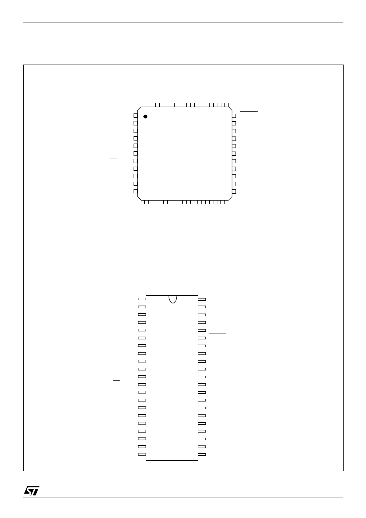
2 PIN DESCRIPTION
Figure 2. 44-pin TQFP and 42-Pin SDIP Package Pinouts
44 43 42 41 40 39 38 37 36 35 34
33
32
31
30
29
28
27
26
25
24
23
12 13 14 15 16 17 18 19 20 21 22
1
2
3
4
5
6
7
8
9
10
11
38
37
36
35
34
33
32
31
30
29
28
27
16
15
1
2
3
4
5
6
7
8
9
10
11
12
13
14
39
40
41
42
PD6
PD5
OSCOUT
OSCIN
IT9 / PC2
IT10 / SCK / PC3
IT11 / SS
/ PC4
IT12 / MISO / PC5
MOSI / PC6
PD1
V
PP
PD2
PD3
PD4
PC7
PD0
V
DDA
USBVCC
PB1 (HS) / RDI
PB0 (HS) / MC O
PA7 / AIN7
PA6 / AIN6
PA5 / AIN5
PA4 / AIN4
PA3 / AIN3 / IT4
PA0 / AIN0 / IT1 / USBOE
RESET
V
SSA
USBDM
USBDP
PA1 / AIN1 / IT2
PA2 / AIN2 / IT3
21
20
17
18
19
IT8 / PWM1 / PB7 (HS)
PC0
PC1
V
DD
V
SS
26
25
24
23
22
PB6 (HS) / PWM0 / IT7 / ICCDATA
PB5 (HS) / ARTIC2 / IT6 / ICCCLK
PB4 (HS) / ARTIC1 / IT5
PB3 (HS) / ARTCLK
PB2 (HS) / TDO
OSCOUT
OSCIN
IT9 / PC2
IT10 / SCK / PC3
IT11 / SS
/ PC4
IT12 / MISO / PC5
MOSI / PC6
PD1
V
PP
PC7
PD0
IT8 / PWM1 / PB7
PC0
PC1
V
DD
V
SS
ARTCLK / PB3 (HS)
IT5 / ARTIC1 / PB4 (HS)
ICCCLK / IT6 / ARTIC2 / PB5 (HS)
ICCDATA /IT7 / PWM0 / PB6 (HS)
N.C.
TDO / PB2 (HS)
PB1 (HS) / RDI
PB0 (HS) / MCO
PA7 / AIN7
PA6 / AIN6
PA5 / AIN5
PA4 / AIN4
PA3 / AIN3 / IT4
PA0 / AIN0 / IT1 / USBOE
RESET
PA1 / AIN1 / IT2
PA2 / AIN2 / IT3
V
DDA
USBVCC
V
SSA
USBDM
USBDP
PD3
PD4
Reserved*
PD6
PD5
PD2
* Pin 39 of the T QFP44 package
must be lef t unconnected.

ST7262
6/132
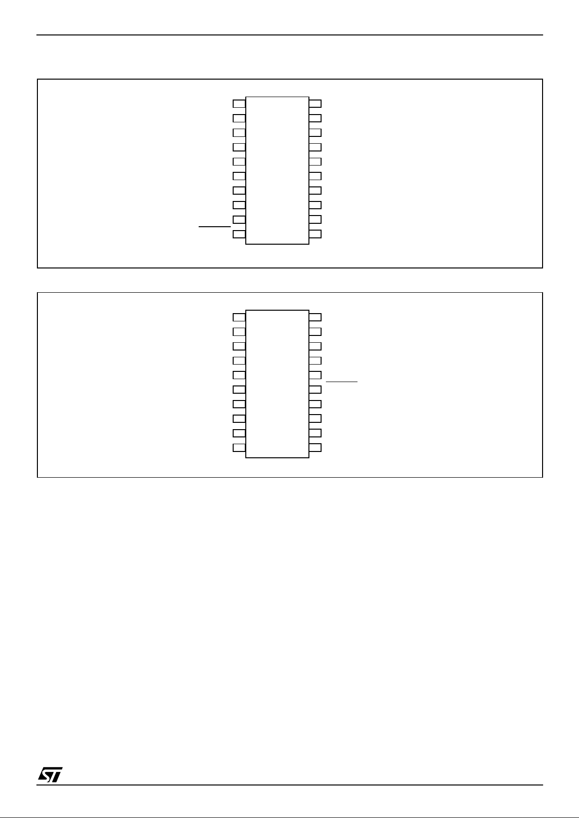
PIN DESCRIPTION (Cont’d)
Figure 3. 34-Pin SO and 32-Pin SDIP Package Pinouts
28
27
26
25
24
23
22
21
20
19
18
29
30
31
32
PC4 / SS / INT11
PC5 / MISO / IT12
PA4 / AIN4
PA3 / AIN3 / IT4
PA2 / AIN2 / IT3
PA1 / AIN1 / IT2
PA0 / AIN0 / IT1 / USBOE
V
SSA
USBDM
USBVCC
V
DDA
V
PP
RESET
PC6 / MOSI
USBDP
PC7
16
15
1
2
3
4
5
6
7
8
9
10
11
12
13
14
IT10 / SCK / PC3
IT9 / PC2
AIN7 / PA7
MCO / PB0 (HS)
RDI / PB1 (HS)
TDO / PB2 (HS)
ARTCLK / PB3 (HS)
IT5 / ARTIC1 / PB4 (HS)
ICCCLK / IT6 /ARTIC2 / PB5 (HS)
IT8 / PWM1 / PB7 (HS)
V
DD
V
SS
OSCOUT
OSCIN
ICCDATA / IT7 / PWM0 / PB6 (HS)
PA5 / AIN5
AIN6 / PA6
33
34
17
28
27
26
25
24
23
22
21
20
19
18
17
16
15
1
2
3
4
5
6
7
8
9
10
11
12
13
14
29
30
31
32
IT10 / SCK / PC3
IT9 / PC2
AIN7 / PA7
MCO / PB0 (HS)
RDI / PB1 (HS)
TDO / PB2 (HS)
ARTCLK / PB3 (HS)
IT5 / ARTIC1 / PB4 (HS)
ICCCLK / IT6 / ARTIC2 / PB5 (HS)
IT8 / PWM1 / PB7 (HS)
V
DD
V
SS
OSCOUT
OSCIN
ICCDATA / IT7 / PWM0 / PB6 (HS)
AIN6 / PA6
PC4 / SS
/ INT11
PC5 / MISO / IT12
PA4 / AIN4
PA3 / AIN3 / IT4
PA2 / AIN2 / IT3
PA1 / AIN1 / IT2
PA0 / AIN0 / IT1 / USBOE
V
SSA
USBDM
USBVCC
V
DDA
V
PP
RESET
PC6 / MOSI
USBDP
PA5 / AIN5
PC1
ST7262
7/132
Figure 4. 20-pin SO20 Package Pinout
Figure 5. 20-pin DIP20 Package Pinout
14
13
12
11
15
16
17
18
OSCIN
OSCOUT
PB7 (HS) / PWM1 / IT8
PB6 (HS) / PWM0 / IT7/ ICCDATA
USBVCC
V
DD
V
PP
USBDP
1
2
3
4
5
6
7
8
9
10
IT3 / AIN2 / PA2
PB0 (HS) / MCO
PB1 (HS)
PB2 (HS)
PB3 (HS) / ARTCLK
PB4 (HS) / ARTIC1 / IT5
RESET
IT2 / AIN1 / PA1
19
20
USBOE/ IT1 / AIN0/ PA0
V
SS
USBDM
PB5 (HS) / ARTIC2 / IT6 / ICCCLK
14
13
12
11
15
16
17
18
OSCIN
OSCOUT
PB7 (HS) / PWM1 / IT8
PB6 (HS) / PWM0 / IT7/ICCDATA
USBVCC
V
DD
V
PP
USBDP
1
2
3
4
5
6
7
8
9
10
IT5 / ARTIC1 / PB4 (HS)
MCO / PB0 (HS)
PB1 (HS)
PB2 (HS)
RESET
IT2 / AIN1/ PA1
19
20
USBOE / IT1 / AIN0 / PA0
V
SS
USBDM
PB5 (HS) / ARTIC2 / IT6 / ICCCLK
IT3 / AIN2 / PA2
ARTCLK / PB3 (HS)
ST7262
8/132
PIN DESCRIPTION (Cont’d)
Legend / Abbreviations:
Type: I = Input, O = Output, S = Supply
Input level: A = Dedicated analog input
Input level: C = CMOS 0.3V
DD
/0.7VDD,
C
T
= CMOS 0.3VDD/0.7VDD with input trigger
Output level: HS = High Sink (on N-buffer only)
Port configuration capabilities:
– Input:float = floatin g, wpu = weak pull-up, int = interrupt (\ =falling edge, / =rising edge
),
ana = analog
– Output: OD = open drain, T = true open drain (N buffer 8mA@0.4 V), PP = push-pull
Table 1. Device Pin Description
Pin n°
Pin Name
Type
Level Port / Control
Main
Function
(after
reset)
Alternate Function
TQFP44
DIP42
SO34
DIP32
SO20
DIP20
Input
Output
Input Output
float
wpu
int
ana
OD
PP
1 6 29 28 9 14 V
PP
Sx
FLASH programming voltage
(12V), must be tied low in user
mode.
2 7 - - - - PD1 I/O C
T
xxPort D1
3 8 - - - - PD0 I/O C
T
xxPort D0
4 9 31 - - - PC7 I/O C
T
xxPort C7
5 10 32 30 - - PC6/MOSI I/O C
T
xxPort C6
SPI Master Out /
Slave In
1)
6 11 33 31 - - PC5/MISO/IT12 I/O C
T
xx xPort C5
SPI Master In /
Slave Out 1) /
Interrupt 12 input
7 12 34 32 - - PC4/SS
/IT11 I/O C
T
xx xPort C4
SPI Slave Select
(active low) 1)/
Interrupt 11 input
8 13 1 1 - - PC 3/SCK /IT10 I/O C
T
xx xPort C3
SPI Serial Clock
1)
/
Interrupt 10 input
9 14 2 2 - - PC2/IT9 I/O C
T
xx xPort C2 Interrupt 9 input
10 15 3 3 11 16 OSCIN
These pins are used connect an
external clock source to the onchip main oscillator.
11 16 4 4 12 17 OSCOUT
12175549V
SS
S Digital Ground Voltage
13 18 6 6 8 13 V
DD
S
Digital Main Power Supply Voltage
14 19 7 - - - PC1 I/O C
T
xTPort C1
15 20 - - - - PC0 I/O C
T
xTPort C0
16 21 8 7 13 18
PB7/PWM1/IT8/
RX_SEZ/DATAOUT/DA9
I/O C
T
HS x \ x Port B7
ART PWM output 1/
Interrupt 8 input
17 - - N.C. Not Connected

ST7262
9/132
18 22 9 8 14 19
PB6/PWM0/IT7/
ICCDATA
I/O CTHS x \ x Port B6
ART PWM output 0/
Interrupt 7 input/InCircuit Communication Data
19 23 10 9 15 20
PB5/ARTIC2/IT6/
ICCCLK
I/O C
T
HS x / x Port B5
ART Input Capture 2/
Interrupt 6 input/
In-Circuit Communication Clock
20 24 11 10 16 1 PB4/ARTIC1/IT5 I/O C
T
HS x / x Port B4
ART Input Capture
1/Interrupt 5 input
21 25 12 11 17 2 PB3/ARTCLK I/O C
T
HS x x Port B3 ART Clock input
22 26 13 12 18 3 PB2/TDO I/O C
T
HS x x Port B2
SCI Transmit Data
Output
1)
23 27 14 13 19 4 PB1/RDI I/O CTHS x x Port B1
SCI Receive Data
Input
1)
24 28 15 14 20 5 PB0/MCO I/O CTHS x x Port B0 CPU clock output
25 29 16 15 - - PA7/AIN7 I/O C
T
xxxPort A7 ADC Analog Input 7
26 30 17 16 - - PA6/AIN6 I/O C
T
xxxPort A6 ADC Analog Input 6
27 31 18 17 - - PA5/AIN5 I/O C
T
xxxPort A5 ADC Analog Input 5
28 32 19 18 - - PA4/AIN4 I/O C
T
xxxPort A4 ADC Analog Input 4
29 33 20 19 - - PA3/AIN3/IT4 I/O C
T
x\xxPort A3
ADC Analog Input 3/
Interrupt 4 input
30 34 21 20 1 6 PA2/AIN 2/IT3 I/O C
T
x\xxPort A2
ADC Analog Input 2/
Interrupt 3 input
31 35 22 21 2 7 PA1/AIN 1/IT2 I/O C
T
x\xxPort A1
ADC Analog Input 1/
Interrupt 2 input
32 36 23 22 3 8
PA0/AIN0/IT1 /
USBOE
I/O C
T
x\xxPort A0
ADC Analog Input 0/
Interrupt 1 input/
USB Output Enable
33 37 30 29 10 15 RESET
I/O C
Top priority non maskable interrupt (active low)
34 38 24 23 - - V
SSA
S
Analog Ground Voltage, must
be connected externally to V
SS
.
35 39 25 24 5 10 USBDM I/O USB bidirectional data (data -)
36 40 26 25 6 11 USBDP I/O USB bidirectional data (data +)
37 41 27 26 7 12 USBVCC S USB power supply 3.3V output
38 42 28 27 - - V
DDA
S
Analog Power Supply Voltage,
must be connected externally to
V
DD
.
39 - - - - - Reserved Must be left unconnected.
40 1 - - - - PD6 I/O C
T
xxPort D6
41 2 - - - - PD5 I/O C
T
xxPort D5
42 3 - - - - PD4 I/O C
T
xxPort D4
Pin n°
Pin Name
Type
Level Port / Control
Main
Function
(after
reset)
Alternate Function
TQFP44
DIP42
SO34
DIP32
SO20
DIP20
Input
Output
Input Output
float
wpu
int
ana
OD
PP
ST7262
10/132
Note 1: Peripheral not present on all devices. Refer to “Device Summary” on page 1.
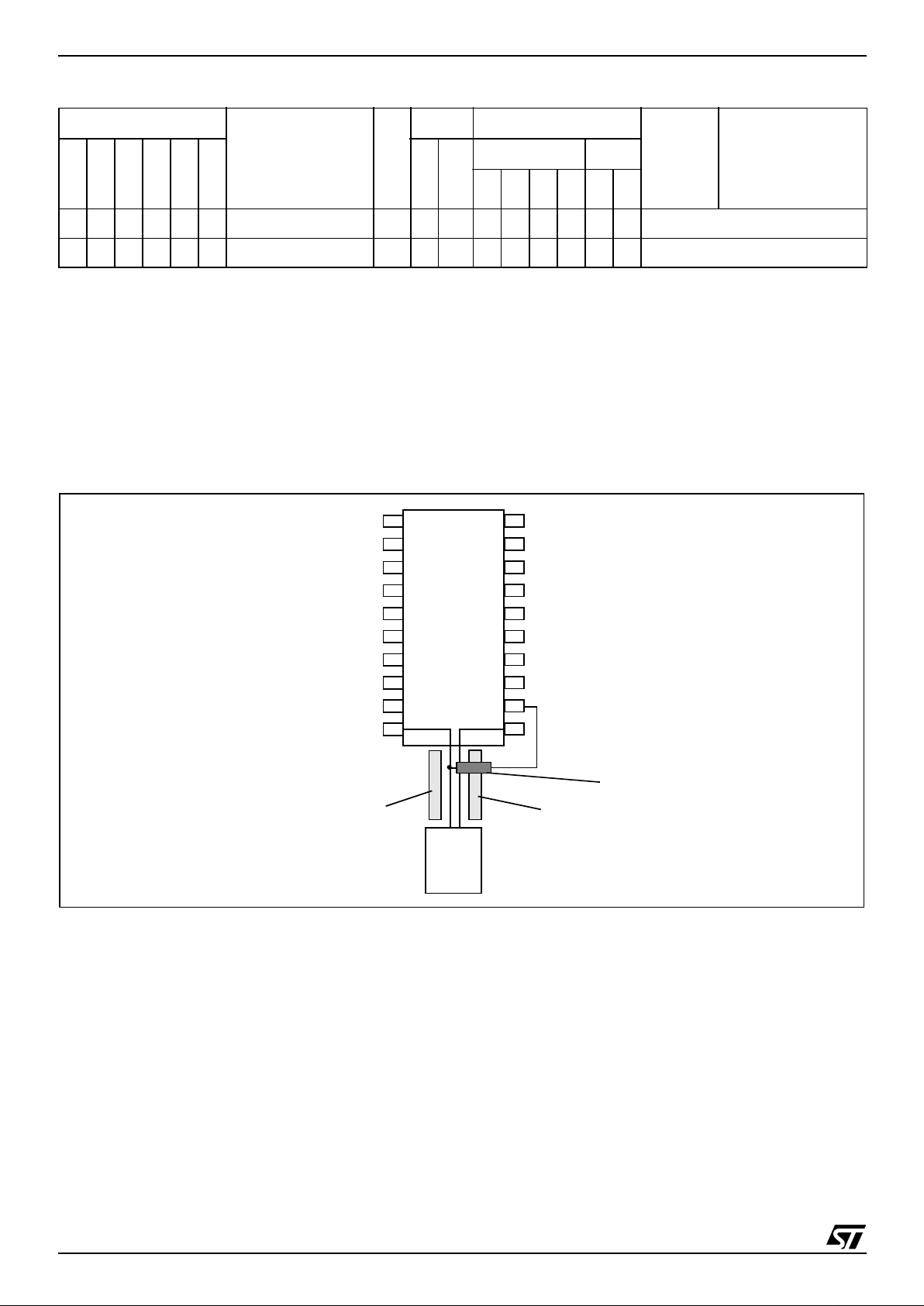
2.1 PCB LAYOUT RECOMMENDATION
In the case of DIP20 de vices the user s hould layout the PCB so that the DIP20 ST7262 device and
the USB connector are centered on the same axis
ensuring that the D- and D+ lines are of equal
length. Refer to Figure 6
Figure 6. Recommended PCB Layout for USB Interface with DIP20 package
43 4 - - - - PD3 I/O C
T
xxPort D3
44 5 - - - - PD2 I/O C
T
xxPort D2
Pin n°
Pin Name
Type
Level Port / Control
Main
Function
(after
reset)
Alternate Function
TQFP44
DIP42
SO34
DIP32
SO20
DIP20
Input
Output
Input Output
float
wpu
int
ana
OD
PP
14
13
12
11
15
16
17
18
USBVCC
USBDP
1
2
3
4
5
6
7
8
9
10
19
20
USBDM
USB Connect o r
Ground
Ground
ST7262
1.5KOhm pull-up resistor
ST7262
11/132
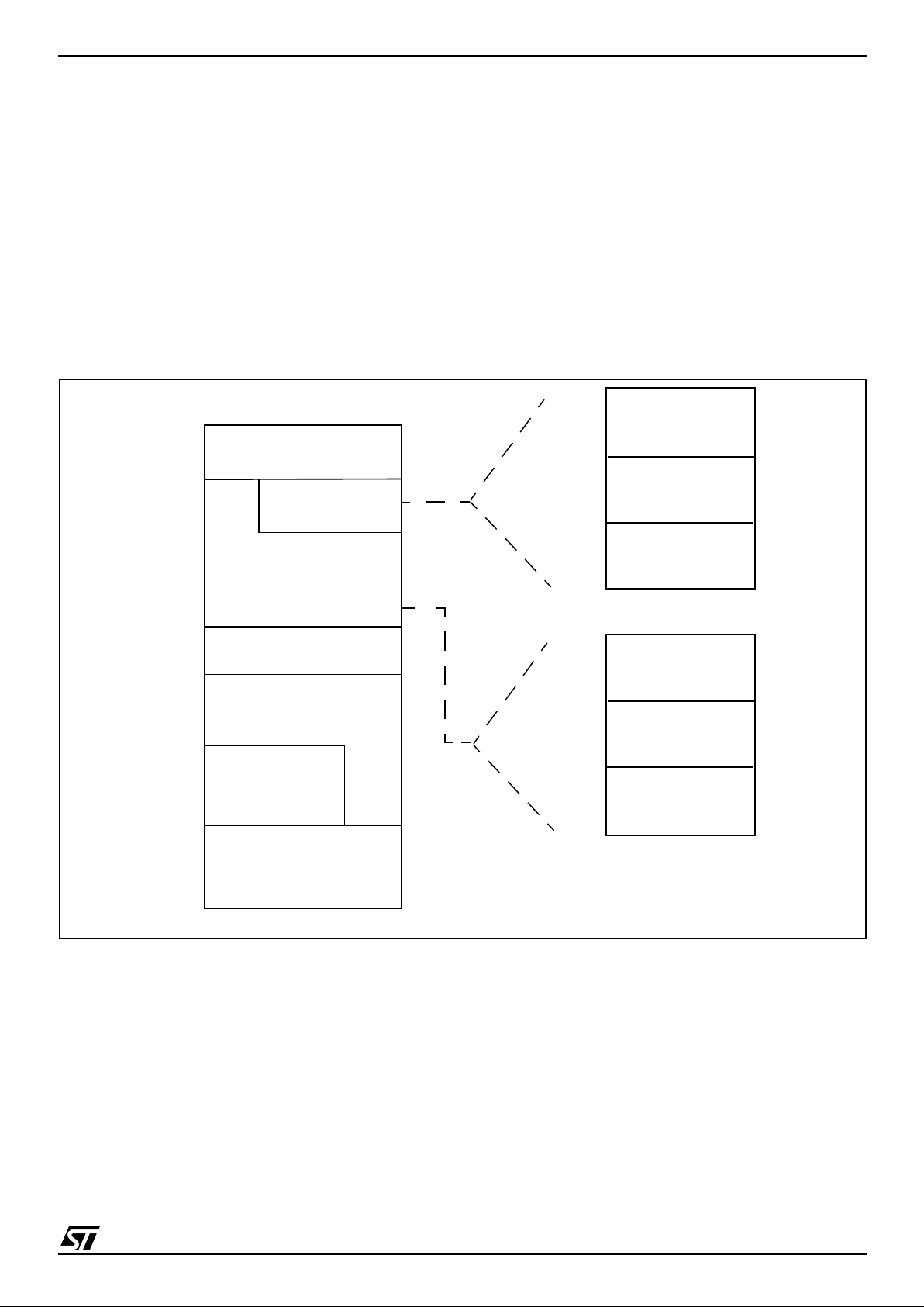
3 REGISTER & MEMORY MAP
As shown in the Figure 7, the MCU i s capable of
addressing 64K bytes of memories and I/O registers.
The available memory locations consist of 64
bytes of register locations, 768 bytes of RA M and
up to 16 Kbytes of user program memory. The
RAM space includes u p to 128 by t es fo r the stack
from 0100h to 017Fh.
The highest address b ytes contain the user res et
and interrupt vectors.
IMPORTANT: Memory locations marked as “Reserved” must ne ver be accessed. A ccessi ng a reseved area can have u npredict able effects on the
device.
Figure 7. Me m ory M a p
0000h
Program Memory
Interrupt & Reset Vectors
HW Registers
BFFFh
0040h
003Fh
(see Table 2)
C000h
FFDFh
FFE0h
FFFFh
(see Table 6)
0340h
Reserved
033Fh
Short Addressing
RAM (zero page)
or Stack
017Fh
0040h
00FFh
768 Bytes RAM
E000h
8 KBytes
(128 Bytes)
16 KBytes
384 Bytes RAM
64 Bytes
01BFh
16-bit Addressing
RAM
Short Addressing
RAM (zero page)
017Fh
0040h
00FFh
448 Bytes
033Fh
16-bit Addressing
RAM
16-bit Addressing
RAM
or Stack
(128 Bytes)
16-bit Addressing
RAM
192 Bytes
192 Bytes

ST7262
12/132
Table 2. Hardware Register M ap
Address Block
Register
Label
Register Name
Reset
Status
Remarks
0000h
0001h
Port A
PADR
PADDR
Port A Data Register
Port A Data Direction Register
00h
1)
00h
R/W
2)
R/W
2)
0002h
0003h
Port B
PBDR
PBDDR
Port B Data Register
Port B Data Direction Register
00h
1)
00h
R/W
2)
R/W
2)
0004h
0005h
Port C
PCDR
PCDDR
Port C Data Register
Port C Data Direction Register
00h
1)
00h
R/W
2)
R/W
2)
0006h
0007h
Port D
PDDR
PDDDR
Port D Data Register
Port D Data Direction Register
00h
1)
00h
R/W
2)
R/W
2)
0008h ITRFRE1 Interrupt Register 1 00h R/W
0009h MISC Miscellaneous Register 00h R/W
000Ah
000Bh
000Ch
ADC
ADCDRMSB
ADCDRLSB
ADCCSR
ADC Data Register (bit 9:2)
ADC Data Register (bit 1:0)
ADC Control Status Register
00h
00h
00h
Read Only
Read Only
R/W
000Dh WDG WDGCR Watchdog Control Register 7Fh R/W
000Eh
0010h
Reserved Area (3 Bytes)
0011h
0012h
0013h
SPI
SPIDR
SPICR
SPICSR
SPI Data I/O Register
SPI Control Register
SPI Control Status Register
xxh
0xh
00h
R/W
R/W
Read Only
0014h
0015h
0016h
0017h
0018h
0019h
001Ah
001Bh
001Ch
PWM ART
PWMDCR1
PWMDCR0
PWMCR
ARTCSR
ARTCAR
ARTARR
ARTICCSR
ARTICR1
ARTICR2
PWM AR Timer Duty Cycle Register 1
PWM AR Timer Duty Cycle Register 0
PWM AR Timer Control Register
Auto-Reload Timer Control/Status Register
Auto-Reload Timer Counter Access Register
Auto-Reload Timer Auto-Reload Register
ART Input Capture Control/Status Register
ART Input Capture Register 1
ART Input Capture Register 2
00h
00h
00h
00h
00h
00h
00h
00h
00h
R/W
R/W
R/W
R/W
R/W
R/W
R/W
Read Only
Read Only
001Dh
001Eh
001Fh
0020h
0021h
0022h
0023h
0024h
SCI
SCIERPR
SCIETPR
SCISR
SCIDR
SCIBRR
SCICR1
SCICR2
SCI Extended Receive Prescaler register
SCI Extended Transmit Prescaler Register
Reserved Area
SCI Status register
SCI Data register
SCI Baud Rate Register
SCI Control Register 1
SCI Control Register 2
00h
00h
--
C0h
xxh
00h
x000 0000b
00h
R/W
R/W
Read Only
R/W
R/W
R/W
R/W

ST7262
13/132
Legend: x=undefined, R/W=read/write
Notes:
1. The contents of the I/O port DR regist ers are readable only in out put conf iguration. I n i nput conf iguration, the values of the I/O pins are returned instead of the DR register contents.
2. The bits associated with unavailable pins must always be kept at their reset value.
0025h
0026h
0027h
0028h
0029h
002Ah
002Bh
002Ch
002Dh
002Eh
002Fh
0030h
0031h
USB
USBPIDR
USBDMAR
USBIDR
USBISTR
USBIMR
USBCTLR
USBDADDR
USBEP0RA
USBEP0RB
USBEP1RA
USBEP1RB
USBEP2RA
USBEP2RB
USB PID Register
USB DMA Address register
USB Interrupt/DMA Register
USB Interrupt Status Register
USB Interrupt Mask Register
USB Control Register
USB Device Address Register
USB Endpoint 0 Register A
USB Endpoint 0 Register B
USB Endpoint 1 Register A
USB Endpoint 1 Register B
USB Endpoint 2 Register A
USB Endpoint 2 Register B
x0h
xxh
x0h
00h
00h
06h
00h
0000 xxxxb
80h
0000 xxxxb
0000 xxxxb
0000 xxxxb
0000 xxxxb
Read Only
R/W
R/W
R/W
R/W
R/W
R/W
R/W
R/W
R/W
R/W
R/W
R/W
0032h
to
0035h
Reserved Area (4 Bytes)
0032h
0033h
0034h
0035h
ITC
ITSPR0
ITSPR1
ITSPR2
ITSPR3
Interrupt Software Priority Register 0
Interrupt Software Priority Register1
Interrupt Software Priority Register 2
Interrupt Software Priority Register 3
FFh
FFh
FFh
FFh
R/W
R/W
R/W
R/W
0036h
0037h
TBU
TBUCV
TBUCSR
TBU Counter Value Register
TBU Control/Status Register
00h
00h
R/W
R/W
0038h FLASH FCSR Flash Control/Status Register 00h R/W
0039h ITRFRE2 Interrupt Register 2 00h R/W
003Ah
to
003Fh
Reserved Area (6 Bytes)
Address Block
Register
Label
Register Name
Reset
Status
Remarks

ST7262
14/132
4 FLASH PROGRAM MEMORY
4.1 Introduction
The ST7 dual voltage High Density Flash
(HDFlash) is a non-volatile memory that can be
electrically erased as a single block or by individual sectors and programmed on a Byte-by-Byte basis using an external V
PP
supply.
The HDFlash devices can be programmed and
erased off-board (plugge d in a programm ing tool)
or on-board using ICP (In-Circuit Programming) or
IAP (In-Application Programming).
The array matrix organ isation allows each sector
to be erased and reprogramm ed without affecting
other sectors.
4.2 Main Features
■ Three Flash programming modes :
– Insertion in a programming tool. In this m ode,
all sectors including option bytes can be programmed or erased.
– ICP (In-Circuit Programming). In this mode, all
sectors including option bytes can be programmed or erased without removing the device from the application board.
– IAP (In-Application Programming) In this
mode, all sectors except Sector 0, can be programmed or erased without removing the device from the application board a nd wh ile the
application is running.
■ ICT (In-Circuit Testing) for downloading and
executing user application test patterns in RAM
■ Read-out protection against piracy
■ Register Access Security System (RASS) to
prevent accidental programming or erasing
4. 3 S truct u re
The Flash memory is organised in sectors and can
be used for both code and data storage.
Depending on the overall Flash memory size in the
microcontroller device, there are up to three user
sectors (see Tab le 3). Each of these sectors can
be erased independently to avoid unnecessary
erasing of the whole Flas h memory when only a
partial erasing is required.
The first two sectors have a fixed siz e of 4 Kby tes
(see Figure 8). They are mapped in the upper part
of the ST7 addressing space so t he reset and interrupt vectors are located in Sector 0 (F000hFFFFh).
Table 3. Sectors available in Flash devices
4.3.1 Read-out Protection
Read-out protection, when s elected, makes it impossible to extract the memory content from the
microcontroller, thus preventing piracy. Even ST
cannot access the user code.
In flash devices, this protection is removed by reprogramming the option. In this case, the entire
program memory is first automatically erased and
the device can be reprogrammed.
Read-out protection selection depend s on the device type:
– In Flash devices it is enabled and removed
through the FMP_R bit in the option byte.
– In ROM devices it is enabled by mask option
specified in the Option List.
Figure 8. Me m ory M a p and Sector A dd r ess
Flash Size (bytes) Available Sectors
4K Sector 0
8K Sectors 0,1
> 8K Sectors 0,1, 2
4 Kbytes
4 Kbytes
2Kbytes
SECTOR 1
SECTOR 0
16 Kbytes
SECTOR 2
8K 16K 32K 60K
FLASH
FFFFh
EFFFh
DFFFh
3FFFh
7FFFh
1000h
24 Kbytes
MEMORY SIZE
8Kbytes 40 Kbytes
52 Kbytes
9FFFh
BFFFh
D7FFh
4K 10K 24K 48K

ST7262
15/132
FLASH PROGRAM MEMORY (Cont’d)
4.4 ICC Interface
ICC needs a m inimum of 4 and up to 6 pins to b e
connected to the programming tool (see Figure 9).
These pins are:
– RESET
: device reset
–V
SS
: device power supply ground
– ICCCLK: ICC output serial clock pin
– ICCDATA: ICC input/output serial data pin
– ICCSEL/V
PP
: programming voltage
– OSC1(or OSCIN): main clock in put for exter-
nal source (optional)
–V
DD
: application board power su pply (option-
al, see Figure 9, Note 3)
Figure 9. Typical ICC Interface
Notes:
1. If the ICCCLK or ICCDATA pins are only u sed
as outputs in t he ap plication, n o s ign al iso lation is
necessary. As soon as the Programming Tool is
plugged to the board, even if an ICC session is not
in progress, the ICCCLK and ICCDATA pins are
not available for the application. If they are used as
inputs by the application, isolation such as a serial
resistor has to implemented in case another device forces the signal. Refer to the Programming
Tool documentation for recommended resistor values.
2. During the ICC session, the programming tool
must control the RESET
pin. This can lead to conflicts between the programming tool and the application reset circuit if it drives more than 5mA at
high level (push pull output or pull-up resistor<1K).
A schottky diode can be us ed to iso late the application RESET circuit in this case. When using a
classical RC network with R>1K or a reset man-
agement IC with open drain ou tput and pu ll-up resistor>1K, no additional com ponents are needed.
In all cases the user must ensure that no external
reset is generated by the application during the
ICC session.
3. The use of Pin 7 of the ICC con nector de pends
on the Programming Tool architecture. This pin
must be connected when using most ST Programming Tools (it is used to monitor the application
power supply). Please refer to the Programming
Tool manual.
4. Pin 9 has to be co nnected to the OS C1 or OSCIN pin of the ST7 when the clock is not available
in the application or if the sel ected clock opt ion is
not programmed in t he option byte. ST7 devices
with multi-oscillator capability need to have OSC2
grounded in this case.
ICC CONNECTOR
ICCDATA
ICCCLK
RESET
V
DD
HE10 CONNECTOR TYPE
APPLICATION
POWER SUPPLY
1
246810
975 3
PROGRAMMING TOOL
ICC CONNECTOR
APPLICATION BOARD
ICC Cab le
OPTIONAL
(See No te 3)
10k
Ω
V
SS
ICCSEL/VPP
ST7
C
L2
C
L1
OSC1
OSC2
OPTIONAL
See Note 1
See Note 2
APPLICATION
RESET SOURCE
APPLICATI ON
I/O
(See No te 4)

ST7262
16/132
FLASH PROGRAM MEMORY (Cont’d)
4.5 ICP (In-Circuit Programming)
To perform ICP the microcontroller must be
switched to ICC (In-Circuit Communication) mode
by an external controller or programming tool.
Depending on the ICP code dow nloaded in RAM,
Flash memory programming can be fully customized (number of bytes to prog ram, program locations, or selection serial communication interface
for downloading).
When using an STMicroelectronics or third-party
programming tool that supp orts ICP and the specific microcontroller device, the user needs only to
implement the ICP hardware interface on the application board (see Figure 9). For more details on
the pin locations, refer to the device pinout description.
4.6 IA P ( I n-Application Programming)
This mode uses a BootLoader program previously
stored in Sector 0 by the us er (in ICP mode or by
plugging the device in a programming tool).
This mode is fully controlled by user software. This
allows it to be adapted to the user application, (user-defined strategy for entering programming
mode, choice of comm unications protocol used to
fetch the data to be stored, etc.). For example, it is
possible to download code from the SPI, SCI, USB
or CAN interface and program it in the Fl ash. IAP
mode can be used to program any of the Flash
sectors except Sector 0, which i s write/erase protected to allow recovery in case errors occur during the programming operation.
4.7 Related Documentation
For details on Flash program ming and ICC protocol, refer to the ST7 Flash Programming Reference Manual and to the ST7 ICC Protocol Re ference Manual
.
4.8 Register Description
FLASH CONTROL/STATUS REGISTER (FCSR)
Read/Write
Reset Value: 0000 0000 (00h)
This register is reserved for use by Programming
Tool software. It controls the Flash programming
and erasing operations.
70
00000000
ST7262
17/132
5 CENTRAL PRO CESSING UNIT
5.1 INTRODUCTION
This CPU has a full 8-bit architecture and contains
six internal registers allowing efficient 8-bit data
manipulation.
5.2 MAIN FEATURES
■ Enable executing 63 basic instructions
■ Fast 8-bit by 8-bit multiply
■ 17 main addressing modes (with indirect
addressing mode)
■ Two 8-bit index registers
■ 16-bit stack pointer
■ Low power HALT and WAIT modes
■ Priority maskable hardware interrupts
■ Non-maskable software/hardware interrupts
5.3 CPU REGISTERS
The 6 CPU registers shown in Figure 10 are not
present in the memory mapping and are accessed
by spec ifi c ins t ru c tio n s .
Accumulator (A)
The Accumulator is an 8-bit general purpose register used to hold operands and the res ults of the
arithmetic and logic calculations and to manipulate
data.
Index Registers (X and Y)
These 8-bit registers are used to create effective
addresses or as tempo rary storage areas f or data
manipulation. (The Cross -Assembler generates a
precede instruction (PRE) to indicate that the following instruction refers to the Y register.)
The Y register is not affected by the interrupt automatic procedures.
Program Counter (PC)
The program counter is a 16-bit register containing
the address of the next instruction to be executed
by the CPU. It is made of two 8-bit registers PCL
(Program Counter Low which is the LSB) and PCH
(Program Counter High which is the MSB).
Figure 10. CPU Registers
ACCUMULATOR
X INDEX REGISTER
Y INDEX REGISTER
STACK POINTER
CONDITION CODE REGISTER
PROGRAM COUNTER
70
1C1I1HI0NZ
RESET VALUE = RESET VECTOR @ FFFEh-FFFFh
70
70
70
0
7
15 8
PCH
PCL
15
8
70
RESET VALUE = STACK HIGHER ADDRESS
RESET VALUE =
1X11X1XX
RESET VALUE = XXh
RESET VALUE = XXh
RESET VALUE = XXh
X = Undefined Value

ST7262
18/132
CENTRAL PROC ESSING UNIT (Cont’d)
Condition Code Reg ister (CC)
Read/Write
Reset Value: 111x1xxx
The 8-bit Condition Code regist er contains the i nterrupt masks and four flags representative of the
result of the instruction just executed. This register
can also be handled by the PUSH and POP instructions.
These bits can be individually tested and/or controlled by specific instructions.
Arithmetic Management Bits
Bit 4 = H
Half carry
.
This bit is set by hardware when a carry occurs between bits 3 and 4 of t he ALU during an ADD or
ADC instructions. It is reset by hardware during
the same instructio n s.
0: No half carry has occurred.
1: A half carry has occurred.
This bit is tested using the JRH or JRNH in struction. The H bit is useful in BCD arithmetic subroutine s .
Bit 2 = N
Negative
.
This bit is set and cleared by hardware. It is representative of the result sign of the last arithmetic,
logical or data manipulation. I t’s a copy of the result 7
th
bit.
0: The result of the last operation is positive or null.
1: The result of the last operation is negative
(i.e. the most significant bit is a logic 1).
This bit is accesse d by the JRMI and JRPL instructions.
Bit 1 = Z
Zero
.
This bit is set and cleared by hardware. This bit indicates that the result of the last arithme tic, logical
or data manipulation is zero.
0: The result of the last operation is dif ferent from
zero.
1: The result of the last operation is zero.
This bit is accessed by the JREQ and JRNE test
instructions.
Bit 0 = C
Carry/borrow.
This bit is set and cleared b y hardware and software. It indicates an overflow or an un derflow has
occurred during the last arithmetic operation.
0: No overflow or underflow has occurred.
1: An overflow or underflow has occurred.
This bit is driven by th e SCF and RCF instructions
and tested by the JRC and JRNC instructions. It i s
also affected by the “bit test and branch”, shift and
rotate instructions.
Interrupt Managem e nt B i ts
Bit 5,3 = I1, I0
Interrupt
The combination of the I1 and I0 bits gives the current interrupt software priority.
These two bits are set/cleared by hardware when
entering in interrupt. The loaded value is given by
the corresponding bits in the interrupt software priority registers (IxSPR). They can be also set/
cleared by software with the RIM, SIM, IRET,
HALT, WFI and PUSH/POP instructions.
See the interrupt management chapter for more
details.
70
11I1HI0NZ
C
Interrupt Software Priorit y I1 I0
Level 0 (main) 1 0
Level 1 0 1
Level 2 0 0
Level 3 (= interrupt disable) 1 1

ST7262
19/132
CPU REGISTERS (Cont’d)
STACK POINTER (SP)
Read/Write
Reset Value: 017Fh
The Stack Pointer is a 16-bit register which is always pointing to the next free location in the stack.
It is then decremented after data has been pushed
onto the stack and incremented before data is
popped from the stack (see Figure 11).
Since the stack is 128 bytes deep, the 9 most significant bits are forced by hard ware. Following a n
MCU Reset, or after a Reset Stack Pointer instruction (RSP), the Stack Pointer contains its reset value (the SP6 to SP0 bits are set) which is the stack
higher address.
The least significant byte of the Stack Pointer
(called S) can be directly accessed by a LD instruction.
Note: When the lower limit is exceeded, the Stack
Pointer wraps around to the stack upper limit, without indicating the stack overflow. The previously
stored information is then o verwritten and therefore lost. The stack also wraps in case of an underflow.
The stack is used to sav e the return address during a subroutine call and the CPU context during
an interrupt. The user may also directly manipulate
the stack by means of the PUSH and POP instructions. In the case of an interrupt, the PCL is stored
at the first location po inted t o by t he SP. Th en t he
other registers are stored in the next locations as
shown in Figure 11.
– When an interrupt is received, the SP is decre-
mented and the context is pushed on the stack.
– On return from interrupt, the SP is incremented
and the context is popped from the stack.
A subroutine call occupies two locations and an interrupt five locat ion s i n the stack ar ea.
Figure 11. Stack Manipulation Examp le
15 8
00000001
70
1 SP6 SP5 SP4 S P3 SP2 S P1 SP0
PCH
PCL
SP
PCH
PCL
SP
PCL
PCH
X
A
CC
PCH
PCL
SP
PCL
PCH
X
A
CC
PCH
PCL
SP
PCL
PCH
X
A
CC
PCH
PCL
SP
SP
Y
CALL
Subroutine
Interrupt
Event
PUSH Y POP Y IRET
RET
or RSP
@ 017Fh
@ 0100h
Stack Higher Address = 017Fh
Stack Lower Address =
0100h
ST7262
20/132
6 CLOCKS AND RESET
6.1 CLOCK SYSTEM
6.1.1 General Description
The MCU accepts either a Crystal or Ceramic resonator, or an external clock signal to drive the internal oscillator. The internal clock (f
CPU
) is de-
rived from the external oscillator frequency (f
OSC
),
by dividing by 3 and multiplying by 2. By setting the
OSC12/6 bit in the option byte, a 12 MHz ex ternal
clock can be used giving an internal frequency of 8
MHz while maintaining a 6 MHz clock for USB (refer to Figure 14).
The internal clock signal (f
CPU
) consists of a
square wave with a duty cycle of 50%.
It is further divided by 1, 2, 4 or 8 depending on the
Slow Mode Selection bits in the Miscellaneous
register ( SMS[1:0 ])
The internal oscillat or is designed to operate with
an AT-cut parallel resonant quartz or ceramic resonator in the frequency range specified for f
osc
.
The circuit shown in Figure 13 is recommended
when using a crystal, and Table 4 lists the recommended capacitors. The crystal and associated
components shoul d be m ounted as close as possible to the input pins in o rder to minimize output
distortion and start-up stabilization time.
Table 4. Recommended Values for 12 MHz
Crystal Resonator
Note: R
SMAX
is the equivalent serial resistor of the
crystal (see crystal specification).
6.1.2 External Clock input
An external clock may be applied to the OSCIN input with the OSCOUT pin not connected, as
shown on Figure 12. The t
OXOV
specifications
does not apply when using an external clock input.
The equivalent specification of the external clock
source should be used instead of t
OXOV
(see Elec-
tr ical Characte ristics).
6.1.3 Clock Output Pin (MCO)
The internal clock (f
CPU
) can be output on Port B0
by setting the MCO bit in the Misce llaneous register.
Figure 12. External Clock Source Connections
Figure 13. Crystal/Ceramic Resonator
Figure 14. Clock block diagram
R
SMAX
20
Ω
25
Ω
70
Ω
C
OSCIN
56pF 47pF 22pF
C
OSCOUT
56pF 47pF 22pF
R
P
1-10 M
Ω
1-10 M
Ω
1-10 M
Ω
OSCIN OSCOUT
EXTERNAL
CLOCK
NC
OSCIN
OSCOUT
C
OSCIN
C
OSCOUT
to CPU and
f
CPU
8/4/2/1 MHz
6 MHz (USB)
12 or
peripherals
%2
0
1
OSC12/6
6 MHz
Crystal
x2
Slow
Mode
%
SMS[1:0]
1/2/4/8
%3
(or 4/2/1/0.5 MHz)
MCO pin

ST7262
21/132
6.2 RESET
The Reset procedure is used to provide an orderly
software start-up or to exit low power modes.
Three reset modes are provided: a low voltage reset, a watchdog reset and an ext ernal reset at the
RESET
pin.
A reset causes the reset vector to be fetched from
addresses FFFEh and FFFFh in order to be loaded
into the PC and with program execution starting
from this point.
An internal circuitry provides a 5 14 CPU clock cycle delay from the time that the oscillator becomes
active.
6.2.1 Low Voltage Reset
Low voltage reset circuitry generates a reset when
V
DD
is:
■ below V
IT+
when VDD is rising,
■ below V
IT-
when VDD is falling.
During low voltage reset, the RESET
pin is held low,
thus permitting the MCU to reset other devices.
The Low Voltage Detector can be disabled by setting the LVD bit of the Option byte.
6.2.2 Watchdog Reset
When a watchdo g reset occ urs, t he RESET
pin is
pulled low permitting the MCU to reset other devices as when low voltage reset (Figure 15 ).
6.2.3 External Reset
The external reset is an active low input signal applied to the RESET
pin of the MCU.
As shown in Figure 18, the RESET
signal must
stay low for a minimum of one and a half CPU
clock cycles.
An internal Schmitt trigger at the RESET
pin is pro-
vided to improve noise immunity.
Figure 15. Low Voltage Reset functional Diagram
Figure 16. Low Voltage Reset Signal Output
Note: Typical hysteresis (V
IT+-VIT-
) of 250 mV is
expected
Figure 17. Temporization Timing Diagram after an internal Reset
LOW VOLTAGE
V
DD
FROM
WATCHDOG
RESET
RESET
INTERNAL
RESET
RESET
RESET
V
DD
V
IT+
V
IT-
V
DD
Addresses
$FFFE
Temporization
V
IT+
(514 CPU clock cycles)
ST7262
22/132
Figure 18. Reset Timing Diagra m
Note: Refer to Electrical Characteristics for values of t
DDR
, t
OXOV
, V
IT+
and V
IT-.
Figure 19. Reset Block Diagram
Note: The output of the external reset circuit must have an open-drain output to drive the ST7 reset pad.
Otherwise the device can be damaged when the ST7 generates an internal reset (LVD or watchdog).
V
DD
OSCIN
f
CPU
FFFF
FFFE
PC
RESET
t
DDR
t
OXOV
514 CPU
CLOCK
CYCLES
DELAY
RESET
R
ON
V
DD
WATCHDOG RESET
LVD RESET
INTERNAL
RESET
PULSE
GENERATOR
200ns
Filter
t
w(RSTL)out
+ 128 f
OSC
delay

ST7262
23/132
7 INTERRUP T S
7.1 INTRODUCTION
The CPU enhanced interrupt management provides the following features:
■ Hardware interrupts
■ Software interrupt (TRAP)
■ Nested or concurrent interrupt management
with flexible interrupt priority and level
management:
– Up to 4 software programmable nesting levels
– Up to 16 interrupt vectors fixed by hardware
– 3 non maskable events: RESET, TRAP, TLI
This interrupt management is based on:
– Bit 5 and bit 3 of the CPU CC register (I1:0),
– Interrupt software priority registers (ISPRx),
– F ixed interrupt vecto r addresses locat ed at the
high addresses of the memory map (FFE0h to
FFFFh) sorted by hardware priority order.
This enhanced interrupt cont roller guarantees full
upward compatibility with the standard (not nested) CPU interrupt controller.
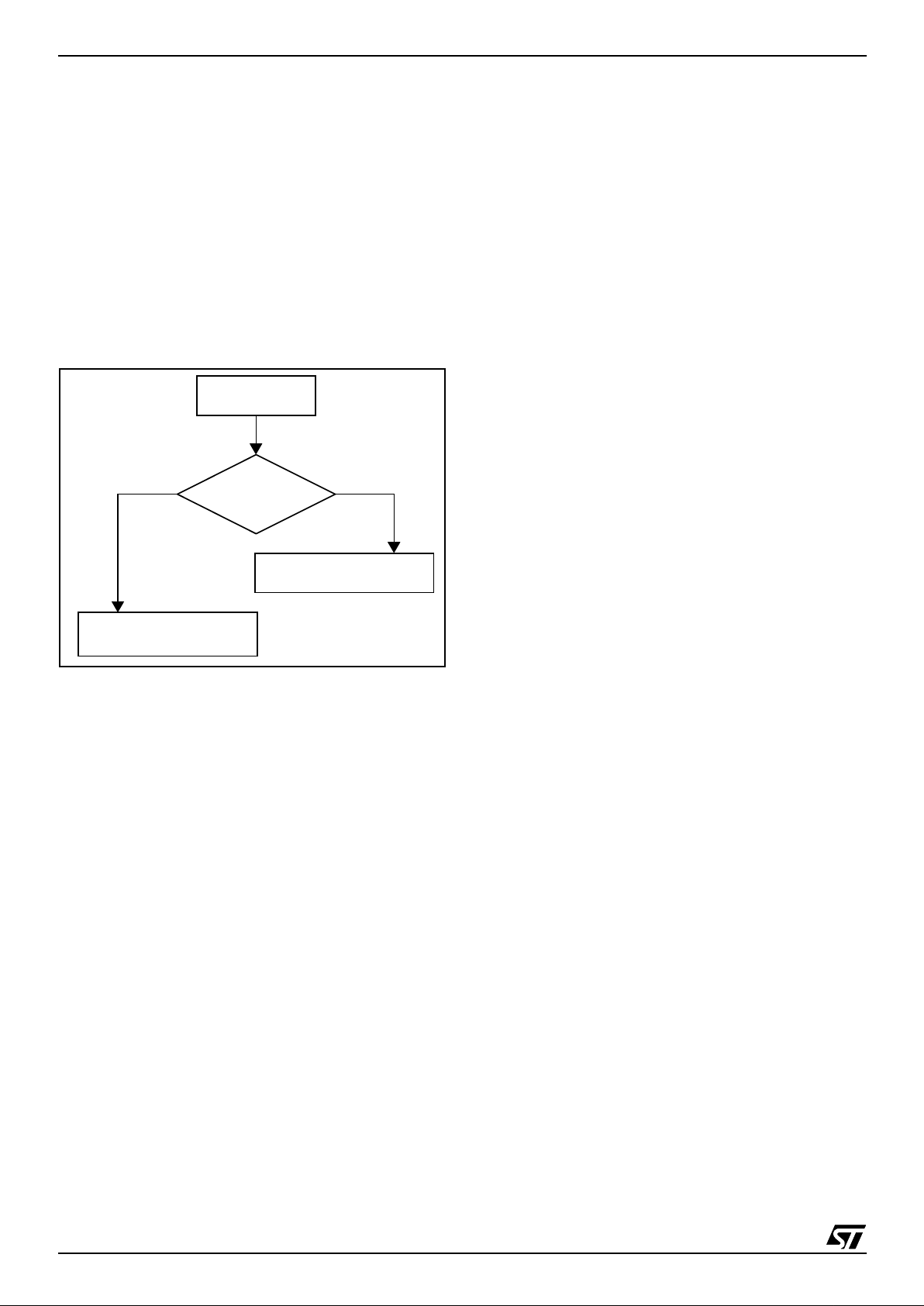
7.2 MASKING AND PROC ESSING FLOW
The interrupt masking is managed by the I1 and I0
bits of the CC register and the ISPRx registers
which give the interrupt software priority level of
each interrupt vector (see Table 5 ). The processing flow is shown in Fi gure 20.
When an interrupt request has to be serviced:
– Normal processing is suspended at the end of
the current instruction execution.
– The PC, X, A and CC registers are saved onto
the stack.
– I1 and I0 bits of CC register are set according to
the corresponding values in the ISPRx registers
of the serviced interrupt vector.
– The PC is then loaded with the interrupt vector of
the interrupt to service and the first instruction of
the interrupt service routine is fetched (refer to
“Interrupt Mapping” table for vector addresses).
The interrupt service routine should end with the
IRET instruction which c auses the contents of t he
saved registers to be recovered from the stack.
Note: As a cons equence of the IRET instruction,
the I1 and I0 bits will be restored from the stack
and the program in the previous level will resume.
Table 5. Interrupt Software Priority Levels
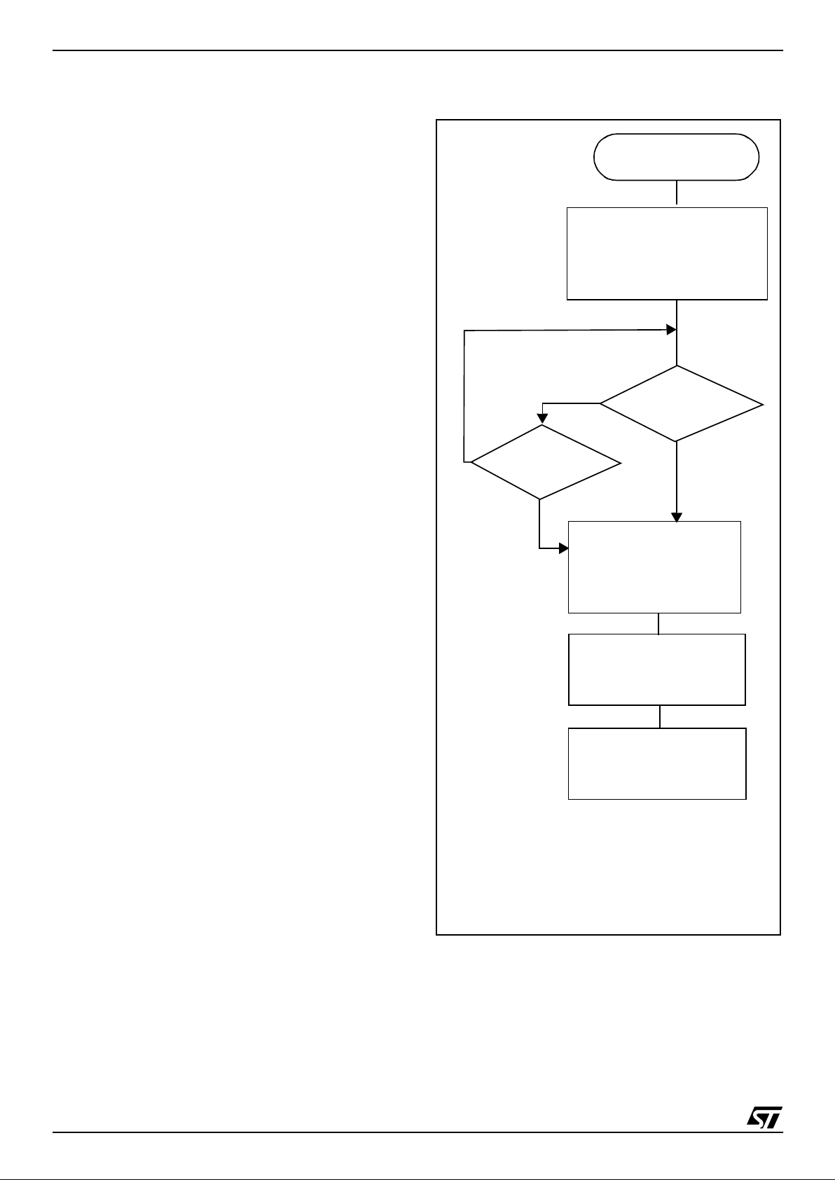
Figure 20. Int errupt Processing Flowchart
Interrupt software priority Le vel I1 I0
Level 0 (main) Low
High
10
Level 1 0 1
Level 2 0 0
Level 3 (= interrupt disable) 1 1
“IRET”
RESTORE PC, X, A, CC
STACK PC, X, A, CC
LOAD I1:0 FRO M INTER RUPT SW REG.
FETCH NEX T
RESET
TLI
PENDING
INSTRUCTION
I1:0
FROM STACK
LOAD PC FROM INTERRUPT VECTOR
Y
N
Y
N
Y
N
Interrupt has the same or a
lower software priority
THE INTERRUPT
STAYS PENDING
than c u rrent one
Interrupt has a higher
softwarepriority
than current one
EXECUTE
INSTRUCTION
INTERRUPT
ST7262
24/132
INTERRUPTS (Cont’d)
Servicing Pending In te rrupts
As several interrupts can b e pen ding at the s ame
time, the interrupt to be taken into account is determined by the following two-step process:
– the highest software priority interrupt is serviced,
– i f several interrupts have the same software pri-
ority then the interrupt with the highest hardware
priority is serviced first.
Figure 21 describes this decision process.
Figure 21. Priority Decision Process
When an interrupt request is not serviced immediately, it is latched and then processed when its
software priority combined with the hardware priority becomes the highest one.
Note 1: The hardware priority is exclusive while
the software one i s not. This allows the prev ious
process to succeed with only one interrupt.
Note 2: RESET, TRAP and TLI can be considered
as having the highest softwa re priority in the d ecision process.
Different Interrupt Vector Sources
Two interrupt source types are managed by the
CPU interrupt controller: the non-maskable type
(RESET, TLI, TRAP) and the maskable type (external or from internal peripherals).
Non-Maskable Sources
These sources are processed regardless of the
state of the I1 and I0 bits of the CC register (see
Figure 20). After stacking the PC, X, A and CC
registers (except for RESET), the corresponding
vector is loaded in the PC register and t he I1 and
I0 bits of the CC are set to disable interrupts (level
3). These sources allow the processor to exit
HALT mode.
■ TLI (Top Level Hardware Interrupt)
This hardware interrupt occurs when a specific
edge is detected on the dedicated TLI pin.
Caution: A TRAP instruction must not be used in a
TLI service routine.
■ TRAP (Non Maskable Software Interrupt)
This software interrupt is serviced when the TRAP
instruction is executed. It will be serviced according to the flowchart in Figure 20 as a TLI.
Caution: TRAP can be interrupted by a TLI.
■ RESET
The RESET source has the highe st priority in the
CPU. This means that the first current routine has
the highest software priority (level 3) and the highest hardware priority.
See the RESET chapter for more details.
Maskable Sources
Maskable interrup t vector sourc es can be servi ced
if the corresponding in terrupt is enabled and if its
own interrupt software priority (in ISPRx registers)
is higher than the one currently being serviced (I1
and I0 in CC register). If any of these two co nditions is false, the interrupt is la tched and thus remains pending.
■ External Interrupts
External interrupts allow the processor to exit from
HALT low power mode.
External interrupt sensitivity is software selectable
through the ITRFRE2 register.
External interrupt triggered on edge will be latched
and the interrupt request automatically cleared
upon entering the interrupt service routine.
If several input pins of a group connected to the
same interrupt line are selected simultaneously,
these w ill be log i cally NANDed.
■ Peripheral Interrupts
Usually the peripheral interrupts cause the Device
to exit from HALT mode except those mentioned in
the “Interrupt Mapping” table.
A peripheral interrupt occurs when a specific flag
is set in the peripheral status registers and if the
corresponding enable bit is set in the peripheral
control register.
The general sequence for clearing an interrupt is
based on an access to the status register followed
by a read or write to an associated register.
Note: The clearing sequence resets the internal
latch. A pending interrupt (i.e. waiting for being
serviced) will therefore be lost if the clear sequence is executed.
PENDING
SOFTWARE
Different
INTERRUPTS
Same
HIGHEST HARDWARE
PRIORITY SERVICED
PRIORITY
HIGHEST SOFTWARE
PRIORITY SERVICED
ST7262
25/132
INTERRUPTS (Cont’d)
7.3 INTERRUPTS AND LOW POWER MODES
All interrupts allow the processor to exit the WAIT
low power mode. On the contrary, only external
and other specified interrupt s allow the processor
to exit from the HALT modes (see column “Exit
from HALT” in “Interrupt Mapping” table). When
several pending interrupts are present whi le exiting HALT mode, the first one serviced can only be
an interrupt with e xit from HALT mode c apability
and it is selected through the same decision proc ess shown in Figure 21.
Note: If an interrupt, that is not able to Exit from
HALT mode, is pending with the highest priority
when exiting HALT mode, this interrupt is serviced
after the first one serviced.
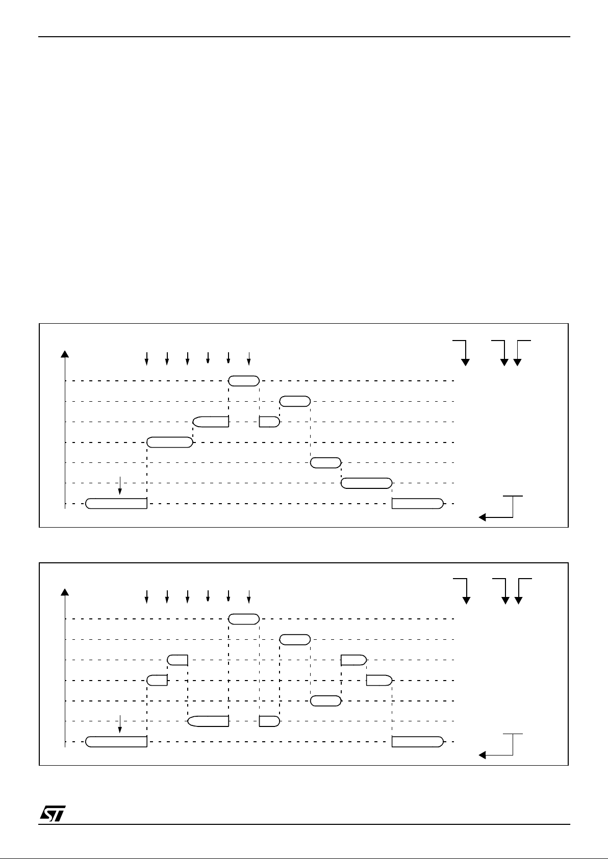
7.4 CONCURRENT & NESTED MANAGEMENT
The following Figure 22 and Figure 23 show two
different interrupt management modes. The first is
called concurrent mode and do es not allow an interrupt to be interrupted, unlike the nested mode in
Figure 23. The interrupt hardware priority is given
in this order from the l owes t to the hi ghest: M A IN,
IT4, IT3 , IT2, IT1, IT0, TLI. The software priority is
given for each interrupt.
Warning: A stack overflow may occur without notifying the software of the failure.
Figure 22. Concurrent Interru pt Manage m ent
Figure 23. Nested Interrupt Management
MAIN
IT4
IT2
IT1
TLI
IT1
MAIN
IT0
I1
HARDWARE PRIORITY
SOFTWARE
3
3
3
3
3
3/0
3
11
11
11
11
11
11 / 10
11
RIM
IT2
IT1
IT4
TLI
IT3
IT0
IT3
I0
10
PRIORITY
LEVEL
USED STACK = 10 BYTES
MAIN
IT2
TLI
MAIN
IT0
IT2
IT1
IT4
TLI
IT3
IT0
HARDWARE PRIORITY
3
2
1
3
3
3/0
3
11
00
01
11
11
11
RIM
IT1
IT4
IT4
IT1
IT2
IT3
I1 I0
11 / 10
10
SOFTWARE
PRIORITY
LEVEL
USED STACK = 20 BYTES
ST7262
26/132
INTERRUPTS (Cont’d)
7.5 INTERRUPT REGISTER DESCRIPTION
CPU CC REGISTER INTERRUPT BITS
Read/Write
Reset Value: 111x 1010 (xAh)
Bit 5, 3 = I1, I0
Soft w a re In te r rupt Prio rity
These two bits indicate the current interrupt software priority.
These two bits are set/cle ared by hardware whe n
entering in interrupt. The loaded value is given by
the corresponding bits in the interrupt software priority registers (ISPRx).
They can be also s et/cleared by s oft ware wi th the
RIM, SIM, HALT, WFI, IRET and PUSH/POP instructions (see “Interrupt Dedicated Instruction
Set” table).
*Note: TLI, TRAP and RESET events ca n in terru pt
a level 3 program.
INTERRUPT SOFTWARE PRIORITY REGISTERS (ISPRX)
Read/Write (bit 7:4 of ISPR3 are read only)
Reset Value: 1111 1111 (FFh)
These four registers contain the interrupt software
priority of each interrupt vector.
– Each interrupt vector (except RESET and TRAP)
has corresponding bits in these registers where
its own software priority is stored. This correspondance is shown in the following table.
– Each I1_x and I0_x bit value in the ISPRx regis-
ters has the same meaning as the I1 and I0 bits
in the CC register.
– Level 0 can not be written (I1_x=1, I0_x=0). In
this case, the previously stored value is kept. (example: previous=CFh, write=64h, result=44h)
The RESET, TRAP a nd TLI vectors have no s oftware priorities. When one is serviced, the I1 and I0
bits of the CC register are both set.
*Note: Bits in the ISPRx registers which correspond to the TLI can be read and written but they
are not significant in the interrupt process management.
Caution: If the I1_x and I0_x bits are modified
while the interrupt x is execu ted the following behaviour has to be considered: If the interrupt x is
still pending (new interrupt or flag not cleared) and
the new software priority is highe r than the previous one, the interrupt x is re-ent ered. Otherwise,
the software priority stays unchanged up to the
next interrupt request (after the IRET of the interrupt x).
70
11I1 H I0 NZC
Interrupt Software Priority Level I1 I0
Level 0 (main)
Low
High
10
Level 1 0 1
Level 2 0 0
Level 3 (= interrupt disable*) 1 1
70
ISPR0 I1_3 I0_3 I1_2 I0_2 I1_1 I0_1 I1_0 I0_0
ISPR1 I1_7 I0_7 I1_6 I0_6 I1_5 I0_5 I1_4 I0_4
ISPR2 I1_11 I0_11 I1_10 I0_10 I1_9 I0_9 I1_8 I0_8
ISPR3 1 1 1 1 I1_13 I0_13 I1_12 I0_12
Vector address ISPRx bits
FFFBh-FFFAh I1_0 and I0_0 bits*
FFF9h-FFF8h I1_1 and I0_1 bits
... ...
FFE1h-FFE0h I1_13 and I0_13 bits
ST7262
27/132
7.6 Interrupt Register
INTERRUPT REGISTER 1 (ITRFRE1)
Address: 0008h - Read/Write
Reset Value: 0000 0000 (00h)
Bit 7:0 = ITiE
Interrupt Enable
0: I/O pin free for general purpose I/O
1: ITi external interrupt enabled.
Note: The corresponding interrupt is generated
when:
– a rising edge occurs on the IT5/IT6 pins
– a falling edge occurs on the IT1, 2, 3, 4, 7 and 8
pins
INTERRUPT REGISTER 2 (ITRFRE2)
Address: 0039h - Read/Write
Reset Value: 0000 0000 (00h)
Bit 7:6 = CTL[3:2]
IT[12:11] Interrupt Sensitivity
These bits are set and cleared by software. They
are used to configure the edge and level sensitivity
of the IT12 and IT11 external interrupt pins (this
means that both must have the same sensitivity).
Bit 5:4 = CTL[1:0]
IT[10:9]1nterrupt Sensitivity
These bits are set and cleared by software. They
are used to configure the edge and level sensitivity
of the IT10 and IT9 external interrupt pins (this
means that both must have the same sensitivity).
Bit 3:0 = ITiE
Interrupt Enable
0: I/O pin free for general purpose I/O
1: ITi external interrupt enabled.
70
IT8E IT7E IT6E IT5E IT4E IT 3E IT2E IT1E
70
CTL3 CTL2 CTL1 CTL0 IT12E IT11E IT10E IT9E
CTL3 CTL2 IT[12:11] Sensitivity
0 0 Falling edge and low level
0 1 Rising edge only
1 0 Falling edge only
1 1 Rising and falling edge
CTL1 CTL0 IT[10:9] Sensitivity
0 0 Falling edge and low level
0 1 Rising edge only
1 0 Falling edge only
1 1 Rising and falling edge

ST7262
28/132
INTERRUPTS (Cont’d)
Table 6. I nte rrupt Mapping
Table 7. Nested Interrupts Register Map and Reset Values
N°
Source
Block
Description
Register
Label
Priority
Order
Exit
from
HALT
Address
Vector
Reset
Highest
Priority
Lowest
Priority
Yes FFFEh-FFFFh
TRAP software interrupt No FFFCh-FFFDh
0 ICP FLASH Start programming NMI interrupt Yes FFFAh-FFFBh
1 USB USB End Suspend interrupt USBISTR Yes FFF8h-FFF9h
2
I/O Ports
Port A external interrupts IT[4:1] ITRFRE1 Yes FFF6h-FFF7h
3 Port B external interrupts IT[8:5] ITRFRE1 Yes FFF4h-FFF5h
4 Port C external interrupts IT[12:9] ITRFRE2 Yes FFF2h-FFF3h
5 TBU Timebase Unit interrupt TBUCSR No FFF0h-FFF1h
6 ART ART/PWM Timer interrupt ICCSR Yes FFEEh-FFEFh
7 SPI SPI interr upt vector SPISR Yes FFECh-FFEDh
8 SC I SCI interrupt vector SCISR No FFEAh-FFEBh
9 USB USB interrupt vector USBISTR No FFE8h-FFE9h
10 ADC A/D End of conversion interrupt ADCCSR No FFE6h-FFE7h
Reserved area FFE0h-FFE5h
Address
(Hex.)
Register
Label
76543210
0032h
ISPR0
Reset Value
Ext. Interrupt Port B Ext. Interrupt Port A USB END SUSP Not Used
I1_3
1
I0_3
1
I1_2
1
I0_2
1
I1_1
1
I0_1
111
0033h
ISPR1
Reset Value
SPI ART TBU Ext. Interrupt Port C
I1_7
1
I0_7
1
I1_6
1
I0_6
1
I1_5
1
I0_5
1
I1_4
1
I0_4
1
0034h
ISPR2
Reset Value
Not Used ADC USB SCI
I1_11
1
I0_11
1
I1_10
1
I0_10
1
I1_9
1
I0_9
1
I1_8
1
I0_8
1
0035h
ISPR3
Reset Value1111
Not Used Not Used
I1_13
1
I0_13
1
I1_12
1
I0_12
1

ST7262
29/132
8 POWER SAVING MODES
8.1 INTRODUCTION
There are three Power Saving modes. Slow Mode
is selected by setting the SMS bits in the Miscellaneous register. Wait and Halt modes may be entered using the WFI and HALT instructions.
After a RESET the normal operat ing mode is selected by default (RUN mode). This mode drives
the device (CPU and embedded peripherals) by
means of a master clock which is based on the
main oscillator f re quency divided by 3 and multiplied by 2 (f
CPU
).
From Run mode, the different power saving
modes may be selected by setting the relevant
register bits or by calling the specific ST7 software
instruction whose action depends on the oscillator
status.
8.1.1 Slow Mode
In Slow mode, the osc illator frequency can be d ivided by a value defined in the Miscellaneous
Register. The CPU and peripherals are clocked at
this lower frequency. Slow mode is used to reduce
power consumption, and enables the user to adapt
clock frequency to available supply voltage.
8.2 WAIT MODE
WAIT mode places the MCU in a low power c onsumption mode by stopping the CPU.
This pow e r s a v ing mo de is se lected b y ca llin g the
“WFI” ST7 software instruction.
All peripherals remain active. During WAIT mode,
the I bit of the CC register is forced to 0, to enable
all interrupts. All other registers and memory remain unchanged. The MCU remains in WAIT
mode until an interrupt or Res et oc curs, where upon the Program Counter branches to the starting
address of the interrupt or Reset service routine.
The MCU w ill re mai n in W AIT mo de unt il a Res et
or an Interrupt occurs, causing it to wake up.
Refer to Figure 24.
Figure 24. WAIT Mode Flow Chart
WFI INSTRUCTION
RESET
INTERRUPT
Y
N
N
Y
CPU CLOCK
OSCILLATOR
PERIPH. CLOCK
I-BIT
ON
ON
CLEARED
OFF
CPU CLOCK
OSCILLATOR
PERIPH. CLOCK
I-BIT
ON
ON
SET
ON
FETCH RESET VECTOR
OR SERVICE INTERRUPT
514 CPU CLOCK
CYCLES DELAY
IF RESET
Note: Before servicing an interrupt, the CC register is
pushed on the sta ck. The I-Bit is s et d uring the inte rrupt routine and cleared when the CC register is
popped.
ST7262
30/132
POWER SAVING MODES (Cont’d)
8.3 HALT MODE
The HALT mode is the MCU lowest power consumption mode. The HALT mode is entered by executing the HALT instruction. The internal oscillator is then turned off, causing all internal processing to be stopped, including the operation of the
on-chip peripherals.
When entering HALT mode, the I bit in the Condition Code Register is cleared. Thus, any of the external interrupts (ITi or US B end suspend mode),
are allowed and if an interrupt occurs, the CPU
clock becomes active.
The MCU can e xit HAL T mode on reception of either an external interrupt on ITi, an end suspen d
mode interrupt coming from USB peripheral, or a
reset. The osc illato r is t hen t ur ned on and a stabilization time is provided before rele as ing CPU operation. The stabilization time is 514 CPU clock cycles.
After the start up delay, the CPU continues operation by servicing the interrupt which wakes it up or
by fetching the reset vector if a reset wakes it up.
Figure 25. HALT Mod e Flo w C ha r t
N
N
EXTERNAL
INTERRUPT*
RESET
HALT INSTRUCTION
514 CPU CLOCK
FETCH RESET VECTOR
OR SERVICE INTERRUPT
CYCLES DELAY
CPU CLOCK
OSCILLATOR
PERIPH. CLOCK
I-BIT
ON
ON
SET
ON
CPU CLOCK
OSCILLATOR
PERIPH. CLOCK
I-BIT
OFF
OFF
CLEARED
OFF
Y
Y
Note: Before servicing an interrupt, the CC register is
pushed on the stac k. T he I -Bit i s se t du ring the interrupt routine and cleared when the CC register is
popped.

ST7262
31/132
9 I/O PORTS
9.1 INTRODUCTION
The I/O ports offer different functional modes:
transfer of data through digital inputs and outputs
and for specific pins:
– Analog signal input (ADC)
– Alternate signal input/out put for the on-chip pe-
ripherals.
– External interrupt generation
An I/O port i s c om posed of up to 8 pins. Each pi n
can be programmed independently as digital input
or digital output.
9.2 FUNCTIONAL DESCRIPTION
Each port is associated with 2 main registers:
– Data Register (DR)
– Data Direction Register (DDR)
Each I/O pin may be programmed using the corre-
sponding register bits in DDR regi ster: bi t x corresponding to pin x of the port. The same correspondence is used for the DR register.
Table 8. I /O Pi n Fu nc ti ons
9.2.1 Input Modes
The input configuration is s ele cted by clearing the
corresponding DDR register bit.
In this case, reading the DR register returns the
digital value applied to the external I/O pin.
Notes:
1. All the inputs are triggered by a Schmitt trigger.
2. When switching from input mode to output
mode, the DR reg ister should be writte n first to
output the correct value as s oon as the port is
configured as an output.
Interrupt function
When an external interrupt function of an I/O pin, is
enabled using the ITFRE registers, an event on
this I/O can generate an external Interrupt request
to the CPU. The i nterrupt sensitivit y is programma-
ble, the options are given in the description of the
ITRFRE interrupt registers.
Each pin can independently generate an I nterrupt
request.
Each external interrupt vecto r is linked to a dedicated group of I/O port pins (see Interrupts section). If more than one input pin is selected sim ultaneously as interrupt source, this is logically ANDed and inverted. For this reason, if an event occurs on one of the i nterrupt pins, it masks t he other
ones.
9.2.2 Output Mode
The pin is configured in output mode by setting the
corresponding DDR register bit (see Table 7).
In this mode, writing “0” or “1” to the DR register
applies this digital value to the I/O pin throu gh the
latch. Then reading the DR register returns the
previously stored value.
Note: In thi s mo de, th e interrupt function is disabled.
9.2.3 Alternate Functions
Digital A lternate Fu nct i on s
When an on-chip peripheral is configured to use a
pin, the alternate function is au tomatically selected. This alternate function takes priority over
standard I/O programming. When the signal is
coming from an on-chip peripheral, the I/O pin is
automatically configured in output mode (push-pull
or open drain according to the peripheral).
When the signal is goi ng t o an on-c hip pe ripheral,
the I/O pin ha s to be configured in input m ode. In
this case, the pin state is also digitally readable by
addressing the DR register.
Notes:
1. Input pull-up conf iguration can cause a n unexpected value at the alternate peripheral input.
2. When the on-chip peripheral uses a pin as input
and output, this pin must be configured as an
input (DDR = 0).
Warning
: Alternate functions of peripherals must
must not be activated when the external interrupts
are enabled on the same pin, in order to avoid
generating spurious interrupts.
DDR MODE
0 Input
1 Output

ST7262
32/132
I/O PORTS (Cont’d)
Analog Alternate Functions
When the pin is used as an ADC input, the I/O
must be configured as input. The analog multiplexer (controlled by the ADC regi sters) switches the
analog voltage present o n the selected pin to th e
common analog rail which is connected to the
ADC input.
It is recommended not to change the voltage level
or loading on any port pin while conversion is in
progress. Furthermore it is recommended not to
have clocking pins located c lose to a selected analog pin.
Warning
: The analog input voltage level must be
within the limits s tated in the A bsolute Ma ximum
Ratings.
9.2.4 I/O Port Implementation
The hardware implementation on each I/O port depends on the settings in the DDR register and specific features of the I/O port such as ADC Input or
true open drain.

ST7262
33/132
I/O PORTS (Cont’d)
9.2.5 Port A
Table 9. Port A Description
Figure 26. PA[7:0] Configuration
PORT A
I/O Alternate Function
Input* Output Signal Condition
PA0 floating push-pull
USBOE USBOE = 1 (MISC)
IT1 Schmitt triggered input IT1E = 1 (ITRFRE1)
AIN0 (ADC) CS[2:0] = 000 (ADCCSR)
PA1 floating push-pull
IT2 Schmitt triggered input IT2E = 1 (ITRFRE1)
AIN1 (ADC) CS[2:0] = 001 (ADCCSR)
PA2 floating push-pull
IT3 Schmitt triggered input IT3E = 1 (ITRFRE1)
AIN2 (ADC) CS[2:0] = 010 (ADCCSR)
PA3 floating push-pull
IT4 Schmitt triggered input IT4E = 1 (ITRFRE1)
AIN3 (ADC) CS[2:0] = 011 (ADCCSR)
PA4 floating push-pull AIN4 (ADC) CS[2:0] = 100 (ADCCSR)
PA5 floating push-pull AIN5 (ADC) CS[2:0] = 101 (ADCCSR)
PA6 floating push-pull AIN6 (ADC) CS[2:0] = 110 (ADCCSR)
PA7 floating push-pull AIN7 (ADC) CS[2:0] = 111 (ADCCSR)
*Reset State
DR
DDR
LATCH
LATCH
DR SEL
DDR SEL
V
DD
PAD
ANALOG
SWITCH
ANALOG ENABLE
(ADC)
ALTERNATE ENABLE
ALTERNATE ENABLE
DIGITA L EN AB L E
ALTE RN AT E ENABL E
ALTER NAT E
ALTERN AT E INPUT
OUTPUT
P-BUFFER
N-BU FF E R
1
0
1
0
V
SS
DATA BUS
COMMON ANALOG RAIL
V
DD
DIODES

ST7262
34/132
I/O PORTS (Cont’d)
9.2.6 Port B
Table 10. Port B Description
Figure 27. Port B and Port C [7:2] Configuration
PORT B
I/O Alternate Function
Input* Output Signal Condition
PB0 floating push-pull (high sink) MCO (Main Clock Output) MCO = 1 (MISCR)
PB1 floating push-pull (high sink) RDI SCI enabled
PB2 floating push-pull (high sink) TDO TE = 1 (SCICR2)
PB3 floating push-pull (high sink) ARTCLK EXCL = 1 (ARTCSR)
PB4 floating push-pull (high sink)
ARTIC1 ART Timer enabled
IT5 Schmitt triggered input IT5E = 1 (ITRFRE1)
PB5 floating push-pull (high sink)
ARTIC2 ART Timer enabled
IT6 Schmitt triggered input IT6E = 1 (ITRFRE1)
PB6 floating push-pull (high sink)
PWM1 OE0 = 1 (PWMCR)
IT7 Schmitt triggered input IT7E = 1 (ITRFRE1)
PB7 floating push-pull (high sink)
PWM2 OE1 = 1 (PWMCR)
IT8 Schmitt triggered input IT8E = 1 (ITRFRE1)
*Reset State
DR
DDR
LATCH
LATCH
DR SEL
DDR SEL
V
DD
PAD
ALTERNATE ENABLE
ALTERNATE ENABLE
ALTERNATE ENABLE
ALTERNATE
ALTERNATE INPUT
OUTPUT
P-BUFFER
N-BUFFER
1
0
1
0
CMOS SCHMITT TRIGGER
V
SS
V
DD
DIODES
DATA BUS
PULL-UP*
* PULL-UP ON PORT C [7:2] ONLY

ST7262
35/132
I/O PORTS (Cont’d)
9.2.7 Port C
Table 11. Port C Description
Figure 28. Port C[1:0] Configuration
PORT C
I/O Alternate Function
Input* Output Signal Condition
PC0 floating true open drain
PC1 floating true open drain
PC2 with pull-up push-pull IT9 Schmitt triggered input IT9E = 1 (ITRFRE2)
PC3 with pull-up push-pull
SCK SPI enabled
IT10 Schmitt triggered input IT10E = 1 (ITRFRE2)
PC4 with pull-up push-pull
SS
SPI enabled
IT11 Schmitt triggered input IT11E = 1 (ITRFRE2)
PC5 with pull-up push-pull
MISO SPI enabled
IT12 Schmitt triggered input IT12E = 1 (ITRFRE2)
PC6 with pull-up push-pull MOSI SPI enabled
PC7 with pull-up push-pull
*Reset State
DR
DDR
LATCH
LATCH
DR SEL
DDR SEL
PAD
ALTERNATE ENABLE
ALTERNATE ENABLE
ALTERNATE
OUTPUT
N-BUFFER
1
0
1
0
CMOS SCHMITT TRIGGER
V
SS
DIODES
DATA BUS

ST7262
36/132
I/O PORTS (Cont’d)
9.2.8 Port D
Table 12. Port D Description
Figure 29. P ort D C onfi guration
PORT D
I/O Alternate Function
Input* Output Signal Condition
PD0 with pull-up push-pull
PD1 with pull-up push-pull
PD2 with pull-up push-pull
PD3 with pull-up push-pull
PD4 with pull-up push-pull
PD5 with pull-up push-pull
PD6 with pull-up push-pull
*Reset State
DR
DDR
LATCH
LATCH
DR SEL
DDR SEL
V
DD
PAD
ALTE RN AT E ENABL E
ALTERNATE ENABLE
ALTERNATE ENABLE
ALTERNATE
ALTERNATE INPUT
PULL-UP
OUTPUT
P-BUFFER
N-BUFFER
1
0
1
0
CMOS SCHMITT TRIG GER
V
SS
V
DD
DATA BUS
DIODES

ST7262
37/132
I/O P O R TS (Cont’d)
9.2.9 Register Description
DATA REGISTER (DR)
Port x Data Register
PxDR with x = A, B, C or D.
Read/Write
Reset Value: 0000 0000 (00h)
Bits 7:0 = D[7:0]
Data register 8 bits.
The DR register has a specific behaviour according to the selected input/output configuration. Writing the DR register is always taken into account
even if the pin is configured as an input; this allows
to always have the expected level on the pin when
toggling to output mode. Reading the DR register
returns either the DR register latch content (pin
configured as output) or the digital value applied to
th e I /O pin (pin configure d as input).
DATA DIRECTION REGISTER (DDR)
Port x Data Direction Register
PxDDR with x = A, B, C or D.
Read/Write
Reset Value: 0000 0000 (00h)
Bits 7:0 = DD[7:0]
Data direction register 8 bits.
The DDR reg ister gives the i nput/output direction
configuration of the pins. Each bit is set and
cleared by software.
0: Input mode
1: Output mode
70
D7 D6 D5 D4 D3 D2 D1 D0
70
DD7 DD6 DD5 DD4 DD3 DD2 DD1 DD0

ST7262
38/132
I/O PORTS (Cont’d)
Table 13. I/O Port Register Map and Reset Values
Address
(Hex.)
Register
Label
76543210
Reset Value
of all I/O port registers
00000000
0000h PADR
MSB LSB
0001h PADDR
0002h PBDR
MSB LSB
0003h PBDDR
0004h PCDR
MSB LSB
0005h PCDDR
0006h PDDR
MSB LSB
0007h PDDDR

ST7262
39/132
9.3 MISC EL LA NEOUS REGISTER
MISCELL ANE OUS REG ISTER
Read Write
Reset Value - 0000 0000 (00h)
Bits 7:4 = Reserved
Bits 3:2 = SMS[1:0]
Slow Mod e Selection
These bits select the Slow Mode frequency (depending on the oscillator frequen cy confi gured by
option byte).
Bit 1 = USBOE
USB Output Enable
0: PA0 port free for general purpose I/O
1: USBOE alternate function enabled. The USB
output enable signal is output on the PA0 port
(at “1” when the ST7 USB is transmitting data).
Bit 0 = MCO
Main Clock Out
0: PB0 port free for general purpose I/O
1: MCO alternate function enabled (f
CPU
output on
PB0 I/O port)
70
- - - - SMS1 SMS0
US-
BOE
MCO
OSC12/6 SMS1 SMS0
Slow Mode Frequency
(MHz.)
f
OSC
= 6 MHz.
00 4
01 2
10 1
1 1 0.5
f
OSC
= 12 MHz.
00 8
01 4
10 2
11 1

ST7262
40/132
10 ON-CHIP PER IPHERALS
10.1 WATCHDOG TIMER (WDG)
10.1.1 Introduction
The Watchdog t imer is used to d etect the occurrence of a software fault, usually generated by external interference or by unforeseen logical conditions, which causes the application program to
abandon its normal seque nce. The W atchdog circuit generates an MCU reset o n expiry of a programmed time period, unless the program refresh-
es the counter’s contents before the T6 bit becomes cleared.
10.1.2 Main Features
■ Programmable free-running downcounter (64
increments of 65536 CPU cycles)
■ Programmable reset
■ Reset (if watchdog activated) when the T6 bit
reaches zero
■ Hardware Watchdog selectable by option byte
10.1.3 Functional Description
The counter value stored in the CR register (bits
T[6:0]), is decremented every 65,536 mach ine cycles, and the length of the timeout period can b e
programmed by the user in 64 increments.
If the watchdog is activated (the WDGA bit is set)
and when the 7-bit timer (bits T[6:0]) rolls over
from 40h to 3Fh (T6 becom es cleared ), it initiates
a reset cycle pulling low the reset p in for typ ically
500ns.
The application program must write in the CR register at regular intervals during normal operation to
prevent an MCU reset. This downcounter is freerunning: it counts down even if the watchdog is diabled The value to be stored in the CR register
must be between FFh and C0h (see Table 14):
– The WDGA bit is set (watchdog enabled)
– The T6 bit is set to prevent generating an imme-
diate reset
– The T[5:0] bits contain the number of increments
which represents the time delay before the
watchdog produces a reset.
Table 14.Watchdog Timing (f
CPU
= 8 MHz)
Figure 30. Watchd og Block Diag ram
CR Register
initial value
WDG timeout period
(ms)
Max FFh 524.288
Min C0h 8.192
RESET
WDGA
7-BIT DOWNCOU NTE R
f
CPU
T6 T0
CLOCK DIVIDER
WATCHDOG CONTROL REGISTER (CR)
÷
65536
T1
T2
T3
T4
T5

ST7262
41/132
WATCH DOG TI MER (Cont’d)
10.1.4 Software Watchdog Option
If Software Watchdog is selected by option byte,
the watchdog is disabled following a reset. O nce
activated it cannot be disabled, except by a reset.
The T6 bit can be used t o generate a s of tw are reset (the WDGA bit is set and the T6 bit is cleared).
10.1.5 Hardware Watchdog Option
If Hardware Watchdog is selected by o ption byte,
the watchdog is always active and the WDGA bit in
the CR is not used.
10.1.6 Low Power Mo des
WAIT Instruction
No effect on Watchdog.
HALT Instruction
Halt mode can be us ed when the watchdo g is enabled. When the oscillator is stopped, the WDG
stops counting and is no longer able to generate a
reset until the microcontroller receives an external
interrupt or a reset.
If an external interrupt is received, the WDG restarts counting after 514 CPU clocks. In the case
of the Software Watchdog option, if a reset is generated, the WDG is disabled (reset state).
Recommendations
– Make sure that an external event is available to
wake up the microcontroller from Halt mode.
– Before executing the HALT instruction, refresh
the WDG counter, to avoid an unexpected WDG
reset immediately after waking up the microcontroller.
– When using an external interrupt to wake up t he
microcontroller, reinitialize the corresponding I/O
as Input before executing the HALT instruction.
The main reason for this is that the I/O may be
wrongly configured due to external interference
or by an unforeseen logical condition.
– The opcode for the HALT instruction is 0x8E. To
avoid an unexpected HALT instruction due to a
program counter failure, it is advised to clear all
occurrences of the data value 0x8E from memory. For example, avoid defining a constant in
ROM with the value 0x8E.
– As the HALT instruction clears the I bit in the CC
register to allow interrupts, the user may choose
to clear all pending interrupt bits before executing the HALT instruction. This avoids entering
other peripheral interrupt routines after executing
the external interrupt routine corresponding to
the wake-up event (reset or external interrupt).
10.1.7 Interrupts
None.
10.1.8 Register Desc4ription
CONTROL REGISTER (CR)
Read/Write
Reset Value: 0111 1111 (7Fh)
Bit 7 = WDGA
Activation bit
.
This bit is set by software and only cleared by
hardware after a reset. When WDGA = 1, the
watchdog can generate a reset.
0: Watchdog disabled
1: Watchdog enabled
Note: This bit is not used if the hardware watchdog option is enabled by option byte.
Bits 6:0 = T[6:0]
7-bit tim er (M SB to LSB) .
These bits contain the decremented value. A reset
is produced when it rolls over from 40h to 3Fh (T6
becomes cleared).
Table 15. Watchdog Time r Register Map and Rese t Values
70
WDGA T6 T5 T4 T3 T2 T1 T0
Address
(Hex.)
Register
Label
76543210
0Dh
WDGCR
Reset Value
WDGA
0
T6
1
T5
1
T4
1
T3
1
T2
1
T1
1
T0
1

ST7262
42/132
10.2 PWM AUTO-RELOAD TIMER (ART)
10.2.1 Introduction
The Pulse Width Modulated Auto-Reload Timer
on-chip peripheral consists of an 8-bit auto reload
counter with compare/capture capabilities and of a
7-bit prescaler clock source.
These resources allow five possible operating
modes:
– Generation of up to 4 independent PWM signals
– Output compare and Time base interrupt
– Up to two input capture functions
– External event detector
– Up to two external interrupt sources
The three first modes can be used together with a
single counter frequency.
The timer can b e used t o wake up the MCU from
WAIT and HALT modes.
Figure 31. PWM Auto-Reload Timer Block Diagram
OVFINTERRUPT
EXCL CC2 CC1 CC0 TCE FCRL OIE OVF
ARTCSR
f
INPUT
PWMx
PORT
FUNCTION
ALTERNATE
OCRx
COMPARE
REGISTER
PROGRAMMABLE
PRESCALER
8-BIT COUNTER
(ARTCAR REGISTER)
ARTARR
REGISTER
ARTICRx
REGISTER
LOAD
OPx
POLARITY
CONTROL
OEx
PWMCR
MUX
f
CPU
PWMDCRx
REGISTER
LOAD
f
COUNTER
ARTCLK
f
EXT
ARTICx
ICFxICSx
ARTICCSR
LOAD
ICx INTERRUPT
ICIEx
INPUT CAPTURE
CONTROL

ST7262
43/132
PWM AUTO-RELOAD TIMER (Cont’d)
10.2.2 Functional Description
Counter
The free running 8-bi t cou nter is f ed by the output
of the prescaler, and is incremented on every rising edge of the clock signal.
It is possible to read or write the cont ents of the
counter on the fly by reading or writing the Counter
Access register (ARTCAR).
When a counter overflow occurs, the counter is
automatically reloaded with the contents of the
ARTARR register (the prescaler is not affected).
Counter clock and prescaler
The counter clock frequency is given by:
f
COUNTER
= f
INPUT
/ 2
CC[2:0]
The timer counter’s input clock (f
INPUT
) feeds the
7-bit programmable prescaler, which selects one
of the 8 available taps of the prescaler, as defined
by CC[2:0] bits in the Control/Status Register
(ARTCSR). Thus the division factor of the prescaler can be set to 2
n
(where n = 0, 1,..7).
This f
INPUT
frequency source is selected through
the EXCL bit of the ARTCSR register and can be
either the f
CPU
or an external input frequency f
EXT
.
The clock input to the counter is enabled by the
TCE (Timer Counter Enable) bit in the ARTCSR
register. When TCE is reset, the counter is
stopped and the prescaler and counter contents
are frozen. When T CE is set, the coun ter runs at
the rate of the selected clock so ur ce.
Counter and Prescaler Initialization
After RESET, the counter and the prescaler are
cleared and f
INPUT
= f
CPU
.
The counter can be initialized by:
– Writing to the ARTARR register and then setting
the FCRL (Force Counter Re-Load) and the TCE
(Timer Counter Enable) bits in the ARTCSR reg-
ister.
– Writing to the ARTCAR counter access register,
In both cases the 7-b it prescaler is also cleared,
whereupon counting will start from a known value.
Direct access to the prescaler i s not possi ble .
Output compare control
The timer compare function is based on four different comparisons with the counter (one for each
PWMx output). Each comparison is made between the counter value and an output compare
register (OCRx) value. This OCRx register can not
be accessed directly, it is loaded from the duty cycle register (PWMDCRx) at each overflow of the
counter.
This double buffering method avoids glitch generation when changing the duty cycle on the fly.
Figure 32. Output compare control
COUNTER
FDh FEh FFh FDh FEh FFh FDh FEh
ARTARR=FDh
f
COUNTER
OCRx
PWMDCRx
FDh
FEh
FDh
FEh
FFh
PWMx

ST7262
44/132
PWM AUTO-RELOAD TIMER (Cont’d)
Independent PWM signal generation
This mode allows up to four Pulse W idth Mo dulated signals to be generated on the PWMx output
pins with minimum core processing overhead.
This function is stopped during HALT mode.
Each PWMx ou tput signal can be sel ected independently using the corresponding OEx bit in the
PWM Control register (PWMCR). When this bit is
set, the corresponding I/O pin is configured as output push-pull alternate function.
The PWM signals all have the same frequency
which is controlled by the counter period and the
ARTARR register value.
f
PWM
= f
COUNTER
/ (256 - ARTARR)
When a counter overflow occurs, the PWMx pin
level is changed depending on the corresponding
OPx (output polarity) bit in the P WMCR register.
When the counter reaches the value contained in
one of the output compare register (OCRx) the
corresponding PWMx pin level is restored.
It should be noted that the reload values wil l also
affect the value and the resoluti on of the duty cycl e
of the PWM out put sign al. T o obtain a signal on a
PWMx pin, the contents of the OCRx register must
be greater than the con tents of the A RTARR register.
The maximum av ailable resolution for the PW Mx
duty cycle is:
Resolution = 1 / (256 - ARTARR)
Note: To get the maximum resolution (1/256), the
ARTARR register must be 0. With this maxi mum
resolution, 0% and 100% can be obtained by
changing the polarity.
Figure 33. PWM Auto-reload Timer Function
DUTY CYCLE
REGISTER
AUTO-RELOAD
REGISTER
PWMx OUTPUT
t
255
000
WITH OEx=1
AND OPx=0
(ARTARR)
(PWMDCRx)
WITH OEx=1
AND OPx=1
COUNT ER

ST7262
45/132
Figure 34. PWM Signal from 0% to 100% Duty Cycle
COUNTER
PWMx OUTPUT
t
WITH OEx=1
AND OPx=0
FDh FEh FFh FDh FEh FFh FDh FEh
OCRx=FCh
OCRx=FDh
OCRx=FEh
OCRx=FFh
ARTARR=FDh
f
COUNTER

ST7262
46/132
PWM AUTO-RELOAD TIMER (Cont’d)
Output compare and Tim e base interru pt
On overflow, the OVF flag of the ARTCSR register
is set and an overflow interrupt request is generated if the overflow interrupt enable bit, OIE, in the
ARTCSR register, is set. The OVF flag must be reset by the user software. This interrupt can be
used as a time base in the application.
External clock and event detector mode
Using the f
EXT
external prescaler input clock, the
auto-reload timer can be used as an external clock
event detector. In this mode, the ARTARR register
is used to select the n
EVENT
number of even ts to
be counted before setting the OVF flag.
n
EVENT
= 256 - ARTARR
When entering HALT mode while f
EXT
is selected,
all the timer control registers are frozen but the
counter continues to increment. If the OIE bit is
set, the next ov erflow of t he counter will generate
an interrupt which wakes up the MCU.
Figure 35. External Event Detector Example (3 counts)
COUNTER
t
FDh FEh FFh FDh
OVF
ARTCSR READ
INTERRUPT
ARTARR=FDh
f
EXT=fCOUNTER
FEh FFh FDh
IF OIE=1
INTERRUPT
IF OIE=1
ARTCSR READ

ST7262
47/132
PWM AUTO-RELOAD TIMER (Cont’d)
Input capture function
This mode allows the measurement of external
signal pulse widths through ICRx registers.
Each input capture can generate an interrupt independently on a selected input signal transition.
This event is flagged by a set of the corresponding
CFx bits of the Input Capture Control/Status register (ICCSR).
These input capture interrupts are enabled
through the CIEx bits of the ICCSR register.
The active transition (falling or rising edge) is software programmable through the CSx bits of the
ICCSR register.
The read only input capture registers (ICRx) are
used to latch the auto-reload counter value when a
transition is detected on the ARTICx pin (CF x bit
set in ICCSR register). After fetching the interrupt
vector, the CFx flags can be read to identify the interrupt source.
Note: After a capture detection, data transfer in
the ICRx register is inhibited until the ARTICCSR
register is read (clearing the CFx bit).
The timer interrupt remains pending while the CFx
flag is set when the interrupt is enabled (CIEx bit
set). This means, the ARTICCSR register has to
be read at each capture event to clear the CFx
flag.
The timing resolution is given by auto-reload counter cycle time (1/f
COUNTER
).
During HALT mode, input capture is inhib ited (the
ICRx is never re-loaded) and only the external interrupt capability can be used.
External interrupt capa bility
This mode allows the Input capture capabilities to
be used as external interrupt sources.
The edge sensitivity of the external interrupts is
programmable (CSx bit of ICCSR register) and
they are i ndepen dent ly e nabled through CI Ex bi ts
of the ICCSR register. After fetching the interrupt
vector, the CFx flags can be read to identify the interrupt source.
The interrupts are synchronized on the counter
clock rising edge (Figure 36).
During HALT mode, the external interrupts can still
be used to wake up the micro (if CIEx bit is s et).
Figure 36. ART External Interrupt
Figure 37. Input Capture Timing Diagram
ARTICx PIN
CFx FLAG
f
COUNTER
INTERRUPT
COUNTER
t
01h
f
COUNTER
xxh
02h
03h
04h
05h 06h 07h
04h
ARTICx PIN
CFx FLAG
ICRx REGISTER
INTERRUP T

ST7262
48/132
PWM AUTO-RELOAD TIMER (Cont’d)
10.2.3 Register Description
CONTROL / STATUS REGISTER (CSR)
Read/Write
Reset Value: 0000 0000 (00h)
Bit 7 = EXCL
External Clock
This bit is set and cleared by software. I t selects the
input clock for the 7-bit prescaler.
0: CPU clock.
1: External clock.
Bit 6:4 = CC[2:0]
Counter Clock Control
These bits are set and cleared by software. They
determine the prescaler division ratio from f
INPUT
.
Bit 3 = TCE
Timer Counter Enable
This bit is set and cle ared by softw are. It puts the
timer in the lowest power consumption mode.
0: Counter stopped (prescaler and counter frozen).
1: Counter running.
Bit 2 = F CRL
Force Counter Re-Load
This bit is write-only and any attempt to read it will
yield a logical zero. When set, it causes the contents
of ARR register to be loaded into the counter, and
the content of the prescaler register to be cleared in
order to initialize the timer before starting to count.
Bit 1 = OIE
Overflow Interrupt Enable
This bit is set and cleared by software. It allows to
enable/disable the interrupt which is generated
when the OVF bit is set.
0: Overflow Interrupt disable.
1: Overflow Interrupt enable.
Bit 0 = OVF
Overflow Flag
This bit is set by hardware and cleared by soft ware
reading the CSR register. It indicates the transition
of the counter from FFh to the ARR value
.
0: New transition not yet reached
1: Transition re ached
COUNTER ACCESS REGISTER (CAR)
Read/Write
Reset Value: 0000 0000 (00h)
Bit 7:0 = CA[7:0]
Counter Access Data
These bits can be set and cleared e ither by hardware or by software. The CAR register is used to
read or write the auto-reload c ounter “on the fly”
(while it is counting).
AUTO-RELOAD REGISTER (ARR)
Read/Write
Reset Value: 0000 0000 (00h)
Bit 7:0 = AR[7:0]
Counter Auto-Reload Data
These bits are set and cleared by software. They
are used to hold the auto-reload value which is automatically loaded in the counter when an overflow
occurs. At the sam e time, the PWM output levels
are changed according to the corresponding OPx
bit in the PWMCR register.
This register has two PWM management functions:
– Adjusting the PWM frequency
– Setting the PWM duty cycle resolution
PWM Frequency vs. Resolution:
70
EXCL CC2 CC1 CC0 TCE FCRL OIE OVF
f
COUNTER
With f
INPUT
=8 MHz CC2 CC1 CC0
f
INPUT
f
INPUT
/ 2
f
INPUT
/ 4
f
INPUT
/ 8
f
INPUT
/ 16
f
INPUT
/ 32
f
INPUT
/ 64
f
INPUT
/ 128
8 MHz
4 MHz
2 MHz
1 MHz
500 KHz
250 KHz
125 KHz
62.5 KHz
0
0
0
0
1
1
1
1
0
0
1
1
0
0
1
1
0
1
0
1
0
1
0
1
70
CA7 CA6 CA5 CA4 CA3 CA2 CA1 CA0
70
AR7 AR6 AR5 AR4 AR3 AR2 AR1 AR0
ARR value Resolution
f
PWM
Min Max
0 8-bit ~0.244-KHz 31.25-KHz
[ 0..127 ] > 7-bit ~0.244-KHz 62.5-KHz
[ 128..191 ] > 6-bit ~0.488-KHz 125-KHz
[ 192..223 ] > 5-bit ~0.977-KHz 250-KHz
[ 224..239 ] > 4-bit ~1.953-KHz 500-KHz

ST7262
49/132
PWM AUTO-RELOAD TIMER (Cont’d)
PWM CONTROL REGISTER (PWMCR)
Read/Write
Reset Value: 0000 0000 (00h)
Bit 7:6 = Reserved.
Bit 5:4 = OE[1:0]
PWM Output Enable
These bits are set and cleared by software. They
enable or disable the PWM output channels independently acting on the corresponding I/O pin.
0: PWM output disabled.
1: PWM output enabled.
Bit 3:2 = Reserved.
Bit 1:0 = OP[1:0]
PWM Outp ut Polarity
These bits are set and cleared by software. They
independently select the po larity of the two P WM
output signals.
Notes:
– When an OP x bit is modified, the PWMx output
signal polarity is immediately reversed.
– If DCRx=FFh then the output level is always 0.
– If DCRx=00h then the output level is always 1.
DUTY CYCLE REGISTERS (DCRx)
Read/Write
Reset Value: 0000 0000 (00h)
Bit 7:0 = DC[7:0]
Duty Cycle Data
These bits are set and cleared by software.
A DCRx register is associated with the OCRx reg-
ister of each PWM chann el to determine the second edge location of the PWM signal (the first
edge location is common to all channels and given
by the ARR register). These DCR registers allow
the duty cycle to be set independently for each
PWM channel.
70
00OE1OE000OP1OP0
PWMx output level
OPx
Counter <= OCRx Counter > OCRx
100
011
70
DC7 DC6 DC5 DC4 DC3 DC2 DC1 DC0

ST7262
50/132
PWM AUTO-RELOAD TIMER (Cont’d)
INPUT CAPTURE
CONTROL / STATUS REGISTER (ARTICCSR)
Read/W rite (except bits 1:0 read and clear)
Reset Value: 0000 0000 (00h)
Bit 7:6 = Reserved, always read as 0.
Bit 5:4 = CS[2:1]
Capture Sensitivity
These bits are set and cleared by software. They
determine the trigger event polarity on the corresponding input capture channel.
0: Falling edge triggers capture on channel x.
1: Rising edge triggers capture on channel x.
Bit 3:2 = CIE[2:1]
Capture Interrupt Enable
These bits are set and cleared by software. They
enable or disable the Input capture channel interrupts independently.
0: Input capture channel x interrupt disabled.
1: Input capture channel x interrupt enabled.
Bit 1:0 = CF[2:1]
Capture Flag
These bits are set by hardware when a capture occurs and cleared by hardware when software
reads the ARTICCSR register. Each CF x bit indicates that an input capture x has occurred.
0: No input capture on channel x.
1: An input capture has occured on channel x.
INPUT CAPTURE REGISTERS (ARTICRx)
Read only
Reset Value: 0000 0000 (00h)
Bit 7:0 = IC[7:0]
Input Capture Data
These read only bits are set and cleared by hardware. An ARTICRx register contains the 8-bit
auto-reload counter v alue trans ferred by the input
capture channel x event.
70
0 0 CS2 CS1 CIE2 CIE1 CF2 CF1
70
IC7 IC6 IC5 IC4 IC3 IC2 IC1 IC0

ST7262
51/132
PWM AUTO-RELOAD TIMER (Cont’d)
Table 16. PWM Auto-Reload Timer Register Map and Reset Values
Address
(Hex.)
Register
Label
7 65432 1 0
0014h
PWMDCR1
Reset Value
DC7
0
DC6
0
DC5
0
DC4
0
DC3
0
DC2
0
DC1
0
DC0
0
0015h
PWMDCR0
Reset Value
DC7
0
DC6
0
DC5
0
DC4
0
DC3
0
DC2
0
DC1
0
DC0
0
0016h
PWMCR
Reset Value
0
0
0
0
OE1
0
OE0
0
0
0
0
0
OP1
0
OP0
0
0017h
ARTCSR
Reset Value
EXCL
0
CC2
0
CC1
0
CC0
0
TCE
0
FCRL
0
OIE
0
OVF
0
0018h
ARTCAR
Reset Value
CA7
0
CA6
0
CA5
0
CA4
0
CA3
0
CA2
0
CA1
0
CA0
0
0019h
ARTARR
Reset Value
AR7
0
AR6
0
AR5
0
AR4
0
AR3
0
AR2
0
AR1
0
AR0
0
001Ah
ARTICCSR
Reset Value 0 0
CS2
0
CS1
0
CIE2
0
CIE1
0
CF2
0
CF1
0
001Bh
ARTICR1
Reset Value
IC7
0
IC6
0
IC5
0
IC4
0
IC3
0
IC2
0
IC1
0
IC0
0
001Ch
ARTICR2
Reset Value
IC7
0
IC6
0
IC5
0
IC4
0
IC3
0
IC2
0
IC1
0
IC0
0

ST7262
52/132
10.3 TIMEBASE UNIT (TBU)
10.3.1 Introduction
The Timebase unit (TBU) can be used to generate
periodic interrupts.
10.3.2 Main Features
■ 8-bit upcounter
■ Programmable prescaler
■ Period between interrupts: max. 8.1ms (at 8
MHz f
CPU
)
■ Maskable interrupt
■ Cascadable with PWM/ART TImer
10.3.3 Functional Description
The TBU operates as a free-running upcounter.
When the TCEN bit in the TBUCS R register is set
by software, counting starts at the current value of
the TBUCV register. The TBUCV register is incremented at the clock rate output from the prescaler
selected by programming the PR[2:0] bits in the
TBUCSR register.
When the counter rolls over from FFh to 00h, the
OVF bit is set an d an interrupt request is generated if ITE is set.
The user can write a value at any time in the
TBUCV register.
If the cascading option i s sel ected (CAS bit=1 in
the TBUCSR regi ster), the TBU and the the ART
TImer counters act together as a 16-bit counter. In
this case, the TBUCV register is the high order
byte, the ART counter (ARTCAR register) is the
low order byte. Counting is clocked by the ART
timer clock (Refer to the description of the ART
Timer ARTCSR register).
10.3.4 Programm ing Ex ampl e
In this example, timer is required to generate an interrupt after a delay of 1 ms.
Assuming that f
CPU
is 8 MHz and a prescaler division factor of 256 will be programmed using the
PR[2:0] bits in the TBUCSR register, 1 ms = 32
TBU timer ticks.
In this case, the initial value to be loaded in the
TBUCV must be (256-32) = 224 (E0h).
ld A, E0h
ld TBUCV, A ; Initialize counter value
ld A 1Fh ;
ld TBUCSR, A ; Prescaler factor = 256,
; interrupt enable,
; TBU enable
Figure 38. TBU Block Diagram
TBU 8-BIT UPCOUNTER (TBUCV REGISTER)
INTERRUPT REQUEST
TBU PRESCALER
f
CPU
TBUCSR REGISTER
PR1 PR0PR2TCENITEOVF
MSB
LSB
ART PWM TIMER 8-BIT COUNTER
MSB
LSB
CAS
0
1
TBU
ART TIMER CARRY BIT
0

ST7262
53/132
TIMEBASE UNIT (Cont’d)
10.3.5 Low Power Modes
10.3.6 Interrupts
Note: The O VF inte rrupt ev ent is co nnecte d to an
interrupt vector (see Interrupts chapter).
It generates an interrupt if the ITE bit i s set in the
TBUCSR register and the I-bit in the CC register is
reset (RIM instruction).
10.3.7 Register Description
TBU COUNTER VALUE REGISTER (TBUCV)
Read/Write
Reset Value: 0000 0000 (00h)
Bit 7:0 = CV[7:0]
Counter Value
This register contains the 8-bit counter value
which can be read and written anytime by software. It is continuously incremented by hardware if
TCEN=1.
TBU CONTROL/STATUS REGISTER (TBUCSR)
Read/Write
Reset Value: 0000 0000 (00h)
Bit 7 = Reserved. Forced by hardware to 0
.
Bit 6 = CAS
Cascading Enable
This bit is set and cleared by software. It is used to
cascade the TBU and the PWM/ART timers.
0: Cascading disabled
1: Cascading enabled
Bit 5 = OVF
Overflow Flag
This bit is set only by ha rdware, when t he count er
value rolls over fr om FFh to 00h. It is cleared by
software reading the TBUCSR register. Writing to
this bit does not change the bit value.
0: No overflow
1: Counter overflow
Bit 4 = ITE
Interrupt enabled.
This bit is set and cleared by software.
0: Overflow interrupt disabled
1: Overflow interrupt enabled. An interrupt request
is generated when OVF=1.
Bit 3 = TCEN
TBU Enable.
This bit is set and cleared by software.
0: TBU counter is frozen and the prescaler is reset.
1: TBU counter and prescaler running.
Bit 2:0 = PR[2:0]
Presca ler Se le ction
These bits are set and cleared by software to select the prescaling factor.
Mode Description
WAIT No effect on TBU
HALT TBU halted.
Interrupt
Event
Event
Flag
Enable
Control
Bit
Exit
from
Wait
Exit
from
Halt
Counter Overflow Event
OVF ITE Yes No
70
CV7 CV6 CV5 CV4 CV3 CV2 CV1 CV0
70
0 CAS OVF ITE TCEN PR2 PR1 PR0
PR2 PR1 PR0 Prescaler Division Factor
000 2
001 4
010 8
011 16
100 32
101 64
110 128
111 256

ST7262
54/132
TIMEBASE UNIT (Cont’d)
Table 17. TBU Register Map and Reset Values
Address
(Hex.)
Register
Label
76543210
0036h
TBUCV
Reset Value
CV7
0
CV6
0
CV5
0
CV4
0
CV3
0
CV2
0
CV1
0
CV0
0
0037h
TBUSR
Reset Value
-
0
CAS
0
OVF
0
ITE
0
TCEN
0
PR2
0
PR1
0
PR0
0

ST7262
55/132
10.4 SERIAL PERIPHERAL INTERFACE (SPI)
10.4.1 Introduction
The Serial Peripheral Interface (SPI) allows fullduplex, synchronous, serial communication with
external devices. An SPI system may cons ist of a
master and one or more slaves however the SPI
interface can not be a master in a multi-master
system.
10.4.2 Main Features
■ Full duplex synchronous transfers (on 3 lines)
■ Simplex synchronous transfers (on 2 lines)
■ Master or slave operation
■ Six master mode frequencies (f
CPU
/4 max.)
■ f
CPU
/2 max. slave mode frequency
■ SS Management by software or hardware
■ Programmable clock polarity and phas e
■ End of transfer interrupt flag
■ Write co llision, Master Mo de Fault and O ver run
flags
10.4.3 General Description
Figure 39 shows the serial peripheral interface
(SPI) block diagram. There are 3 registers:
– SPI Control Register (SPICR)
– SPI Control/Status Register (SPICSR)
– SPI Data Register (SPIDR)
The SPI is connec ted to ext ernal devices th rough
3 pins:
– MISO: Master In / Slave Out data
– MOSI: Master Out / Slave In data
– SCK: Serial Clock out by SPI mas ters and in-
put by SPI slaves
–SS
: Slave select:
This input signal acts as a ‘chip select’ to let
the SPI master communicate with slaves individually and to avoid contention on the data
lines. Slave SS
inputs can be driven by stand-
ard I/O ports on the master MCU.
Figure 39. Serial Peripheral Interface Block Diagram
SPIDR
Read Buffer
8-Bit Shift Register
Write
Read
Data/Address Bus
SPI
SPIE SPE
MSTR
CPHA
SPR0
SPR1CPOL
SERIAL CLOCK
GENERATOR
MOSI
MISO
SS
SCK
CONTROL
STATE
SPICR
SPICSR
Interrupt
request
MASTER
CONTROL
SPR2
07
07
SPIF WCOL MODF
0
OVR SSISSMSOD
SOD
bit
SS
1
0

ST7262
56/132
SERIAL PERIPHERAL INTERFACE (Cont’d)
10.4.3.1 Functional Description
A basic example of interconnections between a
single master and a single slave is illustrated in
Figure 40.
The MOSI pins are connected together and the
MISO pins are connected together. In this way
data is transferred serially between master and
slave (most significant bit first).
The communication is always initiated by the master. When the master device transmits data to a
slave device via MOSI pin, the slave device re-
sponds by sending da ta to the master device via
the MISO pin. This implies full duplex communication with both data out an d data in synchronized
with the same clock signal (which is provided by
the master device via the SCK pin).
To use a single data line, the MISO and MOSI pins
must be connected at each node ( in this case only
simplex communicati on is possib le).
Four possible data/clock timin g relationships may
be chosen (see Figure 43) but m aster and slave
must be programmed with the same timing mode.
Figure 40. Single Master/ Single Slave Application
8-BIT SHIFT REGISTE R
SPI
CLOCK
GENERATO R
8-BIT SHIFT REGISTE R
MISO
MOSI
MOSI
MISO
SCK
SCK
SLAVE
MASTER
SS
SS
+5V
MSBit LSBit MSBit LSBit
Not used if SS is managed
by software

ST7262
57/132
SERIAL PERIPHERAL INTERFACE (Cont’d)
10.4.3.2 Slave Select Management
As an alternative to using the SS
pin to control the
Slave Select signal, the appli cation c an choose to
manage the Slave Select signal by softwa re. This
is configured by the SSM bit in the S P ICSR register (see Figure 42)
In software management, the external SS
pin is
free for other application uses and t he i nternal SS
signal level is driven by writing to the SSI bit in the
SPICSR register.
In Master mode:
–SS
internal must be held high continuously
In Slave Mode:
There are two cases depending on the data/clock
timing relationship (see Figure 41 ):
If CPHA=1 (data latched on 2nd clock edge):
–SS
internal must be held low during the entire
transmission. T his im plies t hat in s in gle s lave
applications the SS
pin either can be t ied to
V
SS
, or made free for standard I/O by manag-
ing the SS
function by software (SSM= 1 and
SSI=0 in the in the SPICSR register)
If CPHA=0 (data latched on 1st clock edge):
–SS
internal must be held low during byte
transmission and pulled high between each
byte to allow the slave to write to the shift register. If SS
is not pulled high, a W rite Collision
error will occur when the slave writes to the
shift register (see Section 10.4.5.3).
Figure 41. Generic SS
Timing Dia gram
Figure 42. Hardware/Software Slave Select Management
MOSI/MISO
Master SS
Slave SS
(if CPHA=0)
Slave SS
(if CPHA=1)
Byte 1 Byte 2
Byte 3
1
0
SS internal
SSM bit
SSI bit
SS
external pin

ST7262
58/132
SERIAL PERIPHERAL INTERFACE (Cont’d)
10.4.3.3 Master Mode Operation
In master mode, the serial clock i s output on the
SCK pin. The c lock f requency, polarity an d phase
are configured by software (refer to the description
of the SPICSR register).
Note: The idle state of SCK must correspond to
the polarity selected in the SPICSR register (by
pulling up SCK if CPOL=1 or pulling down SCK if
CPOL=0).
To operate the SPI in master mode, perform the
following two steps in order (if t he SPICSR register
is not written first, the SPICR register setting may
be not taken into account):
1. Write to the SPICSR register:
– Select the clock frequency by configuring the
SPR[2:0] bits .
– Select the clock pola rity a nd clock phase by
configuring the CP OL a nd CP HA b its. Figur e
43 shows the four possible configurations.
Note: The slave must have the same CPOL
and CPHA settings as the master.
– Either set the SSM bit and s et the SSI bit or
clear the SSM bit and tie the SS
pin high for
the complete byte transmit sequence.
2. Write to the SPICR register:
– Set the MSTR and SPE bits
Note: MSTR and SPE bits remain set onl y if
SS
is high).
The transmit sequence begins when software
writes a byte in the SP I DR register.
10.4.3.4 Master Mode Transmit Sequen ce
When software writes to the SPIDR register, the
data byte is loaded into the 8-bit shift register and
then shifted out serially to the MOSI pin most significant bit first.
When data transfer is complete:
– The SPIF bit is set by hardware
– An interrupt request is generated if the SPIE
bit is set and the interrupt mask in the C CR
register is cleared.
Clearing the SPIF bit is performed by the following
software sequence:
1. An access to the SPICSR register while the
SPIF bit is set
2. A read to the SPIDR register.
Note: While the SPIF bit is set, all writes to th e
SPIDR register are inhibited until the SPICSR register is rea d.
10.4.3.5 Slave Mode Operation
In slave mode, the s erial clock is received on t he
SCK pin from the master device.
To operate the SPI in slave mode:
1. Write to the SPICSR register to perform the f ollowing actions:
– Select the clock po larity and clock phase by
configuring the CPOL and CPHA bits (see
Figure 43).
Note: The slave must have the same CP OL
and CPHA settings as the master.
– Manage the SS
pin as described in Section
10.4.3.2 a nd Figure 41. If CPHA=1 SS
must
be held low continuously. If CPHA=0 SS
must
be held low during byte transmission and
pulled up between each b yte to let the slave
write in the shift register.
2. Write to the S PICR register t o clear the M STR
bit and set the SPE bit to enable the SPI I/O
functions.
10.4.3.6 Slave Mode Transmit Seq uence
When software writes to the SPIDR register, the
data byte is loaded into the 8-bit shift register and
then shifted out serially to the MISO pin most significant bit first.
The transmit sequence begins when the slave device receives th e clock si g n al and the most significant bit of the data on its MOSI pin.
When data transfe r is c omplet e:
– The SPIF bit is set by hardware
– An interrupt request is generated if SPIE bit is
set and interrupt mask in the CCR register is
cleared.
Clearing the SPIF bit is performed by the following
software sequence:
1. An access to the SPICSR register while the
SPIF bit is set.
2. A write or a read to the SPIDR register.
Notes: While the SPIF b it is set, all writes to the
SPIDR register are inhibited until the SPICSR register is read.
The SPIF bit can be cleared during a second
transmission; however, it m ust be cleared before
the second SPIF bit in order to prevent an Overrun
condition (see Section 10.4.5.2).

ST7262
59/132
SERIAL PERIPHERAL INTERFACE (Cont’d)
10.4.4 Clock Phase and Clock Polarity
Four possible timing relationships may be cho sen
by software, using the CPOL an d CPHA bits (Se e
Figure 43).
Note: The idle state of SCK must correspond t o
the polarity selected in the SPICSR register (by
pulling up SCK if CPOL=1 or pulling down SCK if
CPOL=0).
The combination of the CPOL clock polarity and
CPHA (clock phase) bits selects the data capture
clock edge
Figure 43, shows an SPI transfer with the four
combinations of the CPHA and CPOL bits. The diagram may be interpreted as a master or slave
timing diagram where the SCK pin, the MIS O pin,
the MOSI pin are direct ly connected between the
master and the slave device.
Note: If CPO L is changed at the communication
byte boundaries, the SPI m ust be disabled by resetting the SPE bit.
Figure 43. D ata Clo c k Ti m in g Di a gram
SCK
MSBit Bit 6 Bit 5
Bit 4 Bit3 Bit 2 Bit 1 LSBit
MSBit Bit 6 Bit 5
Bit 4 Bit3 Bit 2 Bit 1 LSBit
MISO
(from master)
MOSI
(from slave)
SS
(to slave)
CAPTURE STROBE
CPHA =1
MSBit Bit 6 Bit 5
Bit 4 Bit3 Bit 2 Bit 1 LSBit
MSBit Bit 6 Bit 5
Bit 4 Bit3 Bit 2 Bit 1 LSBit
MISO
(from master)
MOSI
SS
(to slave)
CAPTUR E STROB E
CPHA =0
Note:
This figure should not be used as a replacement for parametric information.
Refer to the Electrical Characteristics chapter.
(from slave)
(CPOL = 1)
SCK
(CPOL = 0)
SCK
(CPOL = 1)
SCK
(CPOL = 0)

ST7262
60/132
SERIAL PERIPHERAL INTERFACE (Cont’d)
10.4.5 Error Flags
10.4.5.1 Master Mode Fault (MODF)
Master mode fault occurs when the master device
has its SS
pin pulled low.
When a Master mode fault occurs:
– The MODF bit is set and an SPI interrupt re-
quest is generated if the SPIE bit is set.
– The SPE bit is reset. This blocks all output
from the device and disables the SPI peri pheral.
– The MSTR bit is reset, thus forcing the device
into slave mode.
Clearing the MODF bit is done through a software
sequence:
1. A read access to the SPICSR register while the
MODF bit is set.
2. A write to the SPICR register.
Notes: To avoid any conflicts in an application
with multiple slaves, the SS
pin must be pulled
high during the MODF bit clearing sequenc e. The
SPE and MSTR bits may be restored to their original state during or after this cleari ng sequenc e.
Hardware does not allow the user to set the SPE
and MSTR bits while the MODF bit is set except in
the MODF bit clearing sequence.
In a slave device, the MODF bit can not be set, but
in a multi master configuration the device can be in
slave mode with the MODF bit set.
The MODF bit indicates that there might have
been a multi-master conflict and allows software to
handle this using an interrupt routine and either
perform to a reset o r return to an applicat ion defaul t s ta te.
10.4.5.2 Overrun Con ditio n (OVR )
An overrun condition occurs, when the master device has sent a data byte and the slave device has
not cleared the SPIF bit issued from the previously
transmitted byte.
When an Over run occu rs:
– The OVR bit is set and an interrupt request is
generated if the SPIE bit is set.
In this case, the receiver buffer contains t he byte
sent after the SPIF bit was last cleared. A read to
the SPIDR register returns this byte. All other
bytes are lost.
The OVR bit is cleared by reading the SPICSR
register.
10.4.5.3 Write Collision Error (WCOL)
A write collision occurs when the softwa re tries to
write to the SPIDR regi ster while a data transfer is
taking place with an external device. When this
happens, the transfer continues uninterrupted;
and the software write will be unsuccessful.
Write collisions can occur both in master and slave
mode. See also Section 10.4.3.2 Slave Select
Management.
Note: a "read collision" will never occur since the
received data b yte is placed in a buffer in which
access is always synchronous with the MCU operation.
The WCOL bit in the SPICSR register is set if a
write collision occurs.
No SPI interrupt is generated when the WCOL bit
is set (the WCOL bit is a status flag only).
Clearing the WCOL bit is done through a software
sequence (see Figure 44).
Figure 44. Clearing the WCOL bit (Write Collision Flag) Software Sequence
Clearing sequence after SPIF = 1 (end of a data byte transfer)
1st Step
Read SPICSR
Read SPIDR
2nd Step
SPIF =0
WCOL=0
Clearing sequence before SPIF = 1 (during a data byte transfer)
1st Step
2nd Step
WCOL=0
Read SPICSR
Read SPIDR
Note: Writing to the SPIDR register instead of reading it does not
reset the WCOL bit
RESULT
RESULT

ST7262
61/132
SERIAL PERIPHERAL INTERFACE (Cont’d)
10.4.5.4 Single Master System
A typical single master system may be configured,
using an MCU as the master and four MCUs as
slaves (see Figure 45).
The master device selects the individual slave devices by using four pins of a parallel port to control
the four SS
pins of the slave devices.
The SS
pins are pulled high during reset since the
master device ports will be forced to be inputs at
that time, thus disabling the slave devices.
Note: To prevent a bus c onflict on the M ISO line
the master allows only one active slave device
during a transmission.
For more security, the slave device may respond
to the master with the received data byte. Then the
master will receive the previous byte back from the
slave device if all MISO and MOSI pins are connected and the slave has not written to its SPIDR
register.
Other transmission security methods can use
ports for handshake lines or dat a bytes with co mmand fields.
Figure 45. Single Master / Multiple Slave Configuration
MISO
MOSI
MOSI
MOSI MOSI MOSIMISO MISO MISOMISO
SS
SS SS
SS
SS
SCK SCK
SCK
SCK
SCK
5V
Ports
Slave
MCU
Slave
MCU
Slave
MCU
Slave
MCU
Master
MCU

ST7262
62/132
SERIAL PERIPHERAL INTERFACE (Cont’d)
10.4.6 Low Power Mo des
10.4.6.1 Using the SPI to wakeup the MCU from
Halt mode
In slave configuration, the SPI is able to wakeup
the ST7 device from HALT mode through a SP IF
interrupt. The data received i s subsequently rea d
from the SPIDR register when the software is running (interrupt vector fetch). If multiple data transfers have been performed before sof tware clears
the SPIF bit, then the OVR bit is set by hardware.
Note: When waking up from Halt m ode, if the S PI
remains in Slave mode, it is recommended to perform an extra communications cycle to bring the
SPI from Halt mode state to normal state. If the
SPI exits from Slave mode, it returns to normal
state immediately.
Caution: The SPI can wake up t he S T7 from Halt
mode only if the S lave Select signal (external SS
pin or the SSI bit in the SPICSR register) is low
when the ST7 enters Halt mode. So if Slave selection is configured as external (see Section
10.4.3.2), make sure the master drives a low level
on the SS
pin when the slave enters Halt mode.
10.4.7 Interrupts
Note: The SPI interrupt events are c onnected to
the same interrupt vector (see Interrupts chapter).
They generate an interrupt if the corresponding
Enable Control Bit is set and the in terrupt m ask in
Mode Description
WAIT
No effect on SPI.
SPI interrupt events cause the device to exit
from WAIT mode.
HALT
SPI registers are frozen.
In HALT mode, the SPI is inactive. SPI operation resumes when the MCU is woken up by
an interrupt with “exit from HALT mode” capability. The data received is subsequently
read from the SPIDR register when the software is running (interrupt vector fetching). If
several data are received before the wakeup event, then an overrun error is generated.
This error can be detected after the fetch of
the interrupt routine that woke up the device.
Interrupt Event
Event
Flag
Enable
Control
Bit
Exit
from
Wait
Exit
from
Halt
SPI End of Transfer
Event
SPIF
SPIE
Yes Yes
Master Mode Fault
Event
MODF Yes No
Overrun Error OVR Yes No

ST7262
63/132
SERIAL PERIPHERAL INTERFACE (Cont’d)
10.4.8 Register Description
CONTROL REGISTER (SPICR)
Read/Write
Reset Value: 0000 xxxx (0xh)
Bit 7 = SPIE
Serial Peripheral Interrupt Enable.
This bit is set and cleared by software.
0: Interrupt is inhibited
1: An SPI interrupt is generated whenever
SPIF=1, MODF=1 or OVR=1 in the SPICSR
register
Bit 6 = SPE
Serial Peripheral Output Enable.
This bit is set and cl eared by software. It is also
cleared by hardware when, in master mode, SS
=0
(see Section 10.4.5.1 Master Mode Fault
(MODF)). The SPE bit is c leared by reset, so the
SPI peripheral is not initially connected to the exte rnal pin s.
0: I/O pins free for general purpose I/O
1: SPI I/O pin alternate functions enabled
Bit 5 = SPR2
Divider Enable
.
This bit is set and cleared by software and is
cleared by reset. It is used with the SPR[1:0] bits to
set the baud rate. Refer to Table 18 S PI Master
mode SCK Frequency.
0: Divider by 2 enabled
1: Divider by 2 disabled
Note: This bit has no effect in slave mode.
Bit 4 = MSTR
Master Mode.
This bit is set and cl eared by software. It is also
cleared by hardware when, in master mode, SS
=0
(see Section 10.4.5.1 Master Mode Fault
(MODF)).
0: Slave mode
1: Master mode. The function of the SCK pin
changes from an input to an output and the functions of the MISO and MOSI pins are reversed.
Bit 3 = CPOL
Clock Polarity.
This bit is set and cleared by software. This bit determines the idle state of the serial Clock. The
CPOL bit affects both the master and slave
modes.
0: SCK pin has a low level idle state
1: SCK pin has a high level idle state
Note: If CPO L is changed at the communication
byte boundaries, the SPI m ust be disabled by resetting the SPE bit.
Bit 2 = CPHA
Clock Phase.
This bit is set and cleared by software.
0: The first clock transition is the first data capture
edge.
1: The second clock transition is the first capture
edge.
Note: The s lave must have the same CPOL and
CPHA settings as the master.
Bits 1:0 = SPR[1:0]
Serial Clock Frequency.
These bits are set and cleared by software. Used
with the SPR2 bit, they select the baud rate of the
SPI serial clock SCK output by the SPI in master
mode.
No te : These 2 bits have no effect in slave mode.
Table 18. SPI Master mode SCK Frequency
70
SPIE SPE SPR2 MSTR CPOL CPHA SPR1 SPR0
Serial Clock SPR2 SPR1 SPR0
f
CPU
/4 1 0 0
f
CPU
/8 0 0 0
f
CPU
/16 0 0 1
f
CPU
/32 1 1 0
f
CPU
/64 0 1 0
f
CPU
/128 0 1 1

ST7262
64/132
SERIAL PERIPHERAL INTERFACE (Cont’d)
CONTROL/STATUS REGISTER (SPICSR)
Read/Write (some bits Read Only)
Reset Value: 0000 0000 (00h)
Bit 7 = SPIF
Serial Peripheral Data Transfer Flag
(Read only).
This bit is set by hardware when a t ransfer has
been completed. An interrupt is generated if
SPIE=1 in the SPICR register. It is cleared by a
software sequence (an access to the SPICSR
register followed by a write or a read to the
SPIDR register).
0: Data transfer is in progress or the flag has been
cleared.
1: Data transfer between the device and an exter-
nal device has been completed.
Note: While the SPIF bit is set, all writes to th e
SPIDR register are inhibited until the SPICSR register is rea d.
Bit 6 = WCOL
Write Collision status (Read only).
This bit is set by hardware when a write to the
SPIDR register is done during a transmit sequence. It is cleared by a software sequence (see
Figure 44).
0: No write collision occurred
1: A write collision has been detected
Bit 5 = OVR S
PI Overrun error (Read only).
This bit is set by hardware when the byte currently
being received in the shift register is ready to b e
transferred into the SPIDR register while SPIF = 1
(See Section 10.4.5.2). An interrupt is generated if
SPIE = 1 in SPICSR register. The OVR bit is
cleared by software reading the SPICSR register.
0: No overrun error
1: Overrun error detected
Bit 4 = MO DF
Mode Fault flag (Read only).
This bit is set by hardware when the SS pin is
pulled low in master mode (see Sect ion 10.4.5.1
Master Mode Fault (MODF)). An SPI interrupt can
be generated if SPIE=1 in the SPICSR register.
This bit is cleared by a software sequence (An access to the SPICSR register while MODF=1 followed by a write to the SPICR reg ister).
0: No master mode fault detected
1: A fault in master mode has been detected
Bit 3 = Reserved, must be kept cleared.
Bit 2 = SOD
SPI Output Disable.
This bit is set and cleared by software. When set, it
disables the alternate function of the SPI output
(MOSI in master mode / MISO in slave mode)
0: SPI output enabled (if SPE=1)
1: SPI output disabled
Bit 1 = SSM
SS Ma nagem ent .
This bit is set and cleared by software. When set, it
disables the alternate func tion of the SPI SS
pin
and uses the SSI bit value instead. See Section
10.4.3.2 Slave Select Management.
0: Hardware management (SS
managed by exter-
nal pin)
1: Software management (internal SS
signal con-
trolled by SSI bit. External SS
pin free for gener-
al-purpose I/O)
Bit 0 = SSI
SS Internal Mode.
This bit is set and cl eared by software. It acts as a
‘chip select’ by controlling the level of the SS
slave
select signal when the SSM bit is set.
0 : Slave selected
1 : Slave deselected
DATA I/O REGISTER (SPIDR)
Read/Write
Reset Value: Undefined
The SPIDR register is used to t ransmit and receive
data on the serial bus. In a master device, a write
to this register will initiate transmission/reception
of another byte.
Notes: During the last clock cy cle the SPIF bit is
set, a copy of the received data byte in the shift
register is moved to a buffer. When the user reads
the serial peripheral data I/O register, the buffer is
actually being read.
While the SPIF bit is s et, all writes to the SPIDR
register are inhibited until the SPICSR register is
read.
Warning: A write to the SPIDR register places
data directly into the shift register f or t ransmission.
A read to the SPIDR register returns the value located in the buffer and not the co ntent of the shift
register (see Figure 39).
70
SPIF WCOL OVR MODF - SOD SSM SSI
70
D7 D6 D5 D4 D3 D2 D1 D0

ST7262
65/132
Table 19. SPI Register Map and Reset Values
Address
(Hex.)
Register
Label
76543210
0011h
SPIDR
Reset Value
MSB
xxxxxxx
LSB
x
0012h
SPICR
Reset Value
SPIE
0
SPE
0
SPR2
0
MSTR
0
CPOL
x
CPHA
x
SPR1
x
SPR0
x
0013h
SPICSR
Reset Value
SPIF
0
WCOL
0
OVR
0
MODF
00
SOD
0
SSM
0
SSI
0

ST7262
66/132
10.5 SERIAL COMMUNICATIONS INTERFACE (SCI)
10.5.1 Introduction
The Serial Communications Interface (SCI) offers
a flexible means of full-duplex data exchange with
external equipment requiring a n industr y stand ard
NRZ asynchronous serial data format. The SCI offers a very wide range of baud rates using two
baud rate generator systems.
10.5.2 Main Features
■ Full duplex, asynchronous communi ca tions
■ NRZ standard format (Mark/Space)
■ Dual baud rate generator systems
■ Independently programmable transmit and
receive baud rates up to 500K baud.
■ Programmable data word length (8 or 9 bits)
■ Receive buffer full, Transmit buffer empty and
End of Transmission flags
■ Two receiver wake-up modes:
– Address bit (MSB)
– Idle line
■ Muting function for multiprocessor configurations
■ Separate enable bits for Transmitter and
Receiver
■ Four error detection flags:
– Overrun error
– Noise error
– Frame error
– Parity error
■ Five interrupt sources with flags:
– Transmit data register empty
– Transmission complete
– Receive data register full
– Idle line received
– Overrun error detected
■ Parity control:
– Transmits parity bit
– Checks parity of received data byte
■ Reduced power consumption mode
10.5.3 General Description
The interface is externally connected to another
device by two pins (see Figure 47):
– TDO: Transmit Data Output. When the transmit-
ter and the receiver are disabled, the output pin
returns to its I/O port configuration. When the
transmitter and/or the receiver are enabled and
nothing is to be transmitted, the TDO pin is at
high level.
– RDI: Receive Data Input is the serial data input.
Oversampling techniques are used for data recovery by discriminating between valid incoming
data and noise.
Through these pins, serial data is transmitted and
received as frames comprising:
– An Idle Line prior to transmission or reception
– A start bit
– A data word (8 or 9 bits) least significant bit first
– A Stop bit indicating that the frame is complete.
This interface uses two types of baud rate generator:
– A conventional type for common ly-used baud
rates,
– An extended type with a prescaler offering a very
wide range of baud rates even with non-standard
oscillator frequencies.

ST7262
67/132
SERIAL COMMUNICATIONS INTERFACE (Cont’d)
Figure 46. SCI Block Diagram
WAKE
UP
UNIT
RECEIVER
CONTROL
SR
TRANSMIT
CONTROL
TDRE TC RDRF IDLE OR NF FE PE
SCI
CONTROL
INTERRUPT
CR1
R8 T8 SCID M WAKE PCE PS PIE
Received Data Register (RDR)
Received Shift Register
Read
Transmit Data Register (TDR)
Transmit Shift Register
Write
RDI
TDO
(DATA REGISTER) DR
TRANSMITTER
CLOCK
RECEIVER
CLOCK
RECEIVER RA TE
TRANSMITTER RATE
BRR
SCP1
f
CPU
CONTR O L
CONTROL
SCP0
SCT2
SCT1SCT0SCR2 SCR1SCR0
/PR
/16
CONVENTIONAL BAUD RATE GENERATOR
SBKRWURETEILIERIETCIETIE
CR2

ST7262
68/132
SERIAL COMMUNICATIONS INTERFACE (Cont’d)
10.5.4 Functional Description
The block diagram of the Serial Control Inte rface,
is shown in Figure 46. It contains 6 dedicated reg-
isters:
– T wo control registers (SCICR1 & SCICR2)
– A status register (SCISR)
– A baud rate register (SCIBRR)
– An extended prescaler receiver register (SCIER-
PR)
– An extended prescaler transmitter register (SCI-
ETPR)
Refer to the register descriptions in Section
10.5.7for the definitions of each bit.
10.5.4.1 Serial Data Format
Word length may be selected as being either 8 or 9
bits by programming t he M bit in the SCICR1 register (see Figure 46).
The TDO pin is in low state during the start bit.
The TDO pin is in high state during the stop bit.
An Idle character is interpreted as an en tire frame
of “1”s followed by the start bit of the n ext frame
which contains data.
A Break character is interpreted on receiving “0”s
for some multiple of the frame period. At the end of
the last break frame the trans mitter inserts an extra “1” bit to acknowledge the start bit.
Transmission and reception are driven by their
own baud rate generator.
Figure 47. Word Length Programming
Bit0
Bit1
Bit2
Bit3
Bit4
Bit5 Bit6
Bit7
Bit8
Start
Bit
Stop
Bit
Next
Start
Bit
Idle Frame
Bit0
Bit1
Bit2
Bit3
Bit4
Bit5 Bit6
Bit7
Start
Bit
Stop
Bit
Next
Start
Bit
Start
Bit
Idle Frame
Start
Bit
9-bit Word length (M bit is set)
8-bit Word length (M bit is reset)
Possible
Parity
Bit
Possible
Parity
Bit
Break Frame
Start
Bit
Extra
’1’
Data Frame
Break Fram e
Start
Bit
Extra
’1’
Data Frame
Next Data Frame
Next Data Frame

ST7262
69/132
SERIAL COMMUNICATIONS INTERFACE (Cont’d)
10.5.4.2 Transmitter
The transmitter can send data words of either 8 or
9 bits depending on the M bit s tatus. When the M
bit is set, word length is 9 bits and the 9th bit (the
MSB) has to be stored in the T8 bit in the SCICR1
register.
Character Transmission
During an SCI transmission, data shif ts out least
significant bit first on the TDO pin. In this m ode,
the SCIDR register consists of a buffer (TDR ) between the internal bus and the transmit shift register (see Figure 46).
Procedure
– Sele ct the M bit to define the word length.
– Sele ct the desired baud rate using the SCIBRR
and the SCIETPR registers.
– Set the TE bit to assign the TDO pin to the alter-
nate function and to send a idle frame as first
transmission.
– Access the SCISR register and write the data to
send in the SCIDR register (this sequence clears
the TDRE bit). Repeat this sequence for each
data to be transmitted.
Clearing the TDRE bit is always performed by the
following software sequence:
1. An access to the SCISR register
2. A write to the SCIDR register
The TDRE bit is set by hardware and it indicates:
– T he TDR register is empty.
– T he dat a transfer is beginning.
– The next data can be wri tten i n the SCIDR regis-
ter without overwriting the previous data.
This flag generates an interrupt if the TIE bit is set
and the I bit is cl eared in the CCR register.
When a transmission is taking place, a write instruction to the SCIDR regi ster stores the dat a in
the TDR register and which is copied in the shift
register at the end of the current transmission.
When no transmission is ta king place, a write instruction to the SCIDR register places the data directly in the shift register, the data transmission
starts, and the TDRE bit is immediately set.
When a frame t ransmission is com plete (after t he
stop bit or after the break frame) the TC bit is set
and an interrupt is generated if the TCIE is set and
the I bit is cleared in the CCR register.
Clearing the TC bit is performed by the following
software sequence:
1. An access to the SCISR register
2. A write to the SCIDR register
Note: The TDRE and TC bits are cleared by the
same software sequence.
Break Characters
Setting the SBK bit loads the shift register with a
break character. Th e break frame length de pends
on the M bit (see Figure 47).
As long as the SBK bit is set, the SCI send break
frames to the TDO pin. After clearing this bit by
software the SCI insert a logic 1 bit at the end of
the last break frame to guarantee the recognition
of the start bit of the next frame.
Idle Characters
Setting the TE bit drives the SCI t o send an idle
frame before the first data frame.
Clearing and then setting the TE bit during a transmission sends an idle frame after the current word.
Note: Resetting and set ting t he TE bi t c auses the
data in the TDR register to b e lost. Therefore the
best time to toggle the TE bit is when the TDRE bit
is set i.e. before writing the next byte in the SCIDR.

ST7262
70/132
SERIAL COMMUNICATIONS INTERFACE (Cont’d)
10.5.4.3 Receiver
The SCI can receive data words of either 8 or 9
bits. When the M bi t i s set, word length is 9 bits
and the MSB is stored in the R8 bit in the SCICR1
register.
Character reception
During a SCI reception, data shifts in least significant bit first through the RDI pin. In this mode, the
SCIDR register consists or a buffer (RDR) between the internal bus and the received shift register (see Figure 46).
Procedure
– Sele ct the M bit to define the word length.
– Sele ct the desired baud rate using the SCIBRR
and the SCIERPR registers.
– Set the RE bit, this enables the receiver which
begins searching for a start bit.
When a character is received:
– The RDRF bit is set. It indicates that the content
of the shift register is transferred to the RDR.
– An interrupt is generated if the RIE bit is set and
the I bit is cleared in the CCR register.
– The error flags can be set if a frame error, noise
or an overrun error has been detected during re-
ception.
Clearing the RDRF bit is performed by the following
software sequence done by:
1. An access to the SCISR register
2. A read to the SCIDR register.
The RDRF bit must be cleared before the end of t he
reception of the next character to avoid an overrun
error.
Break Character
When a break character is received, the SPI handles it as a framing error.
Idle Character
When a idle frame is detected, there is the same
procedure as a data received character plus an interrupt if the ILIE bit is set and the I bit is cleared in
the CCR register.
Overrun Er ror
An overrun error occurs when a character is received when RDRF has not been reset. Data can
not be transferred from the shift register to the
RDR register as long as the RDRF bit is not
cleared.
When a overrun error occurs:
– The OR bit is set.
– The RDR content will not be lost.
– The shift register will be overwritten.
– An interrupt is generated if the RIE bit is set and
the I bit is cleared in the CCR register.
The OR bit is reset by an access to the SCISR register followed by a SCIDR register read operation.
Noise Error
Oversampling techniques are used for data recovery by discriminating betwee n valid i ncomi ng data
and noise.
When noise is detected in a frame:
– The NF is set at the rising edge of the RDRF bit.
– Data is transferred from the Shift register to the
SCIDR register.
– No interrupt is generated. However this bit rises
at the same time as the RDRF bit which itself
generates an interrupt.
The NF bit is reset by a SCISR register read operation followed by a SCIDR register read operation.
Framing E rror
A framing error is detected when:
– The stop bit is not recognized on reception at the
expected time, following either a de-synchroni-
zation or excessive noise.
– A break is received.
When the framing error is detected:
– the FE bit is set by hardware
– Data is transferred from the Shift register to the
SCIDR register.
– No interrupt is generated. However this bit rises
at the same time as the RDRF bit which itself
generates an interrupt.
The FE bit is reset by a SCISR register read oper-
ation followed by a SCIDR register read operation.

ST7262
71/132
SERIAL COMMUNICATIONS INTERFACE (Cont’d)
Figure 48. SCI Baud Rate and Extended Prescaler Block Diagram
TRANSMITTER
RECEIVER
SCIETPR
SCIERPR
EXTENDED PRESCALER RECEIVER RATE CONTROL
EXTENDED PRESCALER TRANSMITTER RATE CONTROL
EXTENDED PR ESCALER
CLOCK
CLOCK
RECEI VE R RAT E
TRANSMITTER RATE
SCIBRR
SCP1
f
CPU
CONTROL
CONTROL
SCP0
SCT2
SCT1SCT0SCR2 SCR1SCR0
/PR
/16
CONVENT IONAL BAUD RATE GENE R AT O R
EXTENDED RECEIVER PRESCAL ER REGISTER
EXTENDED TRANSMITTE R PRESCAL ER REGISTER

ST7262
72/132
SERIAL COMMUNICATIONS INTERFACE (Cont’d)
10.5.4.4 Conventional Baud Rate Generation
The baud rate for the receiver a nd t ransmi tter (Rx
and Tx) are set inde pendently and calculated as
follo ws:
with:
PR = 1, 3, 4 or 13 (see SCP[1:0] bits)
TR = 1, 2, 4, 8, 16, 32, 64,128
(see SCT[2:0] bits)
RR = 1, 2, 4, 8, 16, 32, 64,128
(see SCR[2:0] bits)
All these bits are in the SCIBRR register.
Example: If f
CPU
is 8 M Hz (normal mode) and if
PR=13 and TR=RR=1, the transmit and receive
baud rates are 38400 baud.
Note: the baud rate registers MUST NOT be
changed while the transmitter or the receiver is enabled.
10.5.4.5 Extended Baud Rate Generation
The extended prescaler option gives a very fine
tuning on the baud rate, using a 255 value prescaler, whereas the conventional Baud Rate Gen erator retains industry standard software compatibility.
The extended baud rat e generator block di agram
is described in the Figure 48.
The output clock rate sent to the transmitter or to
the receiver will be the output from the 16 divider
divided by a factor ranging from 1 to 255 set in the
SCIERPR or the SCIETPR register.
Note: the extended prescaler is activated by setting the SCIETPR or SCIERPR register to a value
other than zero. T he baud rates are cal c ulated as
follows:
with:
ETPR = 1,..,255 (see SCIETPR register)
ERPR = 1,.. 255 (see SCIERPR register)
10.5.4.6 Receiver Muting and Wake-up Feature
In multiprocessor configurations it is often desirable that only the intended message recipient
should actively recei ve th e f ull me ssag e c ontent s,
thus reducing redundant SCI service overhead for
all non addressed receivers.
The non addressed devices may be placed in
sleep mode by means of the muting function.
Setting the RWU b it by software puts the SCI in
sleep mode:
All the reception status bits can not be set.
All the receive interrupts are inhibited.
A muted receiver may be awakened by on e of the
following two ways:
– by Idle Line detection if the WAKE bit is reset,
– by Address Mark detection if the WAKE bit is set.
Receiver wakes-up by Idle Line detection when
the Receive line has recognised an Idle Frame.
Then the RWU bit is reset by hardware but the
IDLE bit is not set.
Receiver wakes-up by Address Mark detection
when it received a “1” as the most significant bit of
a word, thus indicating that the message is an address. The reception of this particular word wakes
up the receiver, resets the RW U bit and sets the
RDRF bit, which allows the receiver t o receiv e thi s
word normally and to use it as an address word.
Caution: In Mute mode, do not write to the
SCICR2 register. If the SCI is in Mute mode during
the read operation (RWU=1) and a address mark
wake up event occurs (RWU is reset) b efore the
write operation, the RW U bit will be set again by
this write operation. Consequently the address
byte is lost and the SCI is not woken up from Mute
mode.
Tx =
(16
*
PR)*TR
f
CPU
Rx =
(16
*
PR)*RR
f
CPU
Tx =
16
*
ETPR*(PR* TR)
f
CPU
Rx =
16
*
ERPR*(PR*RR)
f
CPU

ST7262
73/132
SERIAL COMMUNICATIONS INTERFACE (Cont’d)
10.5.4.7 Parity Control
Parity control (generation of parity bit in trasmission and and parity chencking in reception) can be
enabled by setting the PCE bit in the SCICR1 register. Depending on the frame length defined by
the M bit, the possible SCI frame formats are as
listed in Table 20.
Table 20. Frame Formats
Legend : SB = Start Bit , STB = Sto p Bit,
PB = Pa rity Bi t
Note: In case of wake up by an address mark, the
MSB bit of the data is taken into account and not
the parity bit
Even p arity: the p arity bit is calculated to ob tain
an even number of “1s” inside the frame made of
the 7 or 8 LSB bits (depending on w hether M is
equal to 0 or 1) and the parity bit.
Ex: data=00110101; 4 bits set => parity bit will be
0 if even parity is selected (PS bit = 0).
Odd pa rity: the parity bit is calculated t o obtain an
odd number of “1s” inside the frame made of the 7
or 8 LSB bits (depending on whether M is equal to
0 or 1) and the parity bit.
Ex: data=00110101; 4 bits set => parity bit will be
1 if odd parity is selected (PS bit = 1).
Transmission mode: If the PCE bit is set then the
MSB bit of the data written in the data register is
not transmitted but is changed by the parity bit.
Reception mode: If the PCE bit is set then the interface checks if the received data byte has an
even number of “1s” if even parity is selected
(PS=0) or an odd number of “1s” if odd parity is selected (PS=1). If the parity check fails, the PE flag
is set in the SCISR register and an interrupt is generated if PIE is set in the SCICR1 register.
10.5.5 Low Power Modes
10.5.6 Interrupts
The SCI interrupt events are connected to the
same interrupt vecto r .
These events generate an interrupt if the corresponding Enable Control Bit is set and the interrupt mask in the CC register is reset (RIM instruction).
M bit PCE bit SCI frame
0 0 | SB | 8 bit data | STB |
0 1 | SB | 7-bit data | PB | STB |
1 0 | SB | 9-bit data | STB |
1 1 | SB | 8-bit data PB | STB |
Mode Description
WAIT
No effect on SCI.
SCI interrupts cause the device to exit
from Wait mode.
HALT
SCI registers are frozen.
In Halt mode, the SCI stops transmitting/receiving until Halt mode is exited.
Interrupt Event
Event
Flag
Enable
Control
Bit
Exit
from
Wait
Exit
from
Halt
Transmit Data Register
Empty
TDRE TIE Yes No
Transmission Complete
TC TCIE Yes No
Received Data Ready
to be Read
RDRF
RIE
Yes No
Overrun Error Detected OR Yes No
Idle Line Detected IDLE ILIE Yes No
Parity Error PE PIE Yes No

ST7262
74/132
SERIAL COMMUNICATIONS INTERFACE (Cont’d)
10.5.7 Register Description
STATUS REGISTER (SCISR)
Read Only
Reset Value: 1100 0000 (C0h)
Bit 7 = T DRE
Transmit data register empty.
This bit is set by hardware when the content of the
TDR register has been transferred into the shift
register. An interrupt is generated if the TIE bit=1
in the SCICR2 register. It is cleared b y a s oftw are
sequence (an access to the SCISR register followed by a write to the SCIDR register).
0: Data is not transferred to the shift register
1: Data is transferred to the shift register
Note: Data will not be transferred to the s hift register unless the TDRE bit is cleared.
Bit 6 = TC
Transmission complete.
This bit is set by hardware when transmission of a
frame containing Data , a Preamble or a Break is
complete. An interrupt is generated if TCIE=1 in
the SCICR2 register. It is cleared by a sof tware sequence (an access to the SCISR register followed
by a write to the SCIDR register).
0: Transmission is not complete
1: Transmission is complete
Note: TC is not set after the transmission of a Preamble or a Break.
Bit 5 = R DRF
Received data ready flag.
This bit is set by hardware when the content of the
RDR register has been transferred to the S CIDR
register. An interrupt is generated if RIE=1 in the
SCICR2 register. It is cleared by a software sequence (an access to the SCISR register followed
by a read to the SCIDR register).
0: Data is not received
1: Received data is ready to be read
Bit 4 = IDL E
Idle line detect.
This bit is set by hardware when a Idle Line is detected. An interrupt is generated if the ILIE=1 in
the SCICR2 register. It is cleared by a sof tware sequence (an access to the SCISR register followed
by a read to the SCIDR register).
0: No Idle Line is detected
1: Idle Line is detected
Note: The IDLE bit wil l not be set again until the
RDRF bit has been set itself (i.e. a new idle line occurs).
Bit 3 = OR
Overrun error.
This bit is set by hardware when the word currently
being received in t he shift register is ready to be
transferred into the RDR register while RDRF=1.
An interrupt is generated if RIE=1 in the S CICR2
register. It is cleared by a software sequence (an
access to the SCISR register followed by a read to
the SCIDR register).
0: No Overrun error
1: Overrun error is detected
Note: When this bit is set RDR register content will
not be lost but the shift register will be overwritten.
Bit 2 = NF
Noise flag.
This bit is set by hardware when noise is detected
on a received frame. It is cleared by a software sequence (an access to the SCISR register followed
by a read to the SCIDR register).
0: No noise is detected
1: Noise is detected
Note: This bit does not generate interrupt as it appears at the same time as the RDRF bit which itself generates an interrupt.
Bit 1 = FE
Framing error.
This bit is set by hardware when a de-synchronization, excessive noise or a b re ak character is detected. It is cleared by a software sequence (an
access to the SCISR register followed by a read to
the SCIDR register).
0: No Framing error is detected
1: Framing error or break character is detected
Note: This bit does not generate interrupt as it appears at the same time as the RDRF bit which itself generates an interrupt. If the word currently
being transferred causes both frame error and
overrun error, it will be transferred and only the OR
bit will be s et.
Bit 0 = PE
Parity error.
This bit is set by hardware when a parity error occurs in receiver mode . It is cleared by a software
sequence (a read to the status register followed by
an access to the SCI DR data register). An interrupt is generated if PIE=1 in the SCICR1 register.
0: No parity error
1: Parity error
70
TDRE TC RDRF IDLE OR NF FE PE

ST7262
75/132
SERIAL COMMUNICATIONS INTERFACE (Cont’d)
CONTROL REGISTER 1 (SCICR1)
Read/Write
Reset Value: x000 0000 (x0h)
Bit 7 = R8
Receive data bit 8.
This bit is used to store the 9th bit of th e recei ve d
word when M=1.
Bit 6 = T8
Transmit data bit 8.
This bit is used to store t he 9 th b it of the transm itted word when M=1.
Bit 5 = SCID
Disabled for low power consumption
When this bit is set the SCI prescalers and outputs
are stopped and the end of the current byte transfer in order to reduce power consumption.This bit
is set and cleared by software.
0: SCI enabled
1: SCI prescaler and outputs disabled
Bit 4 = M
Word length.
This bit determines the word length. It is set or
cleared by software.
0: 1 Start bit, 8 Data bits, 1 Stop bit
1: 1 Start bit, 9 Data bits, 1 Stop bit
Note: The M bit must not be modified during a data
transfer (both transmission and reception).
Bit 3 = WAKE
Wake-Up method.
This bit determines the SCI Wake-Up method, it is
set or cleared by software.
0: Idle Line
1: Address Mark
Bit 2 = PCE
Parity control enable.
This bit selects the hardware parity control (generation and detection). When the parity c ontrol is enabled, the computed parity is inserted at the MSB
position (9th bit if M=1; 8th bit if M=0) and parity is
checked on the received data. This bit is set and
cleared by software. On ce it is set, PCE is act ive
after the current byte (in reception and in transmission).
0: Parity control disabled
1: Parity control enabled
Bit 1 = PS
Parity selection.
This bit selects the odd or even parity when the
parity generation/detection is enabled (PCE bit
set). It is set and cleared by s oftware. The parity
will be selected after the current byte.
0: Even parity
1: Odd parity
Bit 0 = PIE
Parity interrupt enable.
This bit enables the interrupt capability of the hardware parity control w hen a parity error is detected
(PE bit set). It is set and cleared by sof tware.
0: Parity error interrupt disabled
1: Parity error interrupt enabled.
70
R8 T8 SCID M WAKE PCE PS PIE

ST7262
76/132
SERIAL COMMUNICATIONS INTERFACE (Cont’d)
CONTROL REGISTER 2 (SCICR2)
Read/Write
Reset Value: 0000 0000 (00h)
Bit 7 = TIE
Transmitter interrupt enable
.
This bit is set and cleared by software.
0: Interrupt is inhibited
1: An SCI interrupt is generated whenever
TDRE=1 in the SCISR register
Bit 6 = TCIE
Transmission complete interrupt ena-
ble
This bit is set and cleared by software.
0: Interrupt is inhibited
1: An SCI interrupt is generated whenever TC=1 in
the SCISR register
Bit 5 = RIE
Receiver interrupt enable
.
This bit is set and cleared by software.
0: Interrupt is inhibited
1: An SCI interrupt is generated whenever OR=1
or RDRF=1 in the SCISR re gister
Bit 4 = ILIE
Idle line interrupt enable.
This bit is set and cleared by software.
0: Interrupt is inhibited
1: An SCI interrupt is generated whenever IDLE=1
in the SCISR register.
Bit 3 = TE
Transmitter enable.
This bit enables the transmitter. It is set and
cleared by software.
0: Transmitter is disabled
1: Transmitter is enabled
Notes:
– During transmission, a “0” pulse on the TE bit
(“0” followed by “1”) sends a preamble (idle line)
after the current word.
– When TE is set there is a 1 bit-time delay before
the transmission starts.
Caution: The TDO pin is free for general purpose
I/O only when the TE and RE bits are both cleared
(or if TE is never set).
Bit 2 = RE
Receiver enable.
This bit enables the rec eiver. It is set and cleared
by software.
0: Receiver is disabled
1: Receiver is enabled and begins searching for a
start bit
Bit 1 = RWU
Receiver wake-up.
This bit determi nes if the SCI is in m ute mode or
not. It is set and cleared by software and can be
cleared by hardware when a wake-up sequence is
recognized.
0: Receiver in Active mode
1: Receiver in Mute mode
Note: Before selecting Mute mode (setting the
RWU bit), the SCI must receive some data first,
otherwise it cannot function in Mute mode with
wakeup by idle line detection.
Bit 0 = SBK
Send break.
This bit set is used to send break cha racters. It is
set and cleared by software.
0: No break character is transmitted
1: Break characters are transmitted
Note: If the SBK bit is set to “1” and then to “0”, the
transmitter will send a BREAK word at the end of
the current word.
70
TIE TCIE RIE ILIE TE RE RWU
SBK

ST7262
77/132
SERIAL COMMUNICATIONS INTERFACE (Cont’d)
DATA REGISTER (SCIDR)
Read/Write
Reset Value: Undefined
Contains the Received or Transmitted data char-
acter, depending on whether it is read from or written to.
The Data register performs a double function (read
and write) since it is composed of two registers,
one for transmission (T DR) and one for recep tion
(RDR).
The TDR register provides the parallel interface
between the internal b us and the output shift register (see Figure 46).
The RDR register provides the parallel interface
between the input shift register and the internal
bus (see Figure 46).
BAUD RATE REGISTER (SCIBRR)
Read/Write
Reset Value: 0000 0000 (00h)
Bits 7 :6= SCP[1:0]
First SCI Presca ler
These 2 prescaling bits allow several standard
clock division ranges:
Bits 5:3 = SCT[2:0]
SCI Transmitter rate divisor
These 3 bits, in conjunction with the SCP1 & SCP0
bits define the total division applied to the bus
clock to yield the transmit rate clock in conventional Baud Rate Generator mode.
Bits 2:0 = SCR[2:0]
SCI Receiver rate divisor.
These 3 bits, in conj unction with t he S CP [ 1:0] bits
define the total division applied to the bus cloc k to
yield the receive rate clock in convention al Baud
Rate Generator mode.
70
DR7 DR6 DR5 DR4 DR3 DR2 DR1 DR0
70
SCP1 SCP0 SCT2 SCT1 SCT0 SCR2 SCR1 SCR0
PR Prescaling factor SCP1 SCP0
100
301
410
13 1 1
TR dividing factor SCT2 SCT1 SCT0
1 000
2 001
4 010
8 011
16 100
32 101
64 110
128 1 1 1
RR Dividing factor SCR2 SCR1 SCR0
1 000
2 001
4 010
8 011
16 100
32 101
64 110
128 1 1 1

ST7262
78/132
SERIAL COMMUNICATIONS INTERFACE (Cont’d)
EXTENDED RECEIVE PRESCALER DIVISION
REGISTE R (SCIERPR)
Read/Write
Reset Value: 0000 0000 (00h)
Allows setting of the Extended Prescaler rate divi-
sion factor for the receive circuit.
Bits 7:0 = ERPR[7:0]
8-bit Extended Receive
Prescaler Register.
The extended Baud Rate Generator is activated
when a value different from 00h is stored in this
register. Therefore the clock frequency issued
from the 16 divider (see Figure 48 ) is divided by
the b inary fa ctor set i n the SC IERPR registe r (in
the range 1 to 255).
The extended baud rat e generat or is not use d after a rese t.
EXTENDED TRANSMIT PRESCALER DIVISION
REGISTER (SCIETPR)
Read/Write
Reset Value:0000 0000 (00h)
Allows setting of the External Presc aler rate divi-
sion factor for the transmit circuit.
Bits 7:0 = ETPR[7:0]
8-bit Extended Transmit
Prescaler Register.
The extended Baud Rate Generator is activated
when a value different from 00h is stored in this
register. Therefore the clock frequency issued
from the 16 divider (see Figure 48) is divided by
the binary factor set in the SCIETPR register (in
the range 1 to 255).
The extended baud rate generator is not used after a reset.
Table 21. Baudrate Selection
70
ERPR7ERPR6ERPR5ERPR4ERPR3ERPR2ERPR1ERPR
0
70
ETPR7ETPR6ETPR5ETPR4ETPR3ETPR2ETPR1ETPR
0
Symbol Parameter
Conditions
Standard
Baud
Rate
Unit
f
CPU
Accuracy
vs. Standard
Prescaler
f
Tx
f
Rx
Communication freque ncy 8MHz
~0.16%
Conventional Mode
TR (or RR)=128, PR=13
TR (or RR)= 32, PR=13
TR (or RR)= 16, PR=13
TR (or RR)= 8, PR=13
TR (or RR)= 4, PR=13
TR (or RR)= 16, PR= 3
TR (or RR)= 2, PR=13
TR (or RR)= 1, PR=13
300
1200
2400
4800
9600
10400
19200
38400
~300.48
~1201.92
~2403.84
~4807.69
~9615.38
~10416.67
~19230.77
~38461.54
Hz
~0.79%
Extended Mode
ETPR (or ERPR) = 35,
TR (or RR)= 1, PR=1
14400 ~14285.71

ST7262
79/132
SERIAL COMMUNICATIONS INTERFACE (Cont’d)
Table 22. SCI Register Map and Reset Values
Address
(Hex.)
Register
Name
76543210
1D
SCIERPR
Reset Value
ERPR70ERPR60ERPR50ERPR40ERPR30ERPR20ERPR10ERPR0
0
1E
SCIETPR
Reset Value
ETPR70ETPR60ETPR50ETPR40ETPR30ETPR20ETPR10ETPR0
0
20
SCISR
Reset Value
TDRE
1
TC
1
RDRF
0
IDLE
0
OR
0
NF
0
FE
0
PE
0
21
SCIDR
Reset Value
DR7
x
DR6
x
DR5
x
DR4
x
DR3
x
DR2
x
DR1
x
DR0
x
22
SCIBRR
Reset Value
SCP1
0
SCP0
0
SCT2
0
SCT1
0
SCT0
0
SCR2
0
SCR1
0
SCR0
0
23
SCICR1
Reset Value
R8
x
T8
0
SCID
0
M
0
WAKE
0
PCE
0
PS
0
PIE
0
24
SCICR2
Reset Value
TIE
0
TCIE
0
RIE
0
ILIE
0
TE
0
RE
0
RWU
0
SBK
0

ST7262
80/132
10.6 USB INTERFACE (USB)
10.6.1 Introduction
The USB Interface implements a low-speed function interface between the US B and the ST7 microcontroller. It is a highly integrated circuit whi ch
includes the transceiver, 3.3 voltage regulator, SIE
and DMA. No external components are needed
apart from the external pull-up on USBDM for low
speed recognition by the USB host. The use of
DMA architecture allows the endpoint definition to
be completely flexible. Endpoints can be configured by software as in or out.
10.6.2 Main Features
■ USB Specification Version 1.1 Compliant
■ Supports Low-Speed USB Protocol
■ Two or Three E ndpoints (includin g d efa ult one)
depending on the device (see device feature list
and register map)
■ CRC generation/checking, NRZI encoding/
decoding and bit-stuffing
■ USB Suspend/Resume operations
■ DMA Data transfers
■ On-Chip 3.3V Regulator
■ On-Chip USB Transceiver
10.6.3 Functional Description
The block diagram in Figure 49, gives an overvi ew
of the USB interface hardware.
For general information on the USB, refer to the
“Universal Serial Bus Specifications” document
available at http//:www.usb.org.
Serial Interface Engine
The SIE (Serial Interface Engine) interfaces with
the USB, via the transceiver.
The SIE processes tokens, handles data transmission/reception, and handshaking as required by
the USB standard. It al so performs frame formatting, including CRC generation and checking.
Endpoints
The Endpoint registers indicate if the microcontroller is ready to transmit/receive, and how many
bytes need to be transmitted.
DMA
When a token for a valid Endpoint is recognized by
the USB interface, the related data transfer takes
place, using DMA. At the end of the transaction, an
interrupt is generated.
Interrupts
By reading the Interrupt Status register, application software can know which USB eve nt has occurred.
Figure 49. USB Block Diagram
CPU
MEMORY
Transceiver
3.3V
Voltage
Regulator
SIE
ENDPOINT
DMA
INTERRUPT
Address,
and interrupts
USBDM
USBDP
USBVCC
6 MHz
REGISTERS
REGISTERS
data buses
USBGND

ST7262
81/132
USB INTERFACE (Cont’d)
10.6.4 Register Description
DMA ADDRESS REGISTER (DMAR)
Read / Write
Reset Value: Undefined
Bits 7 :0= DA[15:8]
DMA address bits 15-8.
Software must write the start address of the DMA
memory area whose most significant bits are given
by DA15-DA6. The remaining 6 address bits are
set by hardware. See the description of the IDR
register and Figure 50.
INTERRUPT/DMA REGISTER (IDR)
Read / Write
Reset Value: xxxx 0000 (x0h)
Bits 7:6 = DA[7:6]
DMA address bits 7-6.
Software must reset these bits . See the description of the DMAR register and Figure 50.
Bits 5:4 = EP[1:0]
Endpoint number
(read-only).
These bits identify the endpoint which required attention.
00: Endpoint 0
01: Endpoint 1
10: Endpoint 2
When a CTR interrupt occurs (see register ISTR)
the software should read the EP bits to identify the
endpoint which has sent or received a packet.
Bits 3:0 = CNT[3:0]
Byte count
(read only).
This field shows how man y data bytes have b een
received during the last data reception.
Note: Not valid for data transmission.
Figure 50. DMA Buffers
70
DA15 DA14 DA13 DA12 DA11 DA10 DA9 DA8
70
DA7 DA6 EP1 EP0 CNT3 CNT2 CNT1 CNT0
Endpoint 0 RX
Endpoint 0 TX
Endpoint 2 RX
Endpoint 1 TX
000000
000111
001000
001111
010000
010111
011000
011111
DA15-6,000000
Endpoint 1 RX
Endpoint 2 TX
100000
100111
101000
101111

ST7262
82/132
USB INTERFACE (Cont’d)
PID REGISTER (PIDR)
Read only
Reset Value: xx00 0000 (x0h)
Bits 7:6 = TP[3:2]
Token PID bits 3 & 2
.
USB token PIDs are encoded in four bits. TP[3:2]
correspond to the variable token PID bits 3 & 2.
Note: PID bits 1 & 0 have a fixed value of 01.
When a CTR interrupt occurs (see register ISTR)
the software should read the T P3 and TP 2 bits to
retrieve the PID name of the token received.
The USB standard defines TP bits as:
Bits 5:3 Reserved. Forced by hardware to 0.
Bit 2 = R X_SEZ
Received single-ended zero
This bit indicates the status of the RX_SEZ transceiver output.
0: No SE0 (single-ended zero) state
1: USB lines are in SE0 (single-ended zero) state
Bit 1 = RXD
Received data
0: No K-state
1: USB lines are in K-state
This bit indicates the status of the RXD transceiver
output (differential receiver output).
Note: If the environment is noisy, the RX_SEZ and
RXD bits can be used to secure the application. By
interpreting the status, soft ware can distinguish a
valid End Suspend event from a s purious wake-up
due to noise on the ext ernal USB line. A valid End
Suspend is followed by a Resume or Reset sequence. A Resume is indicated by RXD=1, a Reset is indicated by RX_SEZ=1.
Bit 0 = Reserved. Forced by hardware to 0.
INTERRUPT STATUS REGISTER (ISTR)
Read / Write
Reset Value: 0000 0000 (00h)
When an interrupt occurs these bits are set by
hardware. Software must read them to determ ine
the interrupt type and clear them after servicing.
No te: These bits cannot be set by software.
Bit 7 = SUSP
Suspend mode request
.
This bit is set by hardware when a constant i dle
state is present on the bus line for more than 3 ms,
indicating a suspend m ode re quest from the U SB
bus. The suspend request check is active immediately after each USB reset event and its disabled
by hardware when suspend mode is forced
(FSUSP bit of CTLR register) until the end of
resume sequence.
Bit 6 = DOVR
DMA over/underrun
.
This bit is set by hardware if the ST7 processor
can’t answer a DMA request in time.
0: No over/underrun detected
1: Over/underrun detected
Bit 5 = CTR
Correct Transfer.
This bit is set by
hardware when a correct transfer operation is performed. The type of transfer can be determined by
looking at bits TP3-TP2 in register PIDR. The Endpoint on which the transfer was made is identified
by bits EP1-EP0 in register IDR.
0: No Correct Transfer detected
1: Correct Transfer detected
Note: A transfer where the dev ice sent a NAK or
STALL handshake i s considered not correct (the
host only sends ACK handshakes). A transfer is
considered correct if there are no errors in the PID
and CRC fields, if the DATA0/DATA1 P ID is sent
as expected, if there were no data overruns, bit
stuffing or framing errors.
Bit 4 = ERR
Error.
This bit is set by hardware whenever one of the errors listed below has occurred:
0: No error detected
1: Timeout, CRC, bit stuffing or nonstandard
framing error detected
70
TP3TP2000
RX_
SEZ
RXD 0
TP3 TP2 PID Name
00 OUT
10 IN
1 1 SETUP
70
SUSP DOVR CTR ERR IOVR ESU SP RESET SOF

ST7262
83/132
USB INTERFACE (Cont’d)
Bit 3 = IOVR
Interrupt overrun.
This bit is set when hardware t ries to set ERR, or
SOF before they have been cleared by software.
0: No overrun detected
1: Overrun detected
Bit 2 = ESUSP
End suspend mode
.
This bit is set by hardware when, during suspend
mode, activity is detected that wakes the USB i nterface up from suspend mode.
This interrupt is serviced by a specific vector, in order to wake up the ST7 from HALT mode.
0: No End Suspend detected
1: End Suspend detected
Bit 1 = R ESET
USB reset.
This bit is set by hardware when the USB reset sequence is detected on the bus.
0: No USB reset signal detected
1: USB reset signal detected
Note: The DADDR, EP0RA, EP0RB, EP1RA,
EP1RB, EP2RA and EP2RB registers are reset by
a USB reset.
Bit 0 = SO F
Start of frame.
This bit is set by hardware when a low-speed SOF
indication (keep-alive strobe) is seen o n the USB
bus. It is also issued at the end of a resume sequence.
0: No SOF signal detected
1: SOF signal detected
Note: To avoid spurious clearing of some bits, it is
recommended to clear them using a load in struction where all bits which must not be altered are
set, and all bits to be cleared are reset. Avoid readmodify-write instructions like AND , XOR..
INTERRUPT MASK REGISTER (IMR)
Read / Write
Reset Value: 0000 0000 (00h)
Bits 7:0 = These bits are mask bits fo r all interrupt
condition bits included in the ISTR. Whenever one
of the IMR bits is set, if the corresponding ISTR bit
is set, and the I bit in the CC register is cleared, an
interrupt request is generated. For an explanation
of each bit, please ref er to the corresponding bit
description in ISTR.
CONTROL REGISTER (CTLR)
Read / Write
Reset Value: 0000 0110 (06h)
Bits 7:4 = Reserved. Forced by hardware to 0.
Bit 3 = RESUME
Resume
.
This bit is set by software to wake-up the Host
when the ST7 is in suspend mode.
0: Resume signal not forced
1: Resume signal forced on the USB bus.
Software should clear this bit after the appropriate
delay.
Bit 2 = PDWN
Power down
.
This bit is set by software to turn off the 3.3V onchip voltage regulator that supplies the external
pull-up resistor and the transceiver.
0: Voltage regulator on
1: Voltage regulator off
Note: After turning on the voltage regulator, software should allow at least 3 µs f or stabilisation of
the power supply before using the USB interface.
Bit 1 = FSUSP
Force suspend mode
.
This bit is set by software to enter Suspend mode.
The ST7 should also be halted allowing at least
600 ns before issuing the HALT instruction.
0: Suspend mode inactive
1: Suspend mode active
When the hardware det ects USB a ctivity, it resets
this bit (it can also be reset by soft ware).
Bit 0 = FRES
Force reset.
This bit is set by software to force a reset of the
USB interface, just as if a RESET sequence came
from th e USB.
0: Reset not forced
1: USB interface reset forced.
The USB is held in RESET state until software
clears this bit, at which point a “USB-RE SET” interrupt will be generated if enabled.
70
SUSPMDOVRMCTRMERRMIOVRMESU
SPM
RES
ETM
SOF
M
70
0 0 0 0 RESUME PDWN FSUSP FRES

ST7262
84/132
USB INTERFACE (Cont’d)
DEVICE ADDRESS REGISTER (DADDR)
Read / Write
Reset Value: 0000 0000 (00h)
Bit 7 = Reserved. Forced by hardware to 0.
Bits 6:0 = ADD[6:0]
Device address, 7 bits.
Software must write into this register the address
sent by the host during enumeration.
Note: This register is also reset when a USB reset
is received from the USB bus or forced through bit
FRES in the CTLR register.
ENDPOINT n REGISTER A (EPnRA)
Read / Write
Reset Value: 0000 xxxx (0xh)
These registers (EP0RA, EP1R A and EP2R A) are
used for controlling data transmission. They are
also reset by the USB bus reset.
Note: Endpoint 2 an d the EP 2RA register are not
available on some devices (see dev ice feat ure list
and register map).
Bit 7 = ST _OUT
Status out.
This bit is set by software to indicate that a status
out packet is expected: in this case, all nonzero
OUT data transfers on the endpoin t are STALLed
instead of being ACKed. When S T_OUT is reset,
OUT transactions can have any number of bytes,
as needed.
Bit 6 = DTOG_TX
Data Toggle, for t ransmission
transfers.
It contains the required value of the toggle bit
(0=DATA0, 1=DATA1) for the next transmitted
data packet. This bi t is set by hardware at the reception of a SETUP PID. DTOG_TX toggle s only
when the transmitter has received the ACK signal
from the USB host. DTOG_TX and also
DTOG_RX (se e EP nRB) are normally updated by
hardware, at the receipt of a relevant PID. They
can be also written by software.
Bits 5:4 = STAT_TX[1:0]
Status bits, for transmis-
sion tra nsfers.
These bits contain the information about the endpoint status, which are listed below:
These bits are written b y s oftware. Hardware s ets
the STAT_TX bits to NAK when a correct transfer
has occurred (CTR=1) related to a IN or SETUP
transaction addressed to this endpoint; this allows
the software to prepare the next set of data to be
transmitted.
Bits 3:0 = TBC[3:0]
Transmit byte count f or End-
point n.
Before transmis sion, af ter filli ng the tran smit bu ffer, software must write in the TB C field the transmit packet size expressed in bytes (in the range 0-
8).
Warning: Any value outside the range 0-8 will-
induce undesired effects (such as continuous data
transmissi on).
70
0 ADD6 ADD5 ADD4 ADD3 ADD2 ADD1 ADD0
70
ST_
OUT
DTOG
_TX
STAT
_TX1
STAT
_TX0
TBC3TBC2TBC1TBC
0
STAT_TX1 STAT_TX0 Meaning
00
DISABLED: transmission
transfers cannot be executed.
01
STALL: the endpoint is stalled
and all transmission requests
result in a STALL handshake.
10
NAK: the endpoint is naked
and all transmission requests
result in a NAK handshake.
11
VALID: this endpoint is enabled for transmission.

ST7262
85/132
USB INTERFACE (Cont’d)
ENDPOINT n REGISTER B (EPnRB)
Read / Write
Reset Value: 0000 xxxx (0xh)
These registers (EP1RB and EP2RB) are used for
controlling data reception on Endpoints 1 and 2.
They are also reset by the USB bus reset.
Note: Endpoint 2 an d the EP 2RB register are not
available on some devices (see dev ice feat ure list
and register map).
Bit 7 = CTRL
Control.
This bit should be 0.
Note: If this bit is 1, the Endpoin t is a con trol end-
point. (Endpoint 0 is always a control Endpoint, but
it is possible to have more than one control Endpoint).
Bit 6 = DTOG_RX
Data toggle, for reception trans-
fers
.
It contains the expected value of the toggle bit
(0=DATA0, 1=DATA1) for the next data packet.
This bit is cleared by hardware in the first stage
(Setup Stage) of a control transfer (SETUP transactions start always with DATA0 PID). The receiver toggles DTOG_RX o nly if it receives a correct
data packet and the packet’s data PID matches
the receiver sequence bit.
Bits 5:4 = STAT_RX [1:0]
Status b its , for rece ption
transfers.
These bits contain the information abo ut the e ndpoint status, which are listed below:
These bits are written b y s oftware. Hardware s ets
the STAT_RX bits to NAK wh en a correc t tran sfer
has occurred (CTR=1) related to an OUT or SETUP transaction addressed to this endpoint, so the
software has the time to elaborate the received
data before acknowledging a new transaction.
Bits 3:0 = EA[3:0]
Endpoint address
.
Software must write in this field the 4 -bit address
used to identify the transactions directed to this
endpoint. Usually EP1RB contains “0001” and
EP2RB contains “0010”.
ENDPOINT 0 REGISTER B (EP0RB)
Read / Write
Reset Value: 1000 0000 (80h)
This register is used for controlling data reception
on Endpoint 0. It is also rese t by the USB bus reset.
Bit 7 = Forced by hardware to 1.
Bits 6:4 = Refer to the EPnRB register for a description of these bits.
Bits 3:0 = Forced by hardware to 0.
70
CTRL
DTOG
_RX
STAT
_RX1
STAT
_RX0
EA3 EA2 EA1 EA0
STAT_RX1 STAT_RX0 Meaning
00
DISABLED: reception
transfers cannot be executed.
01
STALL: the endpoint is
stalled and all reception
requests result in a
STALL handshake.
10
NAK: the endpoint is naked and all reception requests result in a NAK
handshake.
11
VALID: this endpoint is
enabled for reception.
70
1
DTOGRXSTAT
RX1
STAT
RX0
0000
STAT_RX1 STAT_RX0 Meaning

ST7262
86/132
USB INTERFACE (Cont’d)
10.6.5 Programming Considerations
The interaction between the USB interface and the
application program is described below. Apart
from system reset, action is always initiated by the
USB interface, driven by one of the USB events
associated with the Interrupt Status Register (ISTR) bits.
10.6.5.1 Initializing the Registers
At system reset, t he software must initi alize all registers to enable the USB interface to properly generate interrupts and DMA requests.
1. Initialize the DMAR, IDR, and IMR registers
(choice of enabled interrupts, address of DMA
buffers). Refer the paragraph titled initializing
the DMA Buffers.
2. Initialize the EP0RA and EP0RB registers to
enable accesses to address 0 and endpoint 0
to support USB enumeration. Refer to the paragraph titled Endpoint Initialization.
3. When addresses are received through this
channel, update the content of the DADDR.
4. If needed, write the endpoint numbers in the EA
fields in the EP1RB and EP2RB register.
10.6.5.2 Initializing DMA buffers
The DMA buffers are a contiguous zone of memory whose maximum size is 48 bytes. They can be
placed anywhere in the memory spac e to enable
the reception of messages. The 10 most significant bits of the start of this memory area are specified by bits DA15-DA6 in registers DMAR and
IDR, the remaining bits are 0 . The memory map is
shown in Figure 50.
Each buffer is filled starting from the bottom (l ast 3
address bits=000) up.
10.6.5.3 Endpoint Initialization
To be ready to receive:
Set STAT_RX to VALID (11b) in EP0RB to enable
reception.
To be ready to transmit:
1. Write the data in the DMA transmit buffer.
2. In register EPnRA, specify the number of bytes
to be transmitted in the TBC field
3. Enable the endpoint by setting the STAT_TX
bits to VALID (11b) in EPnRA.
Note: Once transmission and/or reception are enabled, registers EPnRA and/or EPnRB (respec-
tively) must not be modified by software, as the
hardware can change their value on the fly.
When the operation is complet ed, they can be ac cessed again to enable a new operation.
10.6.5.4 Interrupt Handling
Start of Frame (SOF)
The interrupt service routine may monitor the SOF
events for a 1 ms synchronization event to the
USB bus. This interrupt is ge nerat ed at th e end of
a resume sequence and can also be used to detect this event.
USB Reset (RESET)
When this event occurs, the DADDR register is reset, and communication i s disabled i n all endpoint
registers (the USB interface will not respond to any
packet). Software is responsible for reenabling
endpoint 0 within 10 ms of the end of res et. To do
this, set the STAT_RX bits in the EP0RB register
to VALID.
Suspend (SUSP)
The CPU is warned abou t the lack of bus activity
for more than 3 ms, which i s a suspend request.
The software should set the USB interface to suspend mode and ex ecut e an ST7 HALT instruction
to meet the USB-specified power constraints.
End Suspend (ESU SP)
The CPU is alerted by activity on the USB, which
causes an ESUSP interrupt. The ST7 automatically terminates HALT mode.
Correct Transfer (CTR)
1. When this event occurs, the hardware automatically sets th e STAT _ TX or STAT _ RX to NAK.
Note: Every valid endpoint is NAKed until software clears the CTR bit in the ISTR register,
independently of the endpoint number
addressed by the t ransfer which generated t he
CTR interrupt.
Note: If the event triggering the CTR interrupt is
a SETUP transaction, both STAT_TX and
STAT_RX are set to NAK.
2. Read the PIDR to obtain the t oken and t he IDR
to get the endpoint number related to the last
transfer.
Note: When a CTR i nterrupt occurs, the TP3TP2 bits in the P I DR reg ister and EP1-E P0 bi ts
in the IDR register stay unchanged until the
CTR bit in the ISTR register is cleared.
3. Clear the CTR bit in the IST R register.

ST7262
87/132
USB INTERFACE (Cont’d)
Table 23. USB Register Map and Reset Values
Address
(Hex.)
Register
Name
7 6 5 4 3210
25
PIDR
Reset Value
TP3
x
TP2
x
0
0
0
0
0
0
RX_SEZ
0
RXD
0
0
0
26
DMAR
Reset Value
DA15
x
DA14
x
DA13
x
DA12
x
DA11
x
DA10
x
DA9
x
DA8
x
27
IDR
Reset Value
DA7
x
DA6
x
EP1
x
EP0
x
CNT3
0
CNT2
0
CNT1
0
CNT0
0
28
ISTR
Reset Value
SUSP
0
DOVR
0
CTR
0
ERR
0
IOVR
0
ESUSP0RESET
0
SOF
0
29
IMR
Reset Value
SUSPM0DOVRM
0
CTRM
0
ERRM
0
IOVRM0ESUSPM0RESETM0SOFM
0
2A
CTLR
Reset Value
0
0
0
0
0
0
0
0
RESUME0PDWN1FSUSP
1
FRES
0
2B
DADDR
Reset Value
0
0
ADD6
0
ADD5
0
ADD4
0
ADD3
0
ADD2
0
ADD1
0
ADD0
0
2C
EP0RA
Reset Value
ST_OUT0DTOG_TX0STAT_TX10STAT_TX00TBC3
x
TBC2
x
TBC1
x
TBC0
x
2D
EP0RB
Reset Value
1
1
DTOG_RX0STAT_RX10STAT_RX0
0
0
0
0
0
0
0
0
0
2E
EP1RA
Reset Value
ST_OUT0DTOG_TX0STAT_TX10STAT_TX00TBC3
x
TBC2
x
TBC1
x
TBC0
x
2F
EP1RB
Reset Value
CTRL0DTOG_RX0STAT_RX10STAT_RX00EA3
x
EA2
x
EA1
x
EA0
x
30
EP2RA
Reset Value
ST_OUT0DTOG_TX0STAT_TX10STAT_TX00TBC3
x
TBC2
x
TBC1
x
TBC0
x
31
EP2RB
Reset Value
CTRL0DTOG_RX0STAT_RX10STAT_RX00EA3
x
EA2
x
EA1
x
EA0
x

ST7262
88/132
10.7 10-BIT A/D CONVERTER (ADC)
10.7.1 Introduction
The on-chip Analog to Digital Converter (ADC) peripheral is a 10-bit, successive approximation converter with internal sam ple and hold circuitry. This
peripheral has up to 8 multiplexed analog input
channels (refer to device pin out description) that
allow the peripheral to convert the ana log voltage
levels from up to 8 different sources.
The result of the conversion is stored in a 10-bit
Data Register. The A/D converter is controlled
through a Control/Status Register.
10.7.2 Main Features
■ 10-bit conversion
■ Up to 8 channels with multiplexed input
■ Linear successive approximation
■ Data register (DR) which contains the results
■ Conversion complete status flag
■ Continuous or One-Shot mode
■ On/off bit (to reduce consumption)
The block diagram is shown in Figure 51.
10.7.3 Functional Description
10.7.3.1 Analog Power Supply
Depending on the MCU pin count, the package
may feature separate V
DDA
and V
SSA
analog power supply pins. These pins supply power to the A/D
converter cell and function as the high and low reference voltages for the conversion. In smaller
packages V
DDA
and V
SSA
pins are not available
and the analog supply and reference pads are
in-
ternally
bonded to the VDD and VSS pins.
Separation of the digital and analog power pins allow board designers to improve A/D performanc e.
Conversion accuracy can be impacted by voltage
drops and noise in the ev ent of heavily loaded or
badly decoupled power supply lines.
10.7.3.2 PCB Design Guidelines
To obtain best results, some genera l design and
layout rules should be followed when designing
the application PCB t o shield the t he noise-sens itive, analog physical interface from noise-generating CMOS logic signals.
– Use separate digital and analog planes. The an-
alog ground plane should be connected to the
digital ground plane via a single point on the
PCB. The analog power plane should be connected to the digital power plane via an RC network.
– Filter power to the analog power planes. The
best solution is to connect a 0.1µF capacitor, with
good high frequency characteristics, between
V
DDA
and V
SSA
and place it as close as possible
to the V
DDA
and V
SSA
pins and connect the analog and digital power supplies in a star network.
Do not use a resistor, as V
DDA is
used as a reference voltage by the A/D converter and resistance would cause a voltage drop and a loss of
accuracy.
– Properly place components and route the signal
traces on the PCB to shield the analog inputs.
Analog signals paths should run over the analog
ground plane and be as short as possible. Isolate
analog signal from digital signals that may switch
while the analog inputs are being sampled by the
A/D converter. Do not toggle digital outputs on
the same I/O port as the A/D input being converted.
10.7.3.3 Digital A/D Conversion Result
The conversion is monotonic, meaning that the result never decreases if the ana log input does not
and never increases if the analog input does not.
If the input voltage (V
AIN
) is greater than V
DDA
(high-level voltage reference) the n the conversion
result is FFh in the ADCDRMSB register and 03h
in the ADCDRLSB register (without overflow indication).
If the input voltage (V
AIN
) is low e r tha n V
SSA
(lowlevel voltage reference) then the conversion result
in the ADCDRMSB and ADCDRLSB registers is
00 00h.
The A/D converter is linear and the digital result of
the conversion is stored in the ADCDRMSB and
ADCDRLSB registers. The accuracy of the conversion is described in the Electrical Characteristics Section.
R
AIN
is the maximum recommended impedance
for an analog input signal. If the impedance is t oo
high, this will result in a loss of accuracy due to
leakage and sam pling not being completed in the
alloted time.

ST7262
89/132
10-BIT A/D CONVERTER (ADC) (Cont’d)
10.7.3.4 A/D Conversion
Conversion can be performed in One-Shot or Continuous mode. Contin uous mode is typ ically used
for monitoring a single channel. One-shot mode
should be used when t he application requires inputs from several channels.
ADC Configuration
The analog input ports mus t be con figured as input, no pull-up, no interrupt. Refer to the «I/O
ports» chapter. Using these pins as analog inputs
does not affect the ability of the port to be rea d as
a logic input.
In the ADCCSR register:
– Select the CS[2:0] bits to assign the analog
channel to convert.
ADC One-Shot Conversion mode
In the ADCCSR register:
1.Set the ONE SHOT bit to put the A/ D converter
in one shot mode.
2.Set the ADON bit to enable the A/D converter
and to start the conversion. The EOC bit is kept
low by hardware during the conversion.
Note: Changing the A/D channel during conversion will stop the current conversion and start conversion of the newly selected channel.
When a conversion is complete:
– The EOC bit is set by hardware.
– An interrupt request is generated if the ITE bit
is set.
– The ADON bit is reset by hardware.
– The result is in the ADCDR registers.
To read the 10 bits, perform the following steps:
1. Wait for interrupt or poll the EOC bit
2. Read ADCDRLSB
3. Read ADCDRMSB
The EOC bit is reset by hardware once the AD-
CDRMSB is read.
Figure 51. ADC Block Diagram
CS2 CS1EOC SPEEDAD ON ITE CS0
ADCCSR
AIN0
AIN1
ANALOG TO DIGITAL
CONVERT ER
AINx
ANALOG
MUX
D4 D3D5D9 D8 D7 D6 D2
ADCDRMSB
3
DIV 2
f
ADC
f
CPU
D1 D0
ADCDRLSB
DIV 4
0
1
EOC Interrupt
000000
ONE
SHOT

ST7262
90/132
10-BIT A/D CONVERTER (ADC) (Cont’d)
To read only 8 bits, perform the following s teps :
1. Wait for interrupt or poll the EOC bit
2. Read ADCDRMSB
The EOC bit is reset by hardware once the AD-
CDRMSB is read.
To start another conversion, user should set the
ADON bit once again.
ADC Continuous Conversion mode
In the ADCCSR register:
1.Reset the ONE SHOT bit to put the A/D converter in continuous mode.
2.Set the ADON bit to enable the A/D converter
and to start the first conversion. From this time
on, the ADC perf orms a con tinuous conversio n
of the selected channel.
Note: Changing the A/D channel during conversion will stop the current conversion and start conversion of the newly selected channel.
When a conversion is complete:
– The EOC bit is set by hardware.
– An interrupt request is generated if the ITE bit
is set.
– The result is in th e ADCDR registers and re-
mains valid until the next conversion has ended.
To read the 10 bits, perform the following steps:
1. Wait for interrupt or poll the EOC bit
2. Read ADCDRLSB
3. Read ADCDRMSB
The EOC bit is reset by hardware once the ADCDRMSB is read.
To read only 8 bits, perform the following s teps :
1. Wait for interrupt
2. Read ADCDRMSB
The EOC bit is reset by hardware once the ADCDRMSB is read.
Changing the conversion channel
The application can chang e channels d uring c onversion. In this case the current conversion is
stopped and the A/D converter starts converting
the newly selected channel.
ADCCR consistency
If an End Of Conversion event occurs after sof tware has read the ADCDR LSB but before it has
read the ADCDRMSB, there wo uld be a risk that
the two values read would belong to different samples.
To guarantee consistency:
– The ADCDRMSB and the ADCDRLSB are
locked when the ADCCRLSB is read
– The ADCDRMSB and the ADCDRLSB are un-
locked when t he M S B is read or when A DON
is reset.
Thus, it is mandatory to read the ADCDRMSB just
after reading the ADCDRLSB. This is especially
important in continuous mode, as the ADCDR register will not be updated u ntil the ADCDRMSB is
read.
10.7.4 Low Power Modes
Note: The A/D converter may be d isabled by re-
setting the ADON bit. This feature allows reduced
power consumptio n when no conv ersion is needed and between single shot conversions.
10.7.5 Interrupts
Note: The EOC interrupt event is connected to an
interrupt vector (see Interrupts chapter).
It generates an interrupt if the I TE bit is set in the
ADCCSR register and the interrupt mask in the CC
register i s reset (RIM instruction).
Mode Description
WAIT No effect on A/D Converter
HALT
A/D Converter disabled.
After wakeup from Halt mode, the A/D
Converter requires a stabilisation time
t
STAB
(see Electrical Characteristics)
before accurate conversions can be
performed.
Interrupt Event
Event
Flag
Enable
Control
Bit
Exit
from
Wait
Exit
from
Halt
End of Conversion EOC ITE Yes No

ST7262
91/132
10-BIT A/D CONVERTER (ADC) (Cont’d)
10.7.6 Register Description
CONTROL/STATUS REGISTER (ADCCSR)
Read/Write (Except bit 7 read only)
Reset Value: 0000 0000 (00h)
Bit 7 = EO C
End of Conversion
This bit is set by hardware. It is cleared by software reading the ADCDRMSB register.
0: Conversion is not complete
1: Conversion complete
Bit 6 = SPEED
ADC clock sele ction
This bit is set and cleared by software.
0: f
ADC
= f
CPU
/2
1: f
ADC
= f
CPU
/4
Bit 5 = ADON
A/D Converter on
This bit is set and cleared by so ftware or by hardware after the end of a one shot conversion.
0: Disable ADC and stop conversion
1: Enable ADC and start conversion
Bit 4 = ITE
Interrupt Enable
This bit is set and cleared by software.
0: EOC Interrupt disabled
1: EOC Interrupt enabled
Bit 3 = ONESHOT
One Shot Conversion Selection
This bit is set and cleared by software.
0: Continuous conversion mode
1: One Shot conversion mode
Bit 2:0 = CS[2:0]
Channel Selection
These bits are set and cleared by software. They
select the analog input to convert.
*The number of chan nels is device dependent. Re fer to
the device pinout description.
DATA REGISTER (AD CDRMSB)
Read Only
Reset Value: 0000 0000 (00h)
Bit 7:0 = D[9:2]
MSB of Analog Converted Value
This register contains the MSB o f the converted
analog value.
DATA REGISTER (AD CDRLSB)
Read Only
Reset Value: 0000 0000 (00h)
Bit 7:2 = Reserved. Forced by hardware to 0.
Bit 1:0 = D[1:0]
LSB of Analog Converted Value
This register contains the LSB of the converted analog value.
70
EOC SPEED ADON ITE
ONE
SHOT
CS2 CS1 CS0
Channel* CS2 CS1 CS0
0 000
1 001
2 010
3 011
4 100
5 101
6 110
7 111
70
D9 D8 D7 D6 D5 D4 D3 D2
70
000000D1D0

ST7262
92/132
11 INSTRUCTION SET
11.1 CPU ADDRESSING MODES
The CPU features 17 different addressing modes
which can be classified in 7 main groups:
The CPU Instruction set is de signed to minimize
the number of bytes required per instruction: To do
so, most of the ad dressing modes may be subdivided in two sub-modes called long and short:
– Long addressing mode is more powe rful be-
cause it can use the full 64 Kbyte address space,
however it uses more bytes and more CPU cycles.
– Short addressing mode is less powerful because
it can generally only access page zero (0000h 00FFh range), but the instruction size is more
compact, and faster. All memory to memory instructions use short addressing modes only
(CLR, CPL, NEG, BSET, BRES, BTJT, BTJF,
INC, DEC, RLC, RRC, SLL, SRL, SRA, SWAP)
The ST7 Assembler optimizes the use of long and
short addressing modes.
Table 24. CPU Addressing Mode Ov erview
Addressing Mode Example
Inherent nop
Immediate ld A,#$55
Direct ld A,$55
Indexed ld A,($55,X)
Indirect ld A,([$55],X)
Relative jrne loop
Bit operation bset byte,#5
Mode Syntax Destination
Pointer
Address
(Hex.)
Pointer Size
(Hex.)
Length
(Bytes)
Inherent nop + 0
Immediate ld A,#$55 + 1
Short Direct ld A,$10 00..FF + 1
Long Direct ld A,$1000 0000..FFFF + 2
No Offset Direct Indexed ld A,(X) 00..FF + 0
Short Direct Indexed ld A,($10,X) 00..1FE + 1
Long Direct Indexed ld A,($1000,X) 0000..FFFF + 2
Short Indirect ld A,[$10] 00..FF 00..FF byte + 2
Long Indirect ld A,[$10.w] 0000..FFFF 00..FF word + 2
Short Indirect Indexed ld A,([$10],X) 00..1FE 00..FF byte + 2
Long Indirect Indexed ld A,([$10.w],X) 0000..FFFF 00..FF word + 2
Relative Direct jrne loop PC+/-127 + 1
Relative Indirect jrne [$10] PC+/-127 00..FF byte + 2
Bit Direct bset $10,#7 00..FF + 1
Bit Indirect bset [$10],#7 00..FF 00..FF byte + 2
Bit Direct Relative btjt $10,#7,skip 00..FF + 2
Bit Indirect Relative btjt [$10],#7,skip 00..FF 00..FF byte + 3

ST7262
93/132
INSTRUCTION SET OVERVIEW (Cont’d)
11.1.1 Inherent
All Inherent instructions consist of a single byte.
The opcode fully specifies all the required information for the CPU to process the operation.
11.1.2 Immediate
Immediate instructions have two bytes, the first
byte contains the opcode, the second byte contains the operand value.
11.1.3 Direct
In Direct instructions, the operands are referenced
by their memory address.
The direct addressin g mode consists of two submodes:
Direct (short)
The address is a byte, thus requires only one byte
after the opcode, but only allows 00 - FF addressing space.
Direct (lon g)
The address is a word, thus allowing 64 Kbyte addressing space, but requires 2 bytes after the opcode.
11.1.4 Indexed (No Offset, Short, Long)
In this mode, the operand is referenced by its
memory address, which is defined by the unsigned
addition of an index register (X or Y) with an offset.
The indirect addressing mode consists of three
sub-modes:
Indexed (No Offset)
There is no offset, (no extra byte after the opcode),
and allows 00 - FF addressing space.
Indexed ( S hort)
The offset is a byte, thus requires only one byte after the opcode and allows 00 - 1FE addressing
space.
Indexed (long)
The offset is a word, thus allowing 64 Kbyte addressing space and requires 2 by tes after the opcode.
11.1.5 Indirect (Short, Long)
The required data byte to do the operation is found
by its memory address, located in memory (pointer).
The pointer ad dress f ollows the opcode. The i ndirect addressing mode consists of two sub-modes:
Indirec t (sho rt )
The pointer address is a byte, the pointer size is a
byte, thus allowing 00 - FF addressing space, and
requires 1 byte after the opcode.
Indirect (long)
The pointer address is a byte, the pointer size is a
word, thus allowing 64 Kbyte addressing space,
and requires 1 byte after the opcode.
Inherent Instruction Function
NOP No operation
TRAP S/W Interrupt
WFI
Wait For Interrupt (Low Power Mode)
HALT
Halt Oscillator (Lowest Power
Mode)
RET Sub-routine Return
IRET Interrupt Sub-routine Return
SIM Set Interrupt Mask (level 3)
RIM Reset Interrupt Mask (level 0)
SCF Set Carry Flag
RCF Reset Carry Flag
RSP Reset Stack Pointer
LD Load
CLR Clear
PUSH/POP Push/Pop to/from the stack
INC/DEC Increment/Decrement
TNZ Test Negative or Zero
CPL, NEG 1 or 2 Complement
MUL Byte Multiplication
SLL, SRL, SRA, RLC,
RRC
Shift and Rotate Operations
SWAP Swap Nibbles
Immediate Instruction Function
LD Load
CP Compare
BCP Bit Compare
AND, OR, XOR Logical Operations
ADC, ADD, SUB, SBC Arithmetic Operations

ST7262
94/132
INSTRUCTION SET OVERVIEW (Cont’d)
11.1.6 I ndi re ct Indexe d (S hort, Long )
This is a combination of indirect and short indexed
addressing modes. The operand is referenced by
its memory address, which is defined by the unsigned addition of an index register value (X or Y )
with a pointer value located in memory. The pointer address follows the opcode.
The indirect indexed addressing mode consists of
two sub-modes:
Indirect Indexed (Short)
The pointer address is a byte, the pointer size is a
byte, thus allowing 00 - 1FE addressing space,
and requires 1 byte after the opcode.
Indirect In dex ed (Long)
The pointer address is a byte, the pointer size is a
word, thus allowing 64 Kbyte addressing space,
and requires 1 byte after the opcode.
Table 25. Instructions Supporting Direct,
Indexed, Indirect and Indirect Indexed
Addressing Modes
11.1.7 Relative mode (Direct, Indirect)
This addressing mode is used to modify the PC
register value, by adding an 8-bit signed offset to
it.
The relative addressing mode consists of two submodes:
Relative (Direct)
The offset is following the opcode.
Relative (Indirect)
The offset is defined in memory, which address
follows the opcode.
Long and Short
Instructions
Function
LD Load
CP Compare
AND, OR, XOR Logical Operations
ADC, ADD, SUB, SBC
Arithmetic Additions/Substractions operations
BCP Bit Compare
Short Instructions
Only
Function
CLR Clear
INC, DEC Increment/Decrement
TNZ Test Negative or Zero
CPL, NEG 1 or 2 Complement
BSET, BRES Bit Operations
BTJT, BTJF
Bit Test and Jump Operations
SLL, SRL, SRA, RLC,
RRC
Shift and Rotate Opera-
tions
SWAP Swap Nibbles
CALL, JP Call or Jump subroutine
Available Relative
Direct/Indirect
Instructions
Function
JRxx Conditional Jump
CALLR Call Relative

ST7262
95/132
INSTRUCTION SET OVERVIEW (Cont’d)
11.2 INSTRUCTION GROUPS
The ST7 family devices use an Instruction Set
consisting of 63 instructions. The instructions may
be subdivided into 13 main groups as illustrated in
the following table:
Using a pre-byte
The instructions are described with one to four opcodes.
In order to extend the number of available opcodes for an 8-bit CPU (256 opcodes), three different prebyte opcodes are def ined. These prebytes
modify the meaning of the instruction they precede.
The whole instruction becomes:
PC-2 End of previous instruction
PC-1 Prebyte
PC opcode
PC+1 Additional word (0 to 2) acc ordin g
to the number of bytes required to compute the effective address
These prebytes enable instruction in Y as well as
indirect addressing modes to be implemented.
They precede the opcode of the instruction in X or
the instruction using direct addressing mode . The
prebytes are:
PDY 90 Replace an X based instruction
using immediate, direct, i ndexed, or inherent addressing mode by a Y one.
PIX 92 Replace an instruction using direct, direct bit, or direct relative addressing mode
to an instruction us ing the corresponding indi rect
addressing mode.
It also changes an instruction using X indexed addressing mode to an instruction using indirect X indexed addressing mode.
PIY 91 Replace an inst ruction using X indirect indexed addressing mode by a Y one.
Load and Transfer LD C LR
Stack operation PUSH POP RSP
Increment/Decrement INC DEC
Compare and Tests CP TNZ BCP
Logical operations AND OR XOR CPL NEG
Bit Operation BSET BRES
Conditional Bit Test and Branch BTJT BTJF
Arithmetic operations ADC ADD SUB SBC MUL
Shift and Rotates SLL SRL SRA RLC RRC SWAP SLA
Unconditional Jump or Call JRA JRT JRF JP CALL CALLR NOP RET
Conditional Branch JRxx
Interruption management TRAP WFI HALT IRET
Condition Code Flag modification SIM RIM SCF RCF

ST7262
96/132
INSTRUCTION SET OVERVIEW (Cont’d)
Mnemo Description Function/Example Dst Src I1 H I0 N Z C
ADC Add with Carry A = A + M + C A M H N Z C
ADD Addition A = A + M A M H N Z C
AND Logical And A = A . M A M N Z
BCP Bit compare A, Memory tst (A . M) A M N Z
BRES Bit Reset bres Byte, #3 M
BSET Bit Set bset Byte, #3 M
BTJF Jump if bit is false (0) btjf Byte, #3, Jmp1 M C
BTJT Jump if bit is true (1) btjt Byte, #3, Jmp1 M C
CALL Call subroutine
CALLR Call subroutine relative
CLR Clear reg, M 0 1
CP Arithmetic Compare tst(Reg - M) reg M N Z C
CPL One Complement A = FFH-A reg, M N Z 1
DEC Decrement dec Y reg, M N Z
HALT Halt 10
IRET Interrupt routine return Pop CC, A, X, PC I1 H I0 N Z C
INC Increment inc X reg, M N Z
JP Absolute Jump jp [TBL.w]
JRA Jump relative always
JRT Jump relative
JRF Never jump jrf *
JRIH Jump if Port B INT pin = 1 (no Port B Interrupts)
JRIL Jump if Port B INT pin = 0 (Port B interrupt)
JRH Jump if H = 1 H = 1 ?
JRNH Jump if H = 0 H = 0 ?
JRM Jump if I1:0 = 11 I1:0 = 11 ?
JRNM Jump if I1:0 <> 11 I1:0 <> 11 ?
JRMI Jump if N = 1 (minus) N = 1 ?
JRPL Jump if N = 0 (plus) N = 0 ?
JREQ Jump if Z = 1 (equal) Z = 1 ?
JRNE Jump if Z = 0 (not equal) Z = 0 ?
JRC Jump if C = 1 C = 1 ?
JRNC Jump if C = 0 C = 0 ?
JRULT Jump if C = 1 Unsigned <
JRUGE Jump if C = 0 Jmp if unsigned >=
JRUGT Jump if (C + Z = 0) Unsigned >

ST7262
97/132
INSTRUCTION SET OVERVIEW (Cont’d)
Mnemo Description Function/Example Dst Src I1 H I0 N Z C
JRULE Jump if (C + Z = 1) Unsigned <=
LD Load dst <= src reg, M M, reg N Z
MUL Multiply X,A = X * A A, X, Y X, Y, A 0 0
NEG Negate (2’s compl) neg $10 reg, M N Z C
NOP No Operation
OR OR operation A = A + M A M N Z
POP Pop from the Stack
pop reg reg M
pop CC CC M I1 H I0 N Z C
PUSH Push onto the Stack push Y M reg, CC
RCF Reset carry flag C = 0 0
RET Subroutine Return
RIM Enable Interrupts I1:0 = 10 (level 0) 1 0
RLC Rotate left true C C <= A <= C reg, M N Z C
RRC Rotate right true C C => A => C reg, M N Z C
RSP Reset Stack Pointer S = Max allowed
SBC Substract with Carry A = A - M - C A M N Z C
SCF Set carry flag C = 1 1
SIM Disable Interrupts I1:0 = 11 (level 3) 1 1
SLA Shift left Arithmetic C <= A <= 0 reg, M N Z C
SLL Shift left Logic C <= A <= 0 reg, M N Z C
SRL Shift right Logic 0 => A => C reg, M 0 Z C
SRA Shift right Arithmetic A7 => A => C reg, M N Z C
SUB Substraction A = A - M A M N Z C
SWAP SWAP nibbles A7-A4 <=> A3-A0 reg, M N Z
TNZ Test for Neg & Zero tnz lbl1 N Z
TRAP S/W trap S/W interrupt 1 1
WFI Wait for Interrupt 1 0
XOR Exclusive OR A = A XOR M A M N Z

ST7262
98/132
12 ELECTRICAL CHARACTERISTICS
12.1 PARAMETER CONDITIONS
Unless otherwise specified, all voltages are referred to V
SS
.
12.1.1 Minimum and Maximum Values
Unless otherwise specified the minimum and maximum values are guaranteed in the worst conditions of am bient temperature, supp ly voltage an d
frequencies by tests in production on 100% of the
devices with an ambient temp erature at T
A
=25°C
and T
A=TA
max (given by the selected temperature
range).
Data based on characterization results, design
simulation and/or technology characteristics are
indicated in the ta ble footnotes a nd are not tested
in production. Based on chara cterization, th e minimum and maximum values refer to sampl e tests
and represent the mean value plus or minus three
times the standard deviation (mean±3Σ).
12.1.2 Typical Values
Unless otherwise specified, typical data are based
on T
A
=25°C, VDD=5V. They are given only as de-
sign guidelines and are not tested.
12.1.3 Typical Curves
Unless otherwise specified, all typical curves are
given only as design guidelines and are not tested.
12.1.4 Loading Capacitor
The loading conditions used for pin parameter
measurement are shown in F igure 52.
Figure 52. Pi n Loading Condition s
12.1.5 Pin Input Voltage
The input voltage measurement on a pin of the device is described in Figure 53.
Figure 53. Pi n In put Voltage
C
L
ST7 PIN
V
IN
ST7 PIN

ST7262
99/132
12.2 ABSOLUTE MAXIMUM RATINGS
Stresses above those listed as “absolute maximum ratings” may cause permanent damage to
the device. This is a stress rating only and f unctional operation of the device under these cond i-
tions is not implied. Exposure to maxim um rating
conditions for extended periods may affect device
reliabili ty.
12.2.1 Voltage Characteristics
12.2.2 Current Characteristics
Notes:
1. Directly connectin g the RES ET
and I/O pins to VDD or V
SS
could damage the dev ice if an uni ntenti onal int ernal re set
is generated or an unexpected change of the I/O configuration occurs (for example, due to a corrupted program counter).
To guarantee safe operation, th is connectio n has to be don e through a p ull-up or pull- down resisto r (typical: 4.7 kΩ for
RESET
, 10kΩ for I/Os). Unused I/O pins must be tied in the same way to VDD or VSS according to their reset configuration.
2. When the current limitation is not possible , the V
IN
absolute m aximum rating m ust be respected, otherwis e refer to
I
INJ(PIN)
specification. A positive injection is induced by VIN>VDD while a negative injection is induced by VIN<VSS.
3. All power (V
DD
) and ground (VSS) lines must always be connected to the external supply.
4. Negative injection disturbs the analog performance of the device. In particular, it induces leakage currents throughout
the device including the analog inputs. To avoid undesirable effects on the analog functions, care must be taken:
- Analog input pins must have a negative injection less than 0.8 mA (assuming that the impedance of the analog voltage
is lower than the specified limits)
- Pure digital pins must have a negative injection less than 1.6mA. In addition, it is recommended to inject the current as
far as possible from the analog input pins.
5. When several inputs are submitted to a current injection , the maximum ΣI
INJ(PIN)
is the absolute sum of the positive
and negative injected currents (instantaneous values). These results are based on characterisation with ΣI
INJ(PIN)
maxi-
mum current injection on four I/O port pins of the device.
6. True open drain I/O port pins do not accept positive injection.
Symbol Ratings Maximum value Unit
V
DD
- V
SS
Supply voltage 6.0
V
V
DDA
- V
SSA
Analog Reference Voltage 6.0
V
IN
1) & 2)
Input voltage on true open drain pin VSS-0.3 to 6.0
Input voltage on any other pin V
SS
-0.3 to VDD+0.3
V
ESD(HBM)
Electro-static discharge voltage (Human Body Model)
See “Absolute Electrical Sensitivity”
on page 107.
Symbol Ratings Maximum value Unit
I
VDD
Total current into VDD power lines (source)
3)
80
mA
I
VSS
Total current out of VSS ground lines (sink)
3)
80
I
IO
Output current sunk by any standard I/O and control pin 25
Output current sunk by any high sink I/O pin 50
Output current source by any I/Os and control pin - 25
I
INJ(PIN)
2) & 4)
Injected current on VPP pin 75
Injected current on RESET
pin ± 5
Injected current on OSCIN and OSCOUT pins ± 5
Injected current on any other pin
5) & 6)
± 5
Σ
I
INJ(PIN)
2)
Total injected current (sum of all I/O and control pins)
5)
± 20

ST7262
100/132
12.2.3 Thermal Characteristics
12.3 OPERATING CONDITIONS
12.3.1 General Operating Conditions (stand ard voltage ROM and Flash devices)
.
Figure 54. f
CPU
Vers us V
DD
for standard voltage devices
Table 26. General Operating Conditions (low voltage ROM devices, no USB, no ADC))
Symbol Ratings Value Unit
T
STG
Storage temperature range -65 to +150 °C
T
J
Maximum junction temperature 175 °C
Symbol Pa rame ter Conditions Min Typ Max U nit
V
DD
Operating Supply Voltage f
CPU
= 8 MHz 455.5
V
DDA
Analog reference voltage V
DD
V
DD
V
SSA
Analog reference voltage V
SS
V
SS
f
CPU
Operating frequency
f
OSC
= 12MHz 8
MHz
f
OSC
= 6MHz 4
T
A
Ambient temperatur e range
070°C
Symbol Pa rame ter Conditions Min Typ Max U nit
V
DD
Operating Supply Voltage f
CPU
= 4 MHz 3 5 5.5
V
DDA
Analog reference voltage V
DD
V
DD
V
SSA
Analog reference voltage V
SS
V
SS
f
CPU
Operating frequency
f
OSC
= 6MHz 4 MHz
T
A
Ambient temperatur e range
070°C
f
CPU
[MHz]
SUPPLY VOLTAGE [V]
8
4
2
0
2.5 3.0 3.5 4 4.5 5 5.5
FUNCTIONALITY
NOT GUARANTEED
IN THIS AREA
FUNCTIONALITY
GUARANTEED
IN THIS AREA
(UNLESS OTHERWISE
SPECIFIED IN THE
TABLES OF
PARAMETRIC DATA)
 Loading...