

SGS Thomson Microelectronics ST72P611F1, ST72F611F1B1, ST72F611F1, ST72611F1B1, ST72611F1 Datasheet
...
June 2003 1/80
Rev. 2.1
ST7261
LOW SPEED USB 8-BIT MCU WITH 3 ENDPOINTS,
ROM MEMORY, LVD, WDG, TIMER
■ Memories
– 4K Program memory (ROM) with read-write
protection.
In-Circuit programming for Flash versions
– 256 bytes RAM memory (128-byte stack)
■ Clock , Res et and Supp ly Managem e n t
– Enhanced Reset System (Power On Reset)
– Low Voltage Detector (LVD)
– Clock-out capability
– 6 or 12 MHz Oscillator (8, 4, 2, 1 MHz internal
freq.)
– 3 Power saving modes: Halt, Wait and Slow
■ USB (Universal Serial Bus) Interface
– DMA for low speed applications compliant
with USB 1.5 Mbs specification (v 1.1) and
USB HID specification (v 1.0):
– Integrated 3.3V voltage regulator and trans-
ceivers
– Suspend and Resume operations
– 3 Endpoints
■ 11 I/O Ports
– 11 multifunctional bidirectional I/O lines
– Up to 7 External interrupts (2 vectors)
– 8 high sink outputs (8mA@0.4 V/20mA@1.3)
■ 2 Tim ers
– Configurable watchdog timer (8 to 500ms
timeout)
– 8-bit Time Base Unit (TBU) for generating pe-
riodic interrupts
■ Instruction Set
– 8-bit data manipulation
– 63 basic instructions
– 17 main addressing modes
– 8 x 8 unsigned multiply instruction
– True bit manipulation
■ Nested interrupts
■ Development Tools
– Full hardware/software development package
Device Summary
SO20
PDIP20
Features ST72611F1
Program memory - bytes 4K ROM
RAM (stack) - bytes 256 (128)
Peripherals USB, W a t chdog, Lo w V oltage Detector , Ti me Base Unit
I/Os 11
Operating Supply 4.0V to 5.5V
CPU Frequency Up to 8 MHz (with 6 or 12 M Hz oscillator)
Operat i ng T em perature 0°C to +7 0°C
Packages PDIP20/SO20
1

Table of Cont ents
80
2/80
1
1 INTRODUCTION . . . . . . . . . . . . . . . . . . . . . . . . . . . . . . . . . . . . . . . . . . . . . . . . . . . . . . . . . . . . . . 4
2 PIN DESCRIPTION . . . . . . . . . . . . . . . . . . . . . . . . . . . . . . . . . . . . . . . . . . . . . . . . . . . . . . . . . . . . 5
2.1 PCB LAYOUT RECOMMENDATION . . . . . . . . . . . . . . . . . . . . . . . . . . . . . . . . . . . . . . . . . . 7
3 REGISTER & MEMORY MAP . . . . . . . . . . . . . . . . . . . . . . . . . . . . . . . . . . . . . . . . . . . . . . . . . . . . 8
4 CENTRAL PROCESSING UNIT . . . . . . . . . . . . . . . . . . . . . . . . . . . . . . . . . . . . . . . . . . . . . . . . . 10
4.1 INTRODUCTION . . . . . . . . . . . . . . . . . . . . . . . . . . . . . . . . . . . . . . . . . . . . . . . . . . . . . . . . 10
4.2 MAIN FEATURES . . . . . . . . . . . . . . . . . . . . . . . . . . . . . . . . . . . . . . . . . . . . . . . . . . . . . . . 10
4.3 CPU REGISTERS . . . . . . . . . . . . . . . . . . . . . . . . . . . . . . . . . . . . . . . . . . . . . . . . . . . . . . . 10
5 CLOCKS AND RESET . . . . . . . . . . . . . . . . . . . . . . . . . . . . . . . . . . . . . . . . . . . . . . . . . . . . . . . . 13
5.1 CLOCK SYSTEM . . . . . . . . . . . . . . . . . . . . . . . . . . . . . . . . . . . . . . . . . . . . . . . . . . . . . . . . 13
5.2 RESET . . . . . . . . . . . . . . . . . . . . . . . . . . . . . . . . . . . . . . . . . . . . . . . . . . . . . . . . . . . . . . . . 14
6 INTERRUPTS . . . . . . . . . . . . . . . . . . . . . . . . . . . . . . . . . . . . . . . . . . . . . . . . . . . . . . . . . . . . . . . 16
6.1 INTRODUCTION . . . . . . . . . . . . . . . . . . . . . . . . . . . . . . . . . . . . . . . . . . . . . . . . . . . . . . . . 16
6.2 MASKING AND PROCESSING FLOW . . . . . . . . . . . . . . . . . . . . . . . . . . . . . . . . . . . . . . . 16
6.3 INTERRUPTS AND LOW POWER MODES . . . . . . . . . . . . . . . . . . . . . . . . . . . . . . . . . . . 18
6.4 CONCURRENT & NESTED MANAGEMENT . . . . . . . . . . . . . . . . . . . . . . . . . . . . . . . . . . 18
6.5 INTERRUPT REGISTER DESCRIPTION . . . . . . . . . . . . . . . . . . . . . . . . . . . . . . . . . . . . . 19
6.6 INTERRUPT REGISTER . . . . . . . . . . . . . . . . . . . . . . . . . . . . . . . . . . . . . . . . . . . . . . . . . . 20
7 POWER SAVING MODES . . . . . . . . . . . . . . . . . . . . . . . . . . . . . . . . . . . . . . . . . . . . . . . . . . . . . 22
7.1 INTRODUCTION . . . . . . . . . . . . . . . . . . . . . . . . . . . . . . . . . . . . . . . . . . . . . . . . . . . . . . . . 22
7.2 WAIT MODE . . . . . . . . . . . . . . . . . . . . . . . . . . . . . . . . . . . . . . . . . . . . . . . . . . . . . . . . . . . 22
7.3 HALT MODE . . . . . . . . . . . . . . . . . . . . . . . . . . . . . . . . . . . . . . . . . . . . . . . . . . . . . . . . . . . 23
8 I/O PORTS . . . . . . . . . . . . . . . . . . . . . . . . . . . . . . . . . . . . . . . . . . . . . . . . . . . . . . . . . . . . . . . . . . 24
8.1 INTRODUCTION . . . . . . . . . . . . . . . . . . . . . . . . . . . . . . . . . . . . . . . . . . . . . . . . . . . . . . . . 24
8.2 FUNCTIONAL DESCRIPTION . . . . . . . . . . . . . . . . . . . . . . . . . . . . . . . . . . . . . . . . . . . . . . 24
8.3 MISCELLANEOUS REGISTER . . . . . . . . . . . . . . . . . . . . . . . . . . . . . . . . . . . . . . . . . . . . . 30
9 ON-CHIP PERIPHERALS . . . . . . . . . . . . . . . . . . . . . . . . . . . . . . . . . . . . . . . . . . . . . . . . . . . . . . 3 1
9.1 WATCHDOG TIMER (WDG) . . . . . . . . . . . . . . . . . . . . . . . . . . . . . . . . . . . . . . . . . . . . . . . 31
9.2 TIMEBASE UNIT (TBU) . . . . . . . . . . . . . . . . . . . . . . . . . . . . . . . . . . . . . . . . . . . . . . . . . . . 33
9.3 USB INTERFACE (USB) . . . . . . . . . . . . . . . . . . . . . . . . . . . . . . . . . . . . . . . . . . . . . . . . . . 36
10 INSTRUCTION SET . . . . . . . . . . . . . . . . . . . . . . . . . . . . . . . . . . . . . . . . . . . . . . . . . . . . . . . . . 44
10.1CPU ADDRESSING MODES . . . . . . . . . . . . . . . . . . . . . . . . . . . . . . . . . . . . . . . . . . . . . . . 44
10.2INSTRUCTION GROUPS . . . . . . . . . . . . . . . . . . . . . . . . . . . . . . . . . . . . . . . . . . . . . . . . . 47
11 ELECTRICAL CHARACTERISTICS . . . . . . . . . . . . . . . . . . . . . . . . . . . . . . . . . . . . . . . . . . . . . 50
11.1PARAMETER CONDITIONS . . . . . . . . . . . . . . . . . . . . . . . . . . . . . . . . . . . . . . . . . . . . . . . 50
11.2ABSOLUTE MAXIMUM RATINGS . . . . . . . . . . . . . . . . . . . . . . . . . . . . . . . . . . . . . . . . . . . 51
11.3OPERATING CONDITIONS . . . . . . . . . . . . . . . . . . . . . . . . . . . . . . . . . . . . . . . . . . . . . . . . 52
11.4SUPPLY CURRENT CHARACTERISTICS . . . . . . . . . . . . . . . . . . . . . . . . . . . . . . . . . . . . 53
11.5CLOCK AND TIMING CHARACTERISTICS . . . . . . . . . . . . . . . . . . . . . . . . . . . . . . . . . . . 54
11.6MEMORY CHARACTERISTICS . . . . . . . . . . . . . . . . . . . . . . . . . . . . . . . . . . . . . . . . . . . . 56
11.7EMC CHARACTERISTICS . . . . . . . . . . . . . . . . . . . . . . . . . . . . . . . . . . . . . . . . . . . . . . . . 57

Table of Cont ents
80
3/80
11.8I/O PORT PIN CHARACTERISTICS . . . . . . . . . . . . . . . . . . . . . . . . . . . . . . . . . . . . . . . . . 62
11.9CONTROL PIN CHARACTERISTICS . . . . . . . . . . . . . . . . . . . . . . . . . . . . . . . . . . . . . . . . 65
11.10COMMUNICATION INTERFACE CHARACTERISTICS . . . . . . . . . . . . . . . . . . . . . . . . . 67
12 PACKAGE MECHANICAL DATA . . . . . . . . . . . . . . . . . . . . . . . . . . . . . . . . . . . . . . . . . . . . . . . 68
13 DEVICE CONFIGURATION AND ORDERING INFORMATION . . . . . . . . . . . . . . . . . . . . . . . . 69
13.1OPTION BYTE . . . . . . . . . . . . . . . . . . . . . . . . . . . . . . . . . . . . . . . . . . . . . . . . . . . . . . . . . . 69
13.2DEVICE ORDERING INFORMATION . . . . . . . . . . . . . . . . . . . . . . . . . . . . . . . . . . . . . . . . 70
13.3DEVELOPMENT TOOLS . . . . . . . . . . . . . . . . . . . . . . . . . . . . . . . . . . . . . . . . . . . . . . . . . . 71
14 IMPORTANT NOTE . . . . . . . . . . . . . . . . . . . . . . . . . . . . . . . . . . . . . . . . . . . . . . . . . . . . . . . . . . 73
14.1UNEXPECTED RESET FETCH . . . . . . . . . . . . . . . . . . . . . . . . . . . . . . . . . . . . . . . . . . . . . 73
14.2ST7 APPLICATION NOTES . . . . . . . . . . . . . . . . . . . . . . . . . . . . . . . . . . . . . . . . . . . . . . . 74
15 SUMMARY OF CHANGES . . . . . . . . . . . . . . . . . . . . . . . . . . . . . . . . . . . . . . . . . . . . . . . . . . . . 76
16 SILICON IDENTIFICATION . . . . . . . . . . . . . . . . . . . . . . . . . . . . . . . . . . . . . . . . . . . . . . . . . . . . 77
17 REFERENCE SPECIFICATION . . . . . . . . . . . . . . . . . . . . . . . . . . . . . . . . . . . . . . . . . . . . . . . . 77
18 SILICON LIMITATIONS . . . . . . . . . . . . . . . . . . . . . . . . . . . . . . . . . . . . . . . . . . . . . . . . . . . . . . 78
18.1LVD RESET ON VDD BROWNOUT . . . . . . . . . . . . . . . . . . . . . . . . . . . . . . . . . . . . . . . . . 78
19 ERRATA SHEET ReVISION History . . . . . . . . . . . . . . . . . . . . . . . . . . . . . . . . . . . . . . . . . . . . 79
20 Device Marking . . . . . . . . . . . . . . . . . . . . . . . . . . . . . . . . . . . . . . . . . . . . . . . . . . . . . . . . . . . . . 79
To obtain the most recent version of this datasheet,
please check at www.st.com>products>technical literature>datasheet
Please note that an errata sheet can be found at the end of this document on page 77
and pay special attention to the Section “IMPORTANT NOTE” on page 73.
ST7261
4/80
1 INTRODUCTION
The ST7261 devices are members of the ST7 microcontroller family designed for USB applications.
All devices are based on a common industrystandard 8-bit core, featuring an enhanced instruction set.
The ST7261 devices are ROM versions. The
FLASH version is supported by the ST72F623F2.
Under software control, all devices c an be place d
in WAIT, SLOW, or HALT mode, reduc ing power
consumption when the application is in idle or
standby state.
The enhanced instruction set and addressing
modes of the ST7 offer both power and flexibility to
software developers, enabling the design of highly
efficient and compact application code. In addition
to standard 8-bit data management, all ST7 microcontrollers feature true bit manipulation, 8x8 unsigned multiplication and indirect addressing
modes.
Figure 1. General B lock Diag ram
8-BIT CORE
ALU
ADDRESS AND DATA BUS
OSCIN
OSCOUT
RESET
PORT B
USB SIE
PORT A
PB7:0
(8 bits)
OSCILLATOR
Internal
CLOCK
CONTROL
RAM
PA2:0
(3 bits)
V
SS
V
DD
POWER
SUPPLY
PROGRAM
(4 KBytes)
LVD
MEMOR Y
WATCHDOG
USBDP
USBDM
USBVCC
USB DMA
TIME BASE UNIT
V
PP
(256 Bytes)
1
ST7261
5/80
2 PIN DESCRIPTION
Figure 2. 20-pin SO20 Package Pinout
Figure 3. 20-pin DIP20 Package Pinout
14
13
12
11
15
16
17
18
OSCIN
OSCOUT
PB7 (HS)/IT8
PB6 (HS)/IT7
USBVCC
V
DD
V
PP
USBDP
1
2
3
4
5
6
7
8
9
10
IT3/PA2
PB0 (HS)/MCO
PB1 (HS)
PB2 (HS)
PB3 (HS)
PB4 (HS)/IT5
RESET
IT2/PA1
19
20
USBOE/IT1/ PA0
V
SS
USBDM
PB5 (HS)/IT6
14
13
12
11
15
16
17
18
OSCIN
OSCOUT
PB7 (HS)/IT8
PB6 (HS)/IT7
USBVCC
V
DD
V
PP
USBDP
1
2
3
4
5
6
7
8
9
10
IT5/PB4 (HS)
MCO/PB0 (HS)
PB1 (HS)
PB2 (HS)
RESET
IT2/PA1
19
20
USBOE/IT1/PA0
V
SS
USBDM
PB5 (HS)/IT6
IT3/PA2
PB3 (HS)
ST7261
6/80
PIN DESCRIPTION (Cont’d)
Legend / Abbreviations:
Type: I = input, O = output, S = supply
Input level: A = Dedicated analog input
Input level: C = CMOS 0.3V
DD
/0.7VDD,
C
T
= CMOS 0.3VDD/0.7VDD with input trigger
Output level: HS = high sink (on N-buffer only)
Port configuration capabilities:
– Inp ut: float = floating, wpu = weak pull-up, int = interrupt (\ =falling edge, / =rising edge
),
ana = analog
– Output: OD = open drain, PP = push-pull
Table 1. Device Pin Description
Pin n°
Pin Name
Type
Level Port / Control
Main
Function
(after reset)
Alternate Function
SO20
DIP20
Input
Output
Input Output
float
wpu
int
ana
OD
PP
914V
PP
Sx
FLASH programming voltage (12V), must be
tied low in user mode.
11 16 OSCIN
These pins are used connect an external
clock source to the on-chip main oscillator.
12 17 OSCOUT
49V
SS
S Digital Ground Voltage
813V
DD
S Digital Main Power Supply Voltage
13 18 PB7/IT8 I/O C
T
HS x \ x Port B7 Interrupt 8 input
14 19 PB6/IT7 I/O C
T
HS x \ x Port B6 Interrupt 7 input
15 20 PB5/IT6 I/O C
T
HS x / x Port B5 Interrupt 6 input
16 1 PB4/IT5 I/O C
T
HS x / x Port B4 Interrupt 5 input
17 2 PB3 I/O C
T
HS x x Port B3
18 3 PB2 I/O C
T
HS x x Port B2
19 4 PB1 I/O C
T
HS x x Port B1
20 5 PB0/MCO I/O C
T
HS x x Port B0 CPU clock output
1 6 PA2/IT3 I/O C
T
x\ xPort A2 Interrupt 3 input
2 7 PA1/IT2 I/O C
T
X\ xPort A1 Interrupt 2 input
3 8 PA0/IT1/USBOE I/O C
T
X\ xPort A0
Interrupt 1 input/USB Output
Enable
10 15 RESET
I/O C
Top priority non maskable interrupt (active
low)
5 10 USBDM I/O USB bidirectional data (data -)
6 11 USBDP I/O USB bidirectional data (data +)
7 12 USBVCC S USB power supply 3.3V output
ST7261
7/80
PIN DESCRIPTION (Cont’d)
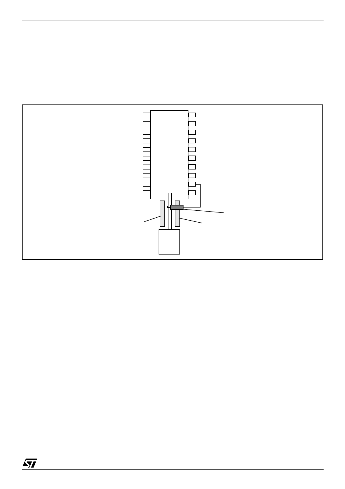
2.1 PCB LAYOUT RECOMMENDATION
In the case of DIP20 de vices the user s hould layout the PCB so that the DIP20 ST7261 device and
the USB connector are centered on the same axis
ensuring that the D- and D+ lines are of equal
len g th . Refe r to Figure 4
Figure 4. Recommended PCB Layout for USB Interface with DIP20 package
14
13
12
11
15
16
17
18
USBVCC
USBDP
1
2
3
4
5
6
7
8
9
10
19
20
USBDM
USB Connect o r
Ground
Ground
ST7261
1.5KOhm pull-up resistor
ST7261
8/80
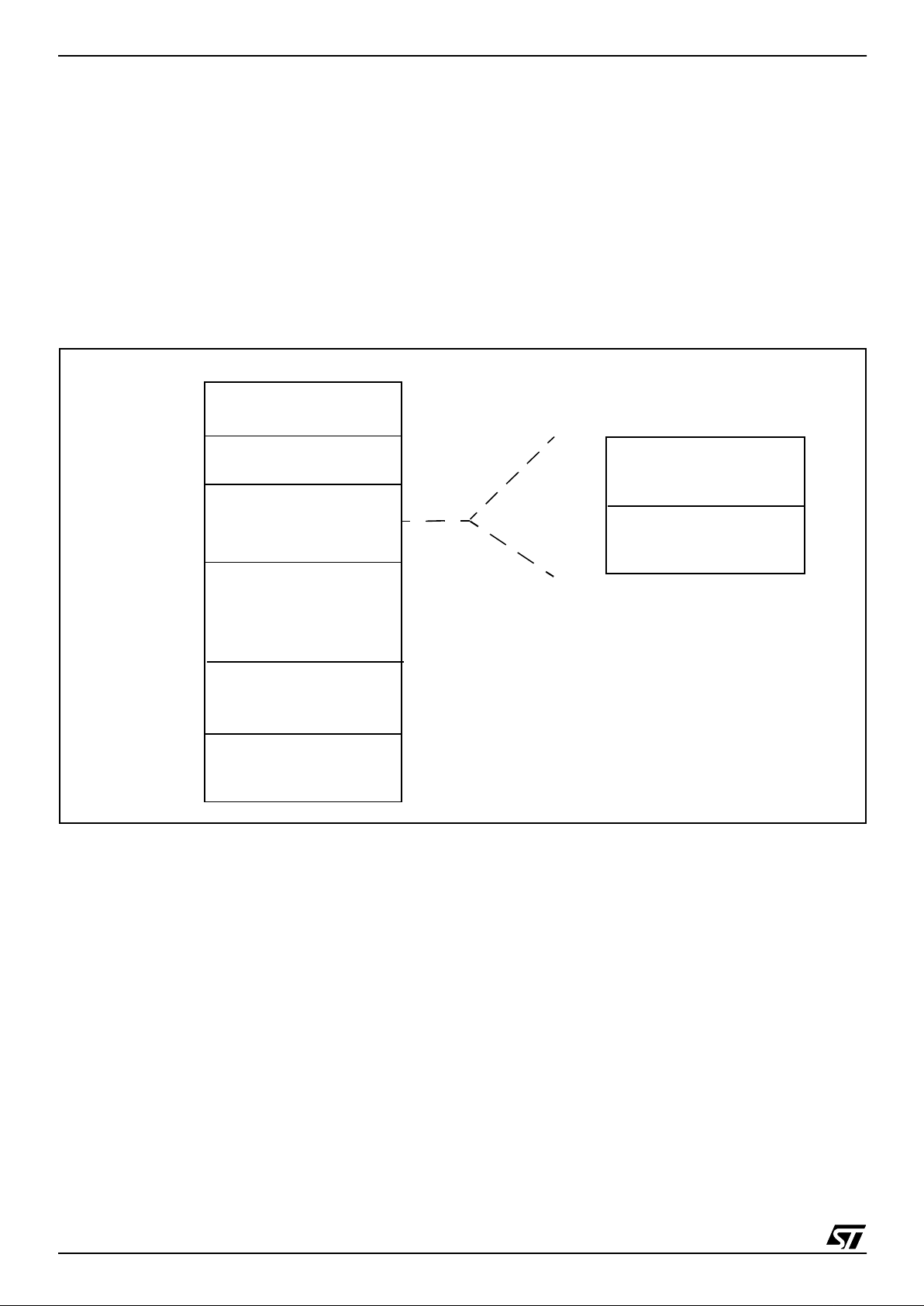
3 REGISTER & MEMORY MAP
As shown in the Figure 5, the MCU i s capable of
addressing 64K bytes of memories and I/O registers.
The available memory locations consist of 64
bytes of register locations, 256 bytes of RA M and
4 Kbytes of user program memory. The RAM
space includes up to 128 bytes for the sta ck from
0100h to 017Fh.
The highest address bytes contain the user re set
and interrupt vectors.
IMPORTANT: Memory locations marked as “Reserved” must ne ver be accessed. A ccessi ng a reseved area can have u npredict able effects on the
device.
Figure 5. Me m ory M a p
0000h
Program Memory
Interrupt & Reset Vectors
HW Registers
0040h
003Fh
(see Table 2)
FFDFh
FFE0h
FFFFh
See Table 5 on page 21
0180h
Reserved
017Fh
Short Addressing RAM
Zero page
017Fh
0080h
00FFh
(4 KBytes)
F000h
(128 Bytes)
256 Bytes RAM
Stack or
(128 Bytes)
EFFFh
16-bit Addressing RAM
Reserved
0080h
007Fh
ST7261
9/80
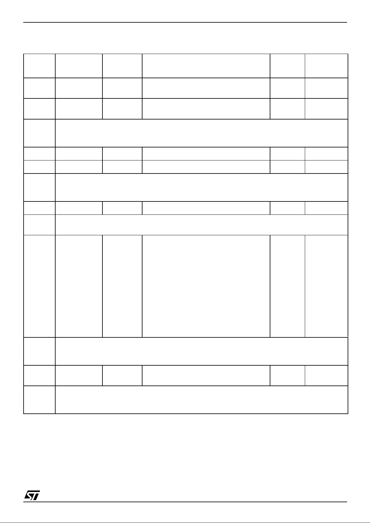
Table 2. Hardware Register M ap
Address Block
Register
Label
Register Name
Reset
Status
Remarks
0000h
0001h
Port A
PADR
PADDR
Port A Data Register
Port A Data Direction Register
00h
00h
R/W
R/W
0002h
0003h
Port B
PBDR
PBDDR
Port B Data Register
Port B Data Direction Register
00h
00h
R/W
R/W.
0004h
to
0007h
Reserved Area (4 Bytes)
0008h ITRFRE1 Interrupt Register 1 00h R/W
0009h MISC Miscellaneous Register 00h R/W
000Ah
to
000Ch
Reserved Area (2 Bytes)
000Dh WDG WDGCR Watchdog Control Register 7Fh R/W
000Eh to
0024h
Reserved Area (23 Bytes)
0025h
0026h
0027h
0028h
0029h
002Ah
002Bh
002Ch
002Dh
002Eh
002Fh
0030h
0031h
USB
USBPIDR
USBDMAR
USBIDR
USBISTR
USBIMR
USBCTLR
USBDADDR
USBEP0RA
USBEP0RB
USBEP1RA
USBEP1RB
USBEP2RA
USBEP2RB
USB PID Register
USB DMA Address register
USB Interrupt/DMA Register
USB Interrupt Status Register
USB Interrupt Mask Register
USB Control Register
USB Device Address Register
USB Endpoint 0 Register A
USB Endpoint 0 Register B
USB Endpoint 1 Register A
USB Endpoint 1 Register B
USB Endpoint 2 Register A
USB Endpoint 2 Register B
x0h
xxh
x0h
00h
00h
06h
00h
0000 xxxxb
80h
0000 xxxxb
0000 xxxxb
0000 xxxxb
0000 xxxxb
Read Only
R/W
R/W
R/W
R/W
R/W
R/W
R/W
R/W
R/W
R/W
R/W
R/W
0032h
to
0035h
Reserved Area (4 Bytes)
0036h
0037h
TBU
TBUCV
TBUCSR
TBU Counter Value Register
TBU Control/Status Register
00h
00h
R/W
R/W
0038h
to
003Fh
Reserved Area (8 Bytes)
ST7261
10/80
4 CENTRAL PROCE SSING UNIT
4.1 INTRODUCTION
This CPU has a full 8-bit architecture and contains
six internal registers allowing efficient 8-bit data
manipulation.
4.2 MAIN FEATURES
■ Enable executing 63 basic instructions
■ Fast 8-bit by 8-bit multiply
■ 17 main addressing modes (with indirect
addressing mode)
■ Two 8-bit index registers
■ 16-bit stack pointer
■ Low power HALT and WAIT modes
■ Priority maskable hardware interrupts
■ Non-maskable software/hardware interrupts
4.3 CPU REGISTERS
The 6 CPU registers shown in Figure 6 are not
present in the memory mapping and are accessed
by spec ifi c ins t ru c tio n s .
Accumulator (A)
The Accumulator is an 8-bit general purpose register used to hold operands and the res ults of the
arithmetic and logic calculations and to manipulate
data.
Index Registers (X and Y)
These 8-bit registers are used to create effective
addresses or as tempo rary storage areas f or data
manipulation. (The Cross -Assembler generates a
precede instruction (PRE) to indicate that the following instruction refers to the Y register.)
The Y register is not affected by the interrupt automatic procedures.
Program Counter (PC)
The program counter is a 16-bit register containing
the address of the next instruction to be executed
by the CPU. It is made of two 8-bit registers PCL
(Program Counter Low which is the LSB) and PCH
(Program Counter High which is the MSB).
Figure 6. CPU Registers
ACCUMULATOR
X INDEX REGISTER
Y INDEX REGISTER
STACK POINTER
CONDITION CODE REGISTER
PROGRAM COUNTER
70
1C1I1HI0NZ
RESET VALUE = RESET VECTOR @ FFFEh-FFFFh
70
70
70
0
7
15 8
PCH
PCL
15
8
70
RESET VALUE = STACK HIGHER ADDRESS
RESET VALUE =
1X11X1XX
RESET VALUE = XXh
RESET VALUE = XXh
RESET VALUE = XXh
X = Undefined Value
ST7261
11/80
CENTRAL PROC ESSING UNIT (Cont’d)
Condition Code Register (CC)
Read/Write
Reset Value: 111x1xxx
The 8-bit Condition Code regist er contains the i nterrupt masks and four flags representative of the
result of the instruction just executed. This register
can also be handled by the PUSH and POP instructions.
These bits can be individually tested and/or controlled by specific instructions.
Arithmetic Management Bits
Bit 4 = H
Half carry
.
This bit is set by hardware when a carry occurs between bits 3 and 4 of t he ALU during an ADD or
ADC instructions. It is reset by hardware during
the same instructio n s.
0: No half carry has occurred.
1: A half carry has occurred.
This bit is tested using the JRH or JRNH instruction. The H bit is useful in BCD arithmetic subroutine s .
Bit 2 = N
Negative
.
This bit is set and cleared by hardware. It is representative of the result sign of the last arithmetic,
logical or data manipulation. I t’s a copy of the result 7
th
bit.
0: The result of the last operation is positive or null.
1: The result of the last operation is negative
(i.e. the most significant bit is a logic 1).
This bit is accesse d by the JRMI and JRPL instructions.
Bit 1 = Z
Zero
.
This bit is set and cleared by hardware. This bit indicates that the result of the last arithmetic, logical
or data manipulation is zero.
0: The result of the last operation is different from
zero.
1: The result of the last operation is zero.
This bit is accessed by the JREQ and JRNE test
instructions.
Bit 0 = C
Carry/borrow.
This bit is set and cleared b y hardware and software. It indicates an overflow or an un derflow has
occurred during the last arithmetic operation.
0: No overflow or underflow has occurred.
1: An overflow or underflow has occurred.
This bit is driven by the SCF and RCF instructions
and tested by the JRC and JRNC instructions. It i s
also affected by the “bit test and branch”, shift and
rotate instructions.
Interrupt Managem e nt B i ts
Bit 5,3 = I1, I0
Interrupt
The combination of the I1 and I0 bits gives the current interrupt software priority.
These two bits are set/cleared by hardware when
entering in interrupt. The loaded value is given by
the corresponding bits in the interrupt software priority registers (IxSPR). They can be also set/
cleared by software with the RIM, SIM, IRET,
HALT, WFI and PUSH/POP instructions.
See the interrupt management chapter for more
details.
70
11I1HI0NZ
C
Interrupt Software Priorit y I1 I0
Level 0 (main) 1 0
Level 1 0 1
Level 2 0 0
Level 3 (= interrupt disable) 1 1
ST7261
12/80
CPU REGISTERS (Cont’d)
STACK POINTER (SP)
Read/Write
Reset Value: 017Fh
The Stack Pointer is a 16-bit register which is always pointing to the next free location in the stack.
It is then decremented after data has been pushed
onto the stack and incremented before data is
popped from the stack (see Figure 7).
Since the stack is 128 bytes deep, the 9 most significant bits are forced by hard ware. Following a n
MCU Reset, or after a Reset Stack Pointer instruction (RSP), the Stack Pointer contains its reset value (the SP6 to SP0 bits are set) which is the stack
higher address.
The least significant byte of the Stack Pointer
(called S) can be directly accessed by a LD instruction.
Note: When the lower limit is exceeded, the Stack
Pointer wraps around to the stack upper limit, without indicating the stack overflow. The previously
stored information is then o verwritten and therefore lost. The stack also wraps in case of an underflow.
The stack is used to sav e the return address during a subroutine call and the CPU context during
an interrupt. The user may also directly manipulate
the stack by means of the PUSH and POP instructions. In the case of an interrupt, the PCL is stored
at the first location po inted t o by t he SP. Th en t he
other registers are stored in the next locations as
shown in Figure 7.
– When an interrupt is received, the SP is decre-
mented and the context is pushed on the stack.
– On return from interrupt, the SP is incremented
and the context is popped from the stack.
A subroutine call occupies two locations and an interrupt five locat ion s i n the stack ar ea.
Figure 7. Stack Manipulation Example
15 8
00000001
70
1 SP6 SP5 SP4 SP3 SP2 SP1 SP0
PCH
PCL
SP
PCH
PCL
SP
PCL
PCH
X
A
CC
PCH
PCL
SP
PCL
PCH
X
A
CC
PCH
PCL
SP
PCL
PCH
X
A
CC
PCH
PCL
SP
SP
Y
CALL
Subroutine
Interrupt
Event
PUSH Y POP Y IRET
RET
or RSP
@ 017Fh
@ 0100h
Stack Higher Address = 017Fh
Stack Lower Address =
0100h
ST7261
13/80
5 CLOCKS AND RESET
5.1 CLOCK SYSTEM
5.1.1 General Description
The MCU accepts either a Crystal or Ceramic resonator, or an external clock signal to drive the internal oscillator. The internal clock (f
CPU
) is de-
rived from the external oscillator frequency (f
OSC
),
by dividing by 3 and multiplying by 2. By setting the
OSC12/6 bit in the option byte, a 12 MHz ex ternal
clock can be used giving an internal frequency of 8
MHz while maintaining a 6 MHz clock for USB (refer to Figure 10).
The internal clock signal (f
CPU
) consists of a
square wave with a duty cycle of 50%.
It is further divided by 1, 2, 4 or 8 depending on the
Slow Mode Selection bits in the Miscellaneous
register ( SMS[1:0 ])
The internal oscillat or is designed to operate with
an AT-cut parallel resonant quartz or ceramic resonator in the frequency range specified for f
osc
.
The circuit shown in Figure 9 is recommended
when using a crystal, and Table 3 lists the recommended capacitors. The crystal and associated
components shoul d be m ounted as close as possible to the input pins in order to minimize output
distortion and start-up stabilization time.
Table 3. Recommended Values for 12 MHz
Crystal Resonator
Note: R
SMAX
is the equivalent serial resistor of the
crystal (see crystal specification).
5.1.2 External Clock input
An external clock may be applied to the OSCIN input with the OSCOUT pin not connected, as
shown on F igure 8. The t
OXOV
specifications does
not apply when using an external clock input. The
equivalent specification of the external clock
source should be used instead of t
OXOV
(see Elec-
tr ical C haracteristic s).
5.1.3 Clock Output Pin (MCO)
The internal clock (f
CPU
) can be output on Port B0
by setting the MCO bit in the Misce llaneous register.
Figure 8. External Clock Source Connections
Figure 9. Crystal/Ceramic Resonator
Figure 10. Clock block diagram
R
SMAX
20
Ω
25
Ω
70
Ω
C
OSCIN
56pF 47pF 22pF
C
OSCOUT
56pF 47pF 22pF
R
P
1-10 M
Ω
1-10 M
Ω
1-10 M
Ω
OSCIN OSCOUT
EXTERNAL
CLOCK
NC
OSCIN
OSCOUT
C
OSCIN
C
OSCOUT
to CPU and
f
CPU
8/4/2/1 MHz
6 MHz (USB)
12 or
peripherals
%2
0
1
OSC12/6
6 MHz
Crystal
x2
Slow
Mode
%
SMS[1:0]
1/2/4/8
%3
(or 4/2/1/0.5 MHz)
MCO pin
ST7261
14/80
5.2 RESET
The Reset procedure is used to provide an orderly
software start-up or to exit low power modes.
Three reset modes are provided: a low voltage reset, a watchdog reset and an ext ernal reset at the
RESET
pin.
A reset causes the reset vector to be fetched from
addresses FFFEh and FFFFh in order to be loaded
into the PC and with program execution starting
from this point.
An internal circuitry provides a 5 14 CPU clock cycle delay from the time that the oscillator becomes
active.
5.2.1 Low Voltage Reset
Low voltage reset circuitry generates a reset when
V
DD
is:
■ below V
IT+
when VDD is rising,
■ below V
IT-
when VDD is falling.
During low voltage reset, the RESET
pin is held low,
thus permitting the MCU to reset other devices.
The Low Voltage Detector can be disabled by setting the LVD bit of the Option byte.
5.2.2 Watchdog Reset
When a watchdo g reset occ urs, t he RESET
pin is
pulled low permitting the MCU to reset other devices as when low voltage reset (Figur e 11).
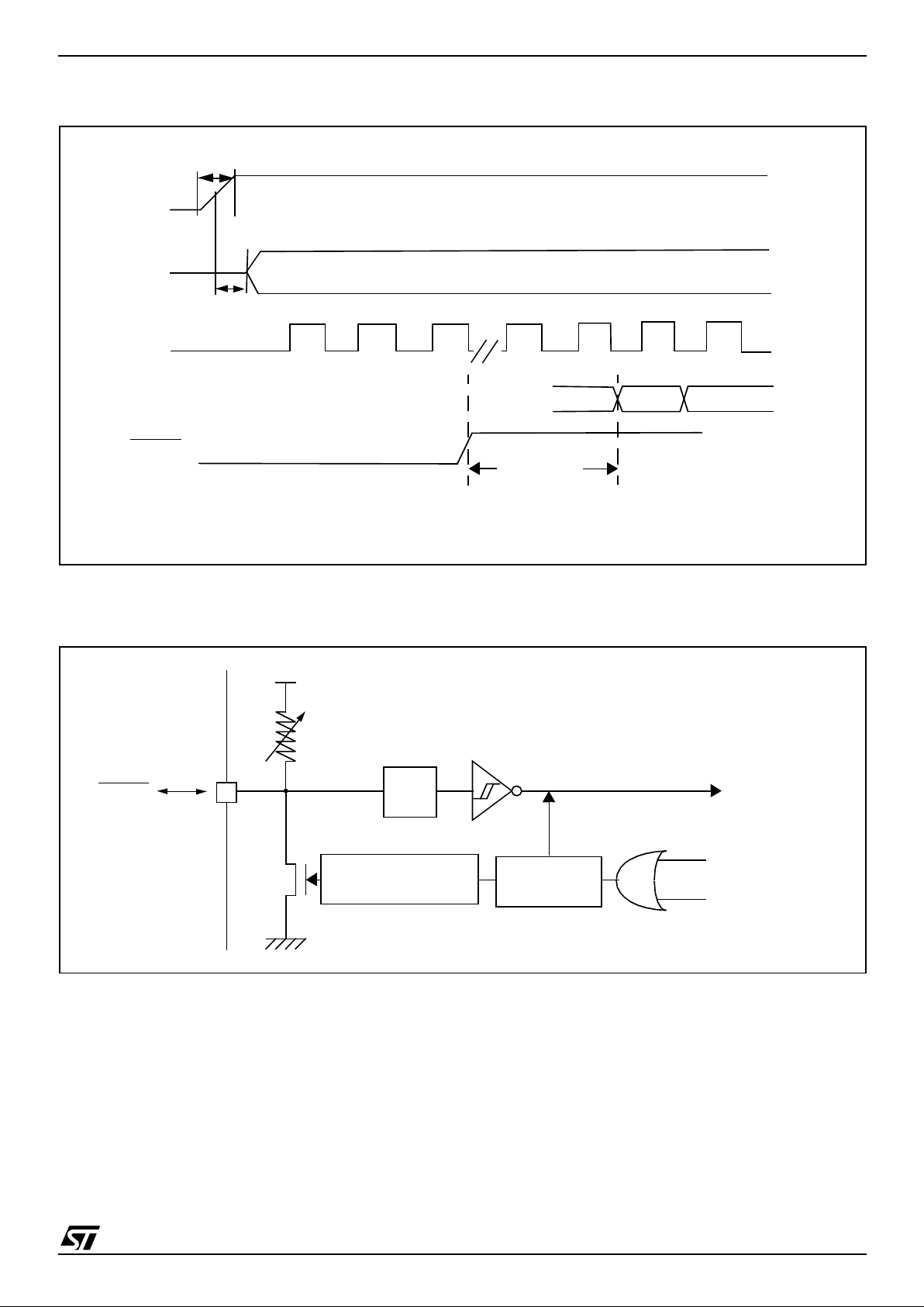
5.2.3 External Reset
The external reset is an active low input signal applied to the RESET
pin of the MCU.
As shown in Figure 14, the RESET
signal must
stay low for a minimum of one and a half CPU
clock cycles.
An internal Schmitt trigger at the RESET
pin is pro-
vided to improve noise immunity.
Figure 11. Low Voltage Reset functional Diagram
Figure 12. Low Voltage Reset Signal Output
Note: Typical hysteresis (V
IT+-VIT-
) of 250 mV is
expected
Figure 13. Temporization Timing Diagram after an internal Reset
LOW VOLTAGE
V
DD
FROM
WATCHDOG
RESET
RESET
INTERNAL
RESET
RESET
RESET
V
DD
V
IT+
V
IT-
V
DD
Addresses
$FFFE
Temporization
V
IT+
(514 CPU clock cycles)
ST7261
15/80
Figure 14. Reset Timing Diagra m
Note: Refer to Electrical Characteristics for values of t
DDR
, t
OXOV
, V
IT+
and V
IT-.
Figure 15. Reset Block Diagram
Note: The output of the external reset circuit must have an open-drain output to drive the ST7 reset pad.
Otherwise the device can be damaged when the ST7 generates an internal reset (LVD or watchdog).
V
DD
OSCIN
f
CPU
FFFF
FFFE
PC
RESET
t
DDR
t
OXOV
514 CPU
CLOCK
CYCLES
DELAY
RESET
R
ON
V
DD
WATCHDOG RESET
LVD RESET
INTERNAL
RESET
PULSE
GENERATOR
200ns
Filter
t
w(RSTL)out
+ 128 f
OSC
delay
ST7261
16/80
6 INTERRUP T S
6.1 INTRODUCTION
The CPU enhanced interrupt management provides the following features:
■ Hardware interrupts
■ Software interrupt (TRAP)
■ Nested or concurrent interrupt management
with flexible interrupt priority and level
management:
– Up to 4 software programmable nesting levels
– Up to 16 interrupt vectors fixed by hardware
– 3 non maskable events: RESET, TRAP, TLI
This interrupt management is based on:
– Bit 5 and bit 3 of the CPU CC register (I1:0),
– Interrupt software priority registers (ISPRx),
– F ixed interrupt vecto r addresses locat ed at the
high addresses of the memory map (FFE0h to
FFFFh) sorted by hardware priority order.
This enhanced interrupt cont roller guarantees full
upward compatibility with the standard (not nested) CPU interrupt controller.
6.2 MASKI N G AND PRO C ESSING FLOW
The interrupt masking is managed by the I1 and I0
bits of the CC register and the ISPRx registers
which give the interrupt software priority level of
each interrupt vector (see Table 4 ). The processing flow is shown in Fi gure 16.
When an interrupt request has to be serviced:
– Normal processing is suspended at the end of
the current instruction execution.
– The PC, X, A and CC registers are saved onto
the stack.
– I1 and I0 bits of CC register are set according to
the corresponding values in the ISPRx registers
of the serviced interrupt vector.
– The PC is then loaded with the interrupt vector of
the interrupt to service and the first instruction of
the interrupt service routine is fetched (refer to
“Interrupt Mapping” table for vector addresses).
The interrupt service routine should end with the
IRET instruction which c auses the contents of t he
saved registers to be recovered from the stack.
Note: As a consequence of the IRET instruction,
the I1 and I0 bits will be restored from the stack
and the program in the previous level will resume.
Table 4. Interrupt Software Priority Levels
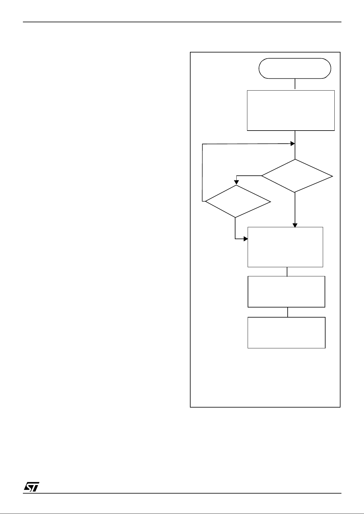
Figure 16. Int errupt Processing Flowchart
Interrupt software priority Level I1 I0
Level 0 (main) Low
High
10
Level 1 0 1
Level 2 0 0
Level 3 (= interrupt disable) 1 1
“IRET”
RESTORE PC, X, A, CC
STACK PC, X, A, CC
LOAD I1:0 FRO M INTER RUPT SW REG.
FETCH NEX T
RESET
TLI
PENDING
INSTRUCTION
I1:0
FROM STACK
LOAD PC FROM INTERRUPT VECTOR
Y
N
Y
N
Y
N
Interrupt has the same or a
lower software priority
THE INTERRUPT
STAYS PENDING
than c u rrent on e
Interrupt has a higher
softwarepriori ty
than current one
EXECUTE
INSTRUCTION
INTERRUPT
ST7261
17/80
INTERRUPTS (Cont’d)
Servicing Pending In te rrupts
As several interrupts can b e pen ding at the s ame
time, the interrupt to be taken into account is determined by the following two-step process:
– the highest software priority interrupt is serviced,
– i f several interrupts have the same software pri-
ority then the interrupt with the highest hardware
priority is serviced first.
Figure 17 describes this decision process.
Figure 17. Priority Decision Process
When an interrupt request is not serviced immediately, it is latched and then processed when its
software priority combined with the hardware priority becomes the highest one.
Note 1: The hardware priority is exclusive while
the software one i s not. This allows the prev ious
process to succeed with only one interrupt.
Note 2: RESET, TRAP and TLI can be considered
as having the highest softwa re priority in the d ecision process.
Different Interrupt Vector Sources
Two interrupt source types are managed by the
CPU interrupt controller: the non-maskable type
(RESET, TLI, TRAP) and the maskable type (external or from internal peripherals).
Non-Maskable Sources
These sources are processed regardless of the
state of the I1 and I0 bits of the CC register (see
Figure 16). After stacking the PC, X, A and CC
registers (except for RESET), the corresponding
vector is loaded in the PC register and t he I1 and
I0 bits of the CC are set to disable interrupts (level
3). These sources allow the processor to exit
HALT mode.
■ TLI (Top Level Hardware Interrupt)
This hardware interrupt occurs when a specific
edge is detected on the dedicated TLI pin.
Caution: A TRAP instruction must not be used in a
TLI serv i ce routine.
■ TRAP (Non Maskable Software Interrupt)
This software interrupt is serviced when the TRAP
instruction is executed. It will be serviced according to the flowchart in Figure 16 as a TLI.
Caution: TRAP can be interrupted by a TLI.
■ RESET
The RESET source has the highest priority in the
CPU. This means that the first current routine has
the highest software priority (level 3) and the highest hardware priority.
See the RESET chapter for more details.
Maskable Sources
Maskable interrup t vector sourc es can be servi ced
if the corresponding in terrupt is enabled and if its
own interrupt software priority (in ISPRx registers)
is higher than the one currently being serviced (I1
and I0 in CC register). If any of these two co nditions is false, the interrupt is la tched and thus remains pending.
■ External Interrupts
External interrupts allow the processor to exit from
HALT low power mode.
External interrupt sensitivity is software selectable
through the ITRFRE2 register.
External interrupt triggered on edge will be latched
and the interrupt request automatically cleared
upon entering the interrupt service routine.
If several input pins of a group connected to the
same interrupt line are selected simultaneously,
these w ill be log i cally NANDed.
■ Peripheral Interrupts
Usually the peripheral interrupts cause the Device
to exit from HALT mode except those mentioned in
the “Interrupt Mapping” table.
A peripheral interrupt occurs when a specific flag
is set in the peripheral status registers and if the
corresponding enable bit is set in the peripheral
control register.
The general sequence for clearing an interrupt is
based on an access to the status register followed
by a read or write to an associated register.
Note: The clearing sequence resets the internal
latch. A pending interrupt (i.e. waiting for being
serviced) will therefore be lost if the clear sequence is executed.
PENDING
SOFTWARE
Different
INTERRUPTS
Same
HIGHEST HARDWARE
PRIORITY SERVICED
PRIORITY
HIGHEST SOFTWARE
PRIORITY SERVICED
ST7261
18/80
INTERRUPTS (Cont’d)
6.3 INTERRUPTS AND LOW POWER MODES
All interrupts allow the processor to exit the WAIT
low power mode. On the contrary, only external
and other specified interrupt s allow the processor
to exit from the HALT modes (see column “Exit
from HALT” in “Interrupt Mapping” table). When
several pending interrupts are present whi le exiting HALT mode, the first one serviced can only be
an interrupt with e xit from HALT mode c apability
and it is selected through the same decision proc ess shown in Figure 17.
Note: If an interrupt, that is not able to Exit from
HALT mode, is pending with the highest priority
when exiting HALT mode, this interrupt is serviced
after the first one serviced.
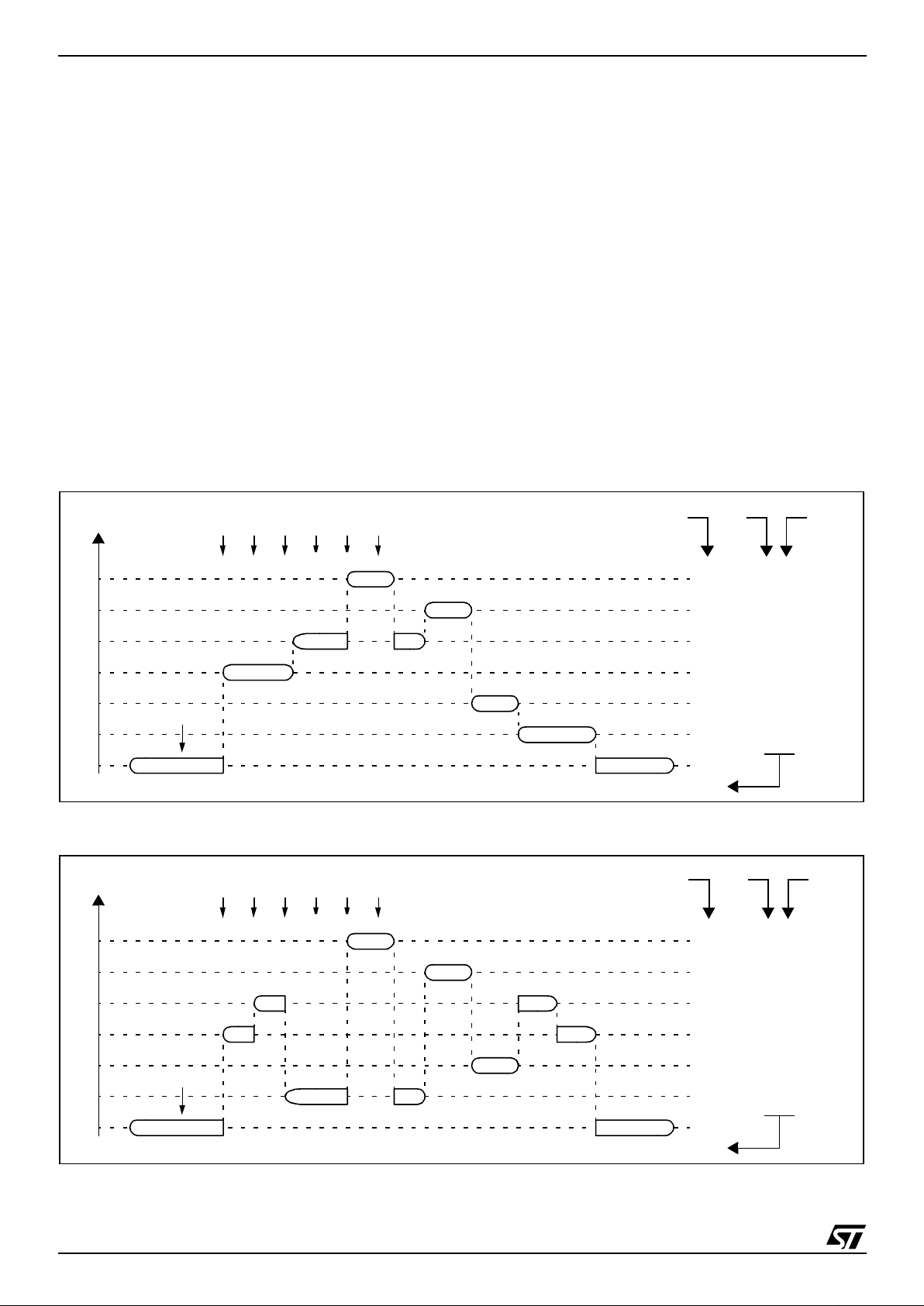
6.4 CONCURRENT & NESTED MANAGEMENT
The following Figure 18 and Figure 19 show two
different interrupt management modes. The first is
called concurrent mode and do es not allow an interrupt to be interrupted, unlike the nested mode in
Figure 19. The interrupt hardware priority is given
in this order from the l owes t to the hi ghest: M A IN,
IT4, IT3, IT2, IT1, IT0, TLI. The software priority is
given for each interrupt.
Warning: A stack overflow may occur without notifying the software of the failure.
Figure 18. Concurrent Interru pt Manage m ent
Figure 19. Nested Interrupt Management
MAIN
IT4
IT2
IT1
TLI
IT1
MAIN
IT0
I1
HARDWARE PRIORITY
SOFTWARE
3
3
3
3
3
3/0
3
11
11
11
11
11
11 / 10
11
RIM
IT2
IT1
IT4
TLI
IT3
IT0
IT3
I0
10
PRIORITY
LEVEL
USED STACK = 10 BYTES
MAIN
IT2
TLI
MAIN
IT0
IT2
IT1
IT4
TLI
IT3
IT0
HARDWARE PRIORITY
3
2
1
3
3
3/0
3
11
00
01
11
11
11
RIM
IT1
IT4
IT4
IT1
IT2
IT3
I1 I0
11 / 10
10
SOFTWARE
PRIORITY
LEVEL
USED STACK = 20 BYTES
ST7261
19/80
INTERRUPTS (Cont’d)
6.5 INTERRUPT REGISTER DESCRIPTION
CPU CC REGISTER INTERRUPT BITS
Read/Write
Reset Value: 111x 1010 (xAh)
Bit 5, 3 = I1, I0
Soft w a re In te r rupt Prio rity
These two bits indicate the current interrupt software priority.
These two bits are set/cle ared by hardware whe n
entering in interrupt. The loaded value is given by
the corresponding bits in the interrupt software priority registers (ISPRx).
They can be also s et/cleared by s oft ware wi th the
RIM, SIM, HALT, WFI, IRET and PUSH/POP instructions (see “Interrupt Dedicated Instruction
Set” table).
*Note: TLI, TRAP and RESET events ca n in terru pt
a level 3 program.
INTERRUPT SOFTWARE PRIORITY REGISTERS (ISPRX)
Read/Write (bit 7:4 of ISPR3 are read only)
Reset Value: 1111 1111 (FFh)
These four registers contain the interrupt software
priority of each interrupt vector.
– Each interrupt vector (except RESET and TRAP)
has corresponding bits in these registers where
its own software priority is stored. This correspondance is shown in the following table.
– Each I1_x and I0_x bit value in the ISPRx regis-
ters has the same meaning as the I1 and I0 bits
in the CC register.
– Level 0 can not be written (I1_x=1, I0_x=0). In
this case, the previously stored value is kept. (example: previous=CFh, write=64h, result=44h)
The RESET, TRAP a nd TLI vectors have no s oftware priorities. When one is serviced, the I1 and I0
bits of the CC register are both set.
*Note: Bits in the ISPRx registers which correspond to the TLI can be read and written but they
are not significant in the interrupt process management.
Caution: If the I1_x and I0_x bits are modified
while the interrupt x is execu ted the following behaviour has to be considered: If the interrupt x is
still pending (new interrupt or flag not cleared) and
the new software priority is highe r than the previous one, the interrupt x is re-ent ered. Otherwise,
the software priority stays unchanged up to the
next interrupt request (after the IRET of the interrupt x).
70
11I1 H I0 NZC
Interrupt Software Priority Level I1 I0
Level 0 (main)
Low
High
10
Level 1 0 1
Level 2 0 0
Level 3 (= interrupt disable*) 1 1
70
ISPR0 I1_3 I0_3 I1_2 I0_2 I1_1 I0_1 I1_0 I0_0
ISPR1 I1_7 I0_7 I1_6 I0_6 I1_5 I0_5 I1_4 I0_4
ISPR2 I1_11 I0_11 I1_10 I0_10 I1_9 I0_9 I1_8 I0_8
ISPR3 1 1 1 1 I1_13 I0_13 I1_12 I0_12
Vector address ISPRx bits
FFFBh-FFFAh I1_0 and I0_0 bits*
FFF9h-FFF8h I1_1 and I0_1 bits
... ...
FFE1h-FFE0h I1_13 and I0_13 bits
ST7261
20/80
6.6 Interrupt Register
INTERRUPT REGISTER 1 (ITRFRE1)
Address: 0008h - Read/Write
Reset Value: 0000 0000 (00h)
Bit 7:0 = ITiE
Interrupt Enable
0: I/O pin free for general purpose I/O
1: ITi external interrupt enabled.
Note: The corresponding interrupt is generated
when:
– a rising edge occurs on the IT5/IT6 pins
– a falling edge occurs on the IT1, 2, 3, 4, 7 and 8
pins
INTERRUPT REGISTER 2 (ITRFRE2)
Address: 0039h - Read/Write
Reset Value: 0000 0000 (00h)
Bit 7:6 = CTL[3:2]
IT[12:11] Interrupt Sensitivity
These bits are set and cleared by software. They
are used to configure the edge and level sensitivity
of the IT12 and IT11 external interrupt pins (this
means that both must have the same sensitivity).
Bit 5:4 = CTL[1:0]
IT[10:9]1nterrupt Sensitivity
These bits are set and cleared by software. They
are used to configure the edge and level sensitivity
of the IT10 and IT9 external interrupt pins (this
means that both must have the same sensitivity).
Bit 3:0 = ITiE
Interrupt Enable
0: I/O pin free for general purpose I/O
1: ITi external interrupt enabled.
70
IT8E IT7E IT 6E IT5E IT4E IT3E IT2E IT1E
70
CTL3 CTL2 CTL1 CTL0 IT12E IT11E IT10E IT9E
CTL3 CTL2 IT[12:11] Sensitivity
0 0 Falling edge and low level
0 1 Rising edge only
1 0 Falling edge only
1 1 Rising and falling edge
CTL1 CTL0 IT[10:9] Sensitivity
0 0 Falling edge and low level
0 1 Rising edge only
1 0 Falling edge only
1 1 Rising and falling edge
ST7261
21/80
INTERRUPTS (Cont’d)
Table 5. I nte rrupt Mapping
Table 6. Nested Interrupts Register Map and Reset Values
N°
Source
Block
Description
Register
Label
Exit
from
HALT
Address
Vector
Priority
Order
Reset Vector Yes FFFEh-FFFFh
Highest
Priority
Lowest
Priority
TRAP software interrupt vector No FFFCh-FFFDh
0 NOT USED FFFAh-FFFBh
1 USB USB End Suspend interrupt vector USBISTR Yes FFF8h-FFF9h
2
I/O Ports
Port A external interrupts IT[3:1]
ITRFRE1
Yes FFF6h-FFF7h
3 Port B external interrupts IT[8:5] Yes FFF4h-FFF5h
4 NOT USED FFF2h-FFF3h
5 TBU Timebase Unit interrupt vector TBUCSR No FFF0h-FFF1h
6 NOT USED FFEEh-FFEFh
7 NOT USED FFECh-FFEDh
8 NOT USED FFEAh-FFEBh
9 USB USB interrupt vector USBISTR No FFE8h-FFE9h
10 NOT USED FFE6h-FFE7h
Address
(Hex.)
Register
Label
76543210
0032h
ISPR0
Reset Value
Ext. Interrupt Port B Ext. Interrupt Port A USB END SUSP Not Used
I1_3
1
I0_3
1
I1_2
1
I0_2
1
I1_1
1
I0_1
111
0033h
ISPR1
Reset Value
SPI ART TBU Ext. Interrupt Port C
I1_7
1
I0_7
1
I1_6
1
I0_6
1
I1_5
1
I0_5
1
I1_4
1
I0_4
1
0034h
ISPR2
Reset Value
Not Used ADC USB SCI
I1_11
1
I0_11
1
I1_10
1
I0_10
1
I1_9
1
I0_9
1
I1_8
1
I0_8
1
0035h
ISPR3
Reset Value1111
Not Used Not Used
I1_13
1
I0_13
1
I1_12
1
I0_12
1
ST7261
22/80
7 POWER SAVING MODES
7.1 INTRODUCTION
There are three Power Saving modes. Slow Mode
is selected by setting the SMS bits in the Miscellaneous register. Wait and Halt modes may be entered using the WFI and HALT instructions.
After a RESET the normal operating mode is selected by default (RUN mode). This mode drives
the device (CPU and embedded peripherals) by
means of a master clock which is based on the
main oscillator f requency divide d by 3 and multiplied by 2 (f
CPU
).
From Run mode, the different power saving
modes may be selected by setting the relevant
register bits or by calling the specific ST7 software
instruction whose action depends on the oscillator
status.
7.1.1 Slow Mode
In Slow mode, the osc illator frequency can be d ivided by a value defined in the Miscellaneous
Register. The CPU and peripherals are clocked at
this lower frequency. Slow mode is used to reduce
power consumption, and enables the user to adapt
clock frequency to available supply voltage.
7.2 WAIT MODE
WAIT mode places the MCU in a low power c onsumption mode by stopping the CPU.
This pow e r s a v ing mo de is se lected b y ca llin g the
“WFI” ST7 software instruction.
All peripherals remain active. During WAIT mode,
the I bit of the CC register is forced to 0, to enable
all interrupts. All other registers and memory remain unchanged. The MCU remains in WAIT
mode until an interrupt or Res et oc curs, where upon the Program Counter branches to the starting
address of the interrupt or Reset service routine.
The MCU w ill re mai n in W AIT mo de unt il a Res et
or an Interrupt occurs, causing it to wake up.
Refer to Figure 20.
Figure 20. WAIT Mode Flow Chart
WFI INSTRUCTION
RESET
INTERRUPT
Y
N
N
Y
CPU CLOCK
OSCILLATOR
PERIPH. CLOCK
I-BIT
ON
ON
CLEARED
OFF
CPU CLOCK
OSCILLATOR
PERIPH. CLOCK
I-BIT
ON
ON
SET
ON
FETCH RESET VECTOR
OR SERVICE INTERRUPT
514 CPU CLOCK
CYCLES DELAY
IF RESET
Note: Before servicing an interrupt, the CC register is
pushed on the sta ck. The I-Bit is s et d uring the inte rrupt routine and cleared when the CC register is
popped.
ST7261
23/80
POWER SAVING MODES (Cont’d)
7.3 HALT MODE
The HALT mode is the MCU lowest power consumption mode. The HALT mode is entered by executing the HALT instruction. The internal oscillator is then turned off, causing all internal processing to be stopped, including the operation of the
on-chip peripherals.
When entering HALT mode, the I bit in the Condition Code Register is cleared. Thus, any of the external interrupts (ITi or US B end suspend mode),
are allowed and if an interrupt occurs, the CPU
clock becomes active.
The MCU can e xit HAL T mode on reception of either an external interrupt on ITi, an end suspen d
mode interrupt coming from USB peripheral, or a
reset. The osc illato r is t hen t ur ned on and a stabilization time is provided before rele as ing CPU operation. The stabilization time is 514 CPU clock cycles.
After the start up delay, the CPU continues operation by servicing the interrupt which wakes it up or
by fetching the reset vector if a reset wakes it up.
Figure 21. HALT Mod e Flo w C ha r t
N
N
EXTERNAL
INTERRUPT*
RESET
HALT INSTRUCTION
514 CPU CLOCK
FETCH RESET VECTOR
OR SERVICE INTERRUPT
CYCLES DELAY
CPU CLOCK
OSCILLATOR
PERIPH. CLOCK
I-BIT
ON
ON
SET
ON
CPU CLOCK
OSCILLATOR
PERIPH. CLOCK
I-BIT
OFF
OFF
CLEARED
OFF
Y
Y
Note: Before servicing an interrupt, the CC register is
pushed on the stac k. T he I -Bit i s se t du ring the interrupt routine and cleared when the CC register is
popped.
ST7261
24/80
8 I/O PORTS
8.1 INTRODUCTION
The I/O ports offer different functional modes:
transfer of data through digital inputs and outputs
and for specific pins:
– Analog signal input (ADC)
– Alternate signal input/out put for the on-chip pe-
ripherals.
– External interrupt generation
An I/O port i s c om posed of up to 8 pins. Each pi n
can be programmed independently as digital input
or digital output.
8.2 FUNCTIONAL DESCRIPTION
Each port is associated with 2 main registers:
– Data Register (DR)
– Data Direction Register (DDR)
Each I/O pin may be programmed using the corre-
sponding register bits in DDR regi ster: bi t x corresponding to pin x of the port. The same correspondence is used for the DR register.
Table 7. I /O Pi n Fu nc ti ons
8.2.1 Input Modes
The input configuration is s ele cted by clearing the
corresponding DDR register bit.
In this case, reading the DR register returns the
digital value applied to the external I/O pin.
Notes:
1. All the inputs are triggered by a Schmitt trigger.
2. When switching from input mode to output
mode, the DR reg ister should be writte n first to
output the correct value as s oon as the port is
configured as an output.
Interrupt function
When an external interrupt function of an I/O pin, is
enabled using the ITFRE registers, an event on
this I/O can generate an external Interrupt request
to the CPU. The i nterrupt sensitivit y is programma-
ble, the options are given in the description of the
ITRFRE interrupt registers.
Each pin can independently generate an I nterrupt
request.
Each external interrupt vecto r is linked to a dedicated group of I/O port pins (see Interrupts section). If more than one input pin is selected sim ultaneously as interrupt source, this is logically ANDed and inverted. For this reason, if an event occurs on one of the i nterrupt pins, it masks t he other
ones.
8.2.2 Output Mode
The pin is configured in output mode by setting the
corresponding DDR register bit (see Table 7).
In this mode, writing “0” or “1” to the DR register
applies this digital value to the I/O pin through the
latch. Then reading the DR register returns the
previously stored value.
Note: In this mode, the interrupt function is disabled.
8.2.3 Alternate Functions
Digital A lternate Fu nct i on s
When an on-chip peripheral is configured to use a
pin, the alternate function is au tomatically selected. This alternate function takes priority over
standard I/O programming. When the signal is
coming from an on-chip peripheral, the I/O pin is
automatically configured in output mode (push-pull
or open drain according to the peripheral).
When the signal is goi ng t o an on-c hip pe ripheral,
the I/O pin ha s to be configured in input m ode. In
this case, the pin state is also digitally readable by
addressing the DR register.
Notes:
1. Input pull-up conf iguration can cause a n unexpected value at the alternate peripheral input.
2. When the on-chip peripheral uses a pin as input
and output, this pin must be configured as an
input (DDR = 0).
Warning
: Alternate functions of peripherals must
must not be activated when the external interrupts
are enabled on the same pin, in order to avoid
generating spurious interrupts.
DDR MODE
0 Input
1 Output
 Loading...