

SGS Thomson Microelectronics ST72F521R9, ST72F521R7, ST72F521R6, ST72F521M9, ST72F521M7 Datasheet
...
Rev. 1.9
August 2003 1/211
ST72521
8-BIT MCU WITH NESTED INTERRUPT S, FLASH, 10-BIT ADC,
FIVE TIMERS, SPI, SCI, I
2
C, CAN INTERFACE
■ Memories
– 32K to 60K dual voltage High De nsity Flash
(HDFlash) or ROM with read-out protection
capability. In-Application Programming and
In-Circuit Programming for HDFlash devices
– 1K to 2K RAM
– HDFlash endurance: 100 cycles, data reten-
tion: 20 years at 55°C
■ Clock , Res et And Supply Manag e me n t
– Enhanced low voltage supervisor (LVD) for
main supply and auxiliary voltage detector
(AVD) with interrupt capability
– Clock sources: crystal/ceramic res onator os-
cillators , inter nal RC oscillato r, clock se curity
system and bypass for external clock
– PLL for 2x frequency multiplication
– Four power saving modes: Halt, Active-Ha lt,
Wait and Slow
■ Interrupt Management
– Nested interrupt controller
– 14 interrupt vectors plus TRAP and RESET
– Top Level Interrupt (TLI) pin
– 15 external interrupt lines (on 4 vectors)
■ Up to 64 I/O Ports
– 48 multifunctional bidirectional I/O lines
– 34 alternate function lines
– 16 high sink outputs
■ 5 Timers
– Main Clock Controller with: Real time base,
Beep and Clock-out capab ilities
– Configurable watchdog timer
– Two 16-bit timers with: 2 input captures, 2 out-
put compares, external clock input on one tim-
er, PWM and pulse generator modes
– 8-bit PWM Auto-Reload timer with: 2 input
captures, 4 PWM outputs, output compare
and time base interrupt, external clock with
event detector
■ 4 Communications Interfaces
– SPI synchronous serial interface
– SCI asynchronous serial interface (LIN com-
patible)
–I
2
C multimaster interface
– CAN interface (2.0B Passive)
■ Analog peripheral
– 10-bit ADC with 16 input pins
■ Instruction Set
– 8-bit Data Manipulation
– 63 Basic Instructions
– 17 main Addressing Modes
– 8 x 8 Unsigned Multiply Instruction
■ Development Tools
– Full hardware/software development package
– In-Circuit Testing capability
Device Summary
TQFP80
14 x 14
TQFP64
10 x 10
TQFP64
14 x 14
Features ST72521(M/R/AR)9 ST72521(R/AR)6
Program memory - bytes 60K 32K
RAM (stack) - byte s 2048 (256) 1024 (256)
Operating Voltage 3.8V to 5.5V
Temp. Range up to -40°C to +125 °C
Package
TQFP8 0 14x14 (M), TQFP64 14x14 (R), TQFP64
10x10 (A R)
TQFP6 4 14x14 (R) , TQFP64 10x10 (AR)
1

Table of Cont ents
211
2/211
1 INTRODUCTION . . . . . . . . . . . . . . . . . . . . . . . . . . . . . . . . . . . . . . . . . . . . . . . . . . . . . . . . . . . . . 7
2 PIN DESCRIPTION . . . . . . . . . . . . . . . . . . . . . . . . . . . . . . . . . . . . . . . . . . . . . . . . . . . . . . . . . . . . 8
3 REGISTER & MEMORY MAP . . . . . . . . . . . . . . . . . . . . . . . . . . . . . . . . . . . . . . . . . . . . . . . . . . . 14
4 FLASH PROGRAM MEMORY . . . . . . . . . . . . . . . . . . . . . . . . . . . . . . . . . . . . . . . . . . . . . . . . . . 18
4.1 INTRODUCTION . . . . . . . . . . . . . . . . . . . . . . . . . . . . . . . . . . . . . . . . . . . . . . . . . . . . . . . 18
4.2 MAIN FEATURES . . . . . . . . . . . . . . . . . . . . . . . . . . . . . . . . . . . . . . . . . . . . . . . . . . . . . . 18
4.3 STRUCTURE . . . . . . . . . . . . . . . . . . . . . . . . . . . . . . . . . . . . . . . . . . . . . . . . . . . . . . . . . . 18
4.3.1 Read-out Protection . . . . . . . . . . . . . . . . . . . . . . . . . . . . . . . . . . . . . . . . . . . . . . . . 18
4.4 ICC INTERFACE . . . . . . . . . . . . . . . . . . . . . . . . . . . . . . . . . . . . . . . . . . . . . . . . . . . . . . . 19
4.5 ICP (IN-CIRCUIT PROGRAMMING) . . . . . . . . . . . . . . . . . . . . . . . . . . . . . . . . . . . . . . . . 20
4.6 IAP (IN-APPLICATION PROGRAMMING) . . . . . . . . . . . . . . . . . . . . . . . . . . . . . . . . . . . 20
4.7 RELATED DOCUMENTATION . . . . . . . . . . . . . . . . . . . . . . . . . . . . . . . . . . . . . . . . . . . . 20
4.7.1 Register Description . . . . . . . . . . . . . . . . . . . . . . . . . . . . . . . . . . . . . . . . . . . . . . . . 20
5 CENTRAL PROCESSING UNIT . . . . . . . . . . . . . . . . . . . . . . . . . . . . . . . . . . . . . . . . . . . . . . . . . 21
5.1 INTRODUCTION . . . . . . . . . . . . . . . . . . . . . . . . . . . . . . . . . . . . . . . . . . . . . . . . . . . . . . . 21
5.2 MAIN FEATURES . . . . . . . . . . . . . . . . . . . . . . . . . . . . . . . . . . . . . . . . . . . . . . . . . . . . . . 21
5.3 CPU REGISTERS . . . . . . . . . . . . . . . . . . . . . . . . . . . . . . . . . . . . . . . . . . . . . . . . . . . . . . 21
6 SUPPLY, RESET AND CLOCK MANAGEMENT . . . . . . . . . . . . . . . . . . . . . . . . . . . . . . . . . . . . 24
6.1 PHASE LOCKED LOOP . . . . . . . . . . . . . . . . . . . . . . . . . . . . . . . . . . . . . . . . . . . . . . . . . 24
6.2 MULTI-OSCILLATOR (MO) . . . . . . . . . . . . . . . . . . . . . . . . . . . . . . . . . . . . . . . . . . . . . . . 25
6.3 RESET SEQUENCE MANAGER (RSM) . . . . . . . . . . . . . . . . . . . . . . . . . . . . . . . . . . . . . 26
6.3.1 Introduction . . . . . . . . . . . . . . . . . . . . . . . . . . . . . . . . . . . . . . . . . . . . . . . . . . . . . . . 26
6.3.2 As ynchronous External RES ET pin . . . . . . . . . . . . . . . . . . . . . . . . . . . . . . . . . . . . 26
6.3.3 External Power-On RESET . . . . . . . . . . . . . . . . . . . . . . . . . . . . . . . . . . . . . . . . . . 27
6.3.4 Internal Low Voltage Detector (LVD) RESET . . . . . . . . . . . . . . . . . . . . . . . . . . . . . 27
6.3.5 Inte rnal Watchdog RE SET . . . . . . . . . . . . . . . . . . . . . . . . . . . . . . . . . . . . . . . . . . . 27
6.4 SYSTEM INTEGRITY MANAGEMENT (SI) . . . . . . . . . . . . . . . . . . . . . . . . . . . . . . . . . . 28
6.4.1 Low Voltage Detector (LVD) . . . . . . . . . . . . . . . . . . . . . . . . . . . . . . . . . . . . . . . . . . 28
6.4.2 Aux iliary Voltage Detector (AVD) . . . . . . . . . . . . . . . . . . . . . . . . . . . . . . . . . . . . . . 29
6.4.3 Clock Security System (CSS) . . . . . . . . . . . . . . . . . . . . . . . . . . . . . . . . . . . . . . . . . 31
6.4.4 Low Power Modes . . . . . . . . . . . . . . . . . . . . . . . . . . . . . . . . . . . . . . . . . . . . . . . . . 31
6.4.5 Register Description . . . . . . . . . . . . . . . . . . . . . . . . . . . . . . . . . . . . . . . . . . . . . . . . 32
7 INTERRUPTS . . . . . . . . . . . . . . . . . . . . . . . . . . . . . . . . . . . . . . . . . . . . . . . . . . . . . . . . . . . . . . . 33
7.1 INTRODUCTION . . . . . . . . . . . . . . . . . . . . . . . . . . . . . . . . . . . . . . . . . . . . . . . . . . . . . . . 33
7.2 MASKING AND PROCESSING FLOW . . . . . . . . . . . . . . . . . . . . . . . . . . . . . . . . . . . . . . 33
7.3 INTERRUPTS AND LOW POWER MODES . . . . . . . . . . . . . . . . . . . . . . . . . . . . . . . . . . 35
7.4 CONCURRENT & NESTED MANAGEMENT . . . . . . . . . . . . . . . . . . . . . . . . . . . . . . . . . 35
7.5 INTERRUPT REGISTER DESCRIPTION . . . . . . . . . . . . . . . . . . . . . . . . . . . . . . . . . . . . 36
7.6 EXTERNAL INTERRUPTS . . . . . . . . . . . . . . . . . . . . . . . . . . . . . . . . . . . . . . . . . . . . . . . 38
7.6.1 I/O Port Interrupt Sensitivity . . . . . . . . . . . . . . . . . . . . . . . . . . . . . . . . . . . . . . . . . . 38
7.7 EXTERNAL INTERRUPT CONTROL REGISTER (EICR) . . . . . . . . . . . . . . . . . . . . . . . 40
8 POWER SAVING MODES . . . . . . . . . . . . . . . . . . . . . . . . . . . . . . . . . . . . . . . . . . . . . . . . . . . . . 42
8.1 INTRODUCTION . . . . . . . . . . . . . . . . . . . . . . . . . . . . . . . . . . . . . . . . . . . . . . . . . . . . . . . 42
8.2 SLOW MODE . . . . . . . . . . . . . . . . . . . . . . . . . . . . . . . . . . . . . . . . . . . . . . . . . . . . . . . . . 42
2

Table of Cont ents
3/211
8.3 WAIT MODE . . . . . . . . . . . . . . . . . . . . . . . . . . . . . . . . . . . . . . . . . . . . . . . . . . . . . . . . . . 4 3
8.4 ACTIVE-HALT AND HALT MODES . . . . . . . . . . . . . . . . . . . . . . . . . . . . . . . . . . . . . . . . 44
8.4.1 ACTIVE-HALT MODE . . . . . . . . . . . . . . . . . . . . . . . . . . . . . . . . . . . . . . . . . . . . . . . 44
8.4.2 HALT MODE . . . . . . . . . . . . . . . . . . . . . . . . . . . . . . . . . . . . . . . . . . . . . . . . . . . . . . 45
9 I/O PORTS . . . . . . . . . . . . . . . . . . . . . . . . . . . . . . . . . . . . . . . . . . . . . . . . . . . . . . . . . . . . . . . . . . 4 7
9.1 INTRODUCTION . . . . . . . . . . . . . . . . . . . . . . . . . . . . . . . . . . . . . . . . . . . . . . . . . . . . . . . 47
9.2 FUNCTIONAL DESCRIPTION . . . . . . . . . . . . . . . . . . . . . . . . . . . . . . . . . . . . . . . . . . . . 47
9.2.1 I nput Mode s . . . . . . . . . . . . . . . . . . . . . . . . . . . . . . . . . . . . . . . . . . . . . . . . . . . . . . 47
9.2.2 Output Modes . . . . . . . . . . . . . . . . . . . . . . . . . . . . . . . . . . . . . . . . . . . . . . . . . . . . . 47
9.2.3 Alternate Functions . . . . . . . . . . . . . . . . . . . . . . . . . . . . . . . . . . . . . . . . . . . . . . . . . 47
9.3 I/O PORT IMPLEMENTATION . . . . . . . . . . . . . . . . . . . . . . . . . . . . . . . . . . . . . . . . . . . . 50
9.4 LOW POWER MODES . . . . . . . . . . . . . . . . . . . . . . . . . . . . . . . . . . . . . . . . . . . . . . . . . . 50
9.5 INTERRUPTS . . . . . . . . . . . . . . . . . . . . . . . . . . . . . . . . . . . . . . . . . . . . . . . . . . . . . . . . . 50
9.5.1 I/O Port Implementation . . . . . . . . . . . . . . . . . . . . . . . . . . . . . . . . . . . . . . . . . . . . . 51
10 ON-CHIP PERIPHERALS . . . . . . . . . . . . . . . . . . . . . . . . . . . . . . . . . . . . . . . . . . . . . . . . . . . . . 53
10.1 WATCHDOG TIMER (WDG) . . . . . . . . . . . . . . . . . . . . . . . . . . . . . . . . . . . . . . . . . . . . . . 53
10.1.1 Introduction . . . . . . . . . . . . . . . . . . . . . . . . . . . . . . . . . . . . . . . . . . . . . . . . . . . . . . . 53
10.1.2 Main Features . . . . . . . . . . . . . . . . . . . . . . . . . . . . . . . . . . . . . . . . . . . . . . . . . . . . . 53
10.1.3 Functional Description . . . . . . . . . . . . . . . . . . . . . . . . . . . . . . . . . . . . . . . . . . . . . . 53
10.1.4 How to Program the Watchdog Timeout . . . . . . . . . . . . . . . . . . . . . . . . . . . . . . . . . 54
10.1.5 Low Power Modes . . . . . . . . . . . . . . . . . . . . . . . . . . . . . . . . . . . . . . . . . . . . . . . . . 56
10.1.6 Hardware Watchdog Option . . . . . . . . . . . . . . . . . . . . . . . . . . . . . . . . . . . . . . . . . . 56
10.1.7 Using Halt Mode with the WDG (WDGHALT option) . . . . . . . . . . . . . . . . . . . . . . . 56
10.1.8 Interrupts . . . . . . . . . . . . . . . . . . . . . . . . . . . . . . . . . . . . . . . . . . . . . . . . . . . . . . . . . 56
10.1.9 Register Description . . . . . . . . . . . . . . . . . . . . . . . . . . . . . . . . . . . . . . . . . . . . . . . . 56
10.2 MAIN CLOCK CONTROLLER WITH REAL TIME CLOCK AND BEEPER (MCC/RTC) . 58
10.2.1 Programmable CPU Clock Prescaler . . . . . . . . . . . . . . . . . . . . . . . . . . . . . . . . . . . 58
10.2.2 Clock-out Capability . . . . . . . . . . . . . . . . . . . . . . . . . . . . . . . . . . . . . . . . . . . . . . . . 58
10.2.3 Real Time Clock Timer (RTC) . . . . . . . . . . . . . . . . . . . . . . . . . . . . . . . . . . . . . . . . 58
10.2.4 Beeper . . . . . . . . . . . . . . . . . . . . . . . . . . . . . . . . . . . . . . . . . . . . . . . . . . . . . . . . . . 58
10.2.5 Low Power Modes . . . . . . . . . . . . . . . . . . . . . . . . . . . . . . . . . . . . . . . . . . . . . . . . . 59
10.2.6 Interrupts . . . . . . . . . . . . . . . . . . . . . . . . . . . . . . . . . . . . . . . . . . . . . . . . . . . . . . . . . 59
10.2.7 Register Description . . . . . . . . . . . . . . . . . . . . . . . . . . . . . . . . . . . . . . . . . . . . . . . . 59
10.3 PWM AUTO-RELOAD TIMER (ART) . . . . . . . . . . . . . . . . . . . . . . . . . . . . . . . . . . . . . . . 61
10.3.1 Introduction . . . . . . . . . . . . . . . . . . . . . . . . . . . . . . . . . . . . . . . . . . . . . . . . . . . . . . . 61
10.3.2 Functional Description . . . . . . . . . . . . . . . . . . . . . . . . . . . . . . . . . . . . . . . . . . . . . . 62
10.3.3 Register Description . . . . . . . . . . . . . . . . . . . . . . . . . . . . . . . . . . . . . . . . . . . . . . . . 66
10.4 16-BIT TIMER . . . . . . . . . . . . . . . . . . . . . . . . . . . . . . . . . . . . . . . . . . . . . . . . . . . . . . . . . 70
10.4.1 Introduction . . . . . . . . . . . . . . . . . . . . . . . . . . . . . . . . . . . . . . . . . . . . . . . . . . . . . . . 70
10.4.2 Main Features . . . . . . . . . . . . . . . . . . . . . . . . . . . . . . . . . . . . . . . . . . . . . . . . . . . . . 70
10.4.3 Functional Description . . . . . . . . . . . . . . . . . . . . . . . . . . . . . . . . . . . . . . . . . . . . . . 70
10.4.4 Low Power Modes . . . . . . . . . . . . . . . . . . . . . . . . . . . . . . . . . . . . . . . . . . . . . . . . . 82
10.4.5 Interrupts . . . . . . . . . . . . . . . . . . . . . . . . . . . . . . . . . . . . . . . . . . . . . . . . . . . . . . . . 82
10.4.6 Summary of Timer modes . . . . . . . . . . . . . . . . . . . . . . . . . . . . . . . . . . . . . . . . . . . 82
10.4.7 Register Description . . . . . . . . . . . . . . . . . . . . . . . . . . . . . . . . . . . . . . . . . . . . . . . . 83
10.5 SERIAL PERIPHERAL INTERFACE (SPI) . . . . . . . . . . . . . . . . . . . . . . . . . . . . . . . . . . . 89
1

Table of Cont ents
211
4/211
10.5.1 Introduction . . . . . . . . . . . . . . . . . . . . . . . . . . . . . . . . . . . . . . . . . . . . . . . . . . . . . . . 89
10.5.2 Main Features . . . . . . . . . . . . . . . . . . . . . . . . . . . . . . . . . . . . . . . . . . . . . . . . . . . . . 89
10.5.3 General Description . . . . . . . . . . . . . . . . . . . . . . . . . . . . . . . . . . . . . . . . . . . . . . . . 89
10.5.4 Clock Phase and Clock Polarity . . . . . . . . . . . . . . . . . . . . . . . . . . . . . . . . . . . . . . . 93
10.5.5 Error Flags . . . . . . . . . . . . . . . . . . . . . . . . . . . . . . . . . . . . . . . . . . . . . . . . . . . . . . . 94
10.5.6 Low Power Modes . . . . . . . . . . . . . . . . . . . . . . . . . . . . . . . . . . . . . . . . . . . . . . . . . 96
10.5.7 Interrupts . . . . . . . . . . . . . . . . . . . . . . . . . . . . . . . . . . . . . . . . . . . . . . . . . . . . . . . . 96
10.5.8 Register Description . . . . . . . . . . . . . . . . . . . . . . . . . . . . . . . . . . . . . . . . . . . . . . . . 97
10.6 SERIAL COMMUNICATIONS INTERFACE (SCI) . . . . . . . . . . . . . . . . . . . . . . . . . . . . . 100
10.6.1 Introduction . . . . . . . . . . . . . . . . . . . . . . . . . . . . . . . . . . . . . . . . . . . . . . . . . . . . . . 100
10.6.2 Main Features . . . . . . . . . . . . . . . . . . . . . . . . . . . . . . . . . . . . . . . . . . . . . . . . . . . . 100
10.6.3 General Description . . . . . . . . . . . . . . . . . . . . . . . . . . . . . . . . . . . . . . . . . . . . . . . 100
10.6.4 Functional Description . . . . . . . . . . . . . . . . . . . . . . . . . . . . . . . . . . . . . . . . . . . . . 102
10.6.5 Low Power Modes . . . . . . . . . . . . . . . . . . . . . . . . . . . . . . . . . . . . . . . . . . . . . . . . 107
10.6.6 Interrupts . . . . . . . . . . . . . . . . . . . . . . . . . . . . . . . . . . . . . . . . . . . . . . . . . . . . . . . . 107
10.6.7 Register Description . . . . . . . . . . . . . . . . . . . . . . . . . . . . . . . . . . . . . . . . . . . . . . . 108
10.7 I2C BUS INTERFACE (I2C) . . . . . . . . . . . . . . . . . . . . . . . . . . . . . . . . . . . . . . . . . . . . . 114
10.7.1 Introduction . . . . . . . . . . . . . . . . . . . . . . . . . . . . . . . . . . . . . . . . . . . . . . . . . . . . . . 114
10.7.2 Main Features . . . . . . . . . . . . . . . . . . . . . . . . . . . . . . . . . . . . . . . . . . . . . . . . . . . . 114
10.7.3 General Description . . . . . . . . . . . . . . . . . . . . . . . . . . . . . . . . . . . . . . . . . . . . . . . 114
10.7.4 Functional Description . . . . . . . . . . . . . . . . . . . . . . . . . . . . . . . . . . . . . . . . . . . . . 116
10.7.5 Low Power Modes . . . . . . . . . . . . . . . . . . . . . . . . . . . . . . . . . . . . . . . . . . . . . . . . 120
10.7.6 Interrupts . . . . . . . . . . . . . . . . . . . . . . . . . . . . . . . . . . . . . . . . . . . . . . . . . . . . . . . . 120
10.7.7 Register Description . . . . . . . . . . . . . . . . . . . . . . . . . . . . . . . . . . . . . . . . . . . . . . . 121
10.8 CONTROLLER AREA NETWORK (CAN) . . . . . . . . . . . . . . . . . . . . . . . . . . . . . . . . . . . 127
10.8.1 Introduction . . . . . . . . . . . . . . . . . . . . . . . . . . . . . . . . . . . . . . . . . . . . . . . . . . . . . . 127
10.8.2 Main Features . . . . . . . . . . . . . . . . . . . . . . . . . . . . . . . . . . . . . . . . . . . . . . . . . . . . 128
10.8.3 Functional Description . . . . . . . . . . . . . . . . . . . . . . . . . . . . . . . . . . . . . . . . . . . . . 128
10.8.4 Register Description . . . . . . . . . . . . . . . . . . . . . . . . . . . . . . . . . . . . . . . . . . . . . . . 134
10.8.5 List of CAN Cell Limitations . . . . . . . . . . . . . . . . . . . . . . . . . . . . . . . . . . . . . . . . . 144
10.9 10-BIT A/D CONVERTER (ADC) . . . . . . . . . . . . . . . . . . . . . . . . . . . . . . . . . . . . . . . . . 152
10.9.1 Introduction . . . . . . . . . . . . . . . . . . . . . . . . . . . . . . . . . . . . . . . . . . . . . . . . . . . . . . 152
10.9.2 Main Features . . . . . . . . . . . . . . . . . . . . . . . . . . . . . . . . . . . . . . . . . . . . . . . . . . . . 152
10.9.3 Functional Description . . . . . . . . . . . . . . . . . . . . . . . . . . . . . . . . . . . . . . . . . . . . . 153
10.9.4 Low Power Modes . . . . . . . . . . . . . . . . . . . . . . . . . . . . . . . . . . . . . . . . . . . . . . . . 153
10.9.5 Interrupts . . . . . . . . . . . . . . . . . . . . . . . . . . . . . . . . . . . . . . . . . . . . . . . . . . . . . . . . 153
10.9.6 Register Description . . . . . . . . . . . . . . . . . . . . . . . . . . . . . . . . . . . . . . . . . . . . . . . 154
11 INSTRUCTION SET . . . . . . . . . . . . . . . . . . . . . . . . . . . . . . . . . . . . . . . . . . . . . . . . . . . . . . . . 156
11.1 CPU ADDRESSING MODES . . . . . . . . . . . . . . . . . . . . . . . . . . . . . . . . . . . . . . . . . . . . 156
11.1.1 Inherent . . . . . . . . . . . . . . . . . . . . . . . . . . . . . . . . . . . . . . . . . . . . . . . . . . . . . . . . . 157
11.1.2 Immediate . . . . . . . . . . . . . . . . . . . . . . . . . . . . . . . . . . . . . . . . . . . . . . . . . . . . . . . 157
11.1.3 Direct . . . . . . . . . . . . . . . . . . . . . . . . . . . . . . . . . . . . . . . . . . . . . . . . . . . . . . . . . . 157
11.1.4 Indexed (No Offset, Short, Long) . . . . . . . . . . . . . . . . . . . . . . . . . . . . . . . . . . . . . 157
11.1.5 Indirect (Short, Long) . . . . . . . . . . . . . . . . . . . . . . . . . . . . . . . . . . . . . . . . . . . . . . 157
11.1.6 Indirect Indexed (Short, Long) . . . . . . . . . . . . . . . . . . . . . . . . . . . . . . . . . . . . . . . 158
11.1.7 Relative mode (Direct, Indirect) . . . . . . . . . . . . . . . . . . . . . . . . . . . . . . . . . . . . . . 158
11.2 INSTRUCTION GROUPS . . . . . . . . . . . . . . . . . . . . . . . . . . . . . . . . . . . . . . . . . . . . . . . 159
12 ELECTRICAL CHARACTERISTICS . . . . . . . . . . . . . . . . . . . . . . . . . . . . . . . . . . . . . . . . . . . . 162
1

Table of Cont ents
5/211
12.1 PARAMETER CONDITIONS . . . . . . . . . . . . . . . . . . . . . . . . . . . . . . . . . . . . . . . . . . . . . 162
12.1.1 Minimum and Maximum v alues . . . . . . . . . . . . . . . . . . . . . . . . . . . . . . . . . . . . . . 162
12.1.2 Typical values . . . . . . . . . . . . . . . . . . . . . . . . . . . . . . . . . . . . . . . . . . . . . . . . . . . . 162
12.1.3 Typical curves . . . . . . . . . . . . . . . . . . . . . . . . . . . . . . . . . . . . . . . . . . . . . . . . . . . . 162
12.1.4 Loading capacitor . . . . . . . . . . . . . . . . . . . . . . . . . . . . . . . . . . . . . . . . . . . . . . . . . 162
12.1.5 Pin input voltage . . . . . . . . . . . . . . . . . . . . . . . . . . . . . . . . . . . . . . . . . . . . . . . . . . 162
12.2 ABSOLUTE MAXIMUM RATINGS . . . . . . . . . . . . . . . . . . . . . . . . . . . . . . . . . . . . . . . . 163
12.2.1 Voltage Characteristics . . . . . . . . . . . . . . . . . . . . . . . . . . . . . . . . . . . . . . . . . . . . 163
12.2.2 Current Characteristics . . . . . . . . . . . . . . . . . . . . . . . . . . . . . . . . . . . . . . . . . . . . 163
12.2.3 Thermal Characteristics . . . . . . . . . . . . . . . . . . . . . . . . . . . . . . . . . . . . . . . . . . . . 164
12.3 OPERATING CONDITIONS . . . . . . . . . . . . . . . . . . . . . . . . . . . . . . . . . . . . . . . . . . . . . 164
12.3.1 General Operating Conditions . . . . . . . . . . . . . . . . . . . . . . . . . . . . . . . . . . . . . . . 164
12.3.2 Operating Conditions with Low Voltage Detector (LVD) . . . . . . . . . . . . . . . . . . . . 165
12.3.3 Auxiliary Voltage Detector (AVD) Thresholds . . . . . . . . . . . . . . . . . . . . . . . . . . . . 166
12.3.4 External Voltage Detector (EVD) Thresholds . . . . . . . . . . . . . . . . . . . . . . . . . . . . 166
12.4 SUPPLY CURRENT CHARACTERISTICS . . . . . . . . . . . . . . . . . . . . . . . . . . . . . . . . . . 167
12.4.1 RUN and SLOW Modes (Flash devices) . . . . . . . . . . . . . . . . . . . . . . . . . . . . . . . 167
12.4.2 WAIT and SLOW WAIT Modes (Flash devices) . . . . . . . . . . . . . . . . . . . . . . . . . . 168
12.4.3 RUN and SLOW Modes (ROM devices) . . . . . . . . . . . . . . . . . . . . . . . . . . . . . . . . 169
12.4.4 WAIT and SLOW WAIT Modes (ROM devices) . . . . . . . . . . . . . . . . . . . . . . . . . . 169
12.4.5 HALT and ACTIVE-HALT Modes . . . . . . . . . . . . . . . . . . . . . . . . . . . . . . . . . . . . 170
12.4.6 Supply and Clock Managers . . . . . . . . . . . . . . . . . . . . . . . . . . . . . . . . . . . . . . . . . 170
12.4.7 On-Chip Peripherals . . . . . . . . . . . . . . . . . . . . . . . . . . . . . . . . . . . . . . . . . . . . . . . 171
12.5 CLOCK AND TIMING CHARACTERISTICS . . . . . . . . . . . . . . . . . . . . . . . . . . . . . . . . . 172
12.5.1 General Timings . . . . . . . . . . . . . . . . . . . . . . . . . . . . . . . . . . . . . . . . . . . . . . . . . 172
12.5.2 External Clock Source . . . . . . . . . . . . . . . . . . . . . . . . . . . . . . . . . . . . . . . . . . . . . 172
12.5.3 Crystal and Ceramic Resonat or Os cillators . . . . . . . . . . . . . . . . . . . . . . . . . . . . . 173
12.5.4 RC Oscillators . . . . . . . . . . . . . . . . . . . . . . . . . . . . . . . . . . . . . . . . . . . . . . . . . . . . 175
12.5.5 Clock Security System (CSS) . . . . . . . . . . . . . . . . . . . . . . . . . . . . . . . . . . . . . . . 176
12.5.6 PLL Characteristics . . . . . . . . . . . . . . . . . . . . . . . . . . . . . . . . . . . . . . . . . . . . . . . . 176
12.6 MEMORY CHARACTERISTICS . . . . . . . . . . . . . . . . . . . . . . . . . . . . . . . . . . . . . . . . . . 177
12.6.1 RAM and Hardware Registers . . . . . . . . . . . . . . . . . . . . . . . . . . . . . . . . . . . . . . . 177
12.6.2 FLASH Memory . . . . . . . . . . . . . . . . . . . . . . . . . . . . . . . . . . . . . . . . . . . . . . . . . . 177
12.7 EMC CHARACTERISTICS . . . . . . . . . . . . . . . . . . . . . . . . . . . . . . . . . . . . . . . . . . . . . . 178
12.7.1 Functional EMS . . . . . . . . . . . . . . . . . . . . . . . . . . . . . . . . . . . . . . . . . . . . . . . . . . 178
12.7.2 Electro Magnetic Interference (EMI) . . . . . . . . . . . . . . . . . . . . . . . . . . . . . . . . . . . 178
12.7.3 Absolute Electrical Sensitivity . . . . . . . . . . . . . . . . . . . . . . . . . . . . . . . . . . . . . . . . 179
12.7.4 ESD Pin Protection Strategy . . . . . . . . . . . . . . . . . . . . . . . . . . . . . . . . . . . . . . . . . 181
12.8 I/O PORT PIN CHARACTERISTICS . . . . . . . . . . . . . . . . . . . . . . . . . . . . . . . . . . . . . . . 183
12.8.1 General Characteristics . . . . . . . . . . . . . . . . . . . . . . . . . . . . . . . . . . . . . . . . . . . . 183
12.8.2 Output Driving Current . . . . . . . . . . . . . . . . . . . . . . . . . . . . . . . . . . . . . . . . . . . . . 184
12.9 CONTROL PIN CHARACTERISTICS . . . . . . . . . . . . . . . . . . . . . . . . . . . . . . . . . . . . . . 186
12.9.1 Asynchronous RESET Pin . . . . . . . . . . . . . . . . . . . . . . . . . . . . . . . . . . . . . . . . . . 186
12.9.2 ICCSEL/VPP Pin . . . . . . . . . . . . . . . . . . . . . . . . . . . . . . . . . . . . . . . . . . . . . . . . . 187
12.10 TIMER PERIPHERAL CHARACTERISTICS . . . . . . . . . . . . . . . . . . . . . . . . . . . . . . . . . 187
12.10.18-Bit PWM-ART A uto-R eload Time r . . . . . . . . . . . . . . . . . . . . . . . . . . . . . . . . . . 187
12.10.216-Bit Timer . . . . . . . . . . . . . . . . . . . . . . . . . . . . . . . . . . . . . . . . . . . . . . . . . . . . . 187
1

Table of Cont ents
6/211
12.11 COMMUNICATION INTERFACE CHARACTERISTICS . . . . . . . . . . . . . . . . . . . . . . . . 188
12.11.1SPI - Serial Peripheral Interface . . . . . . . . . . . . . . . . . . . . . . . . . . . . . . . . . . . . . . 188
12.11.2CAN - Controller Area Network Interface . . . . . . . . . . . . . . . . . . . . . . . . . . . . . . . 190
12.11.3I2C - Inter IC Control Interface . . . . . . . . . . . . . . . . . . . . . . . . . . . . . . . . . . . . . . . 191
12.12 10-BIT ADC CHARACTERISTICS . . . . . . . . . . . . . . . . . . . . . . . . . . . . . . . . . . . . . . . . 192
12.12.1Analog Power Supply and Reference Pins . . . . . . . . . . . . . . . . . . . . . . . . . . . . . 193
12.12.2General PCB Design Guidelines . . . . . . . . . . . . . . . . . . . . . . . . . . . . . . . . . . . . . 193
12.12.3ADC Accuracy . . . . . . . . . . . . . . . . . . . . . . . . . . . . . . . . . . . . . . . . . . . . . . . . . . . 194
13 PACKAGE CHARACTERISTICS . . . . . . . . . . . . . . . . . . . . . . . . . . . . . . . . . . . . . . . . . . . . . . 195
13.1 PACKAGE MECHANICAL DATA . . . . . . . . . . . . . . . . . . . . . . . . . . . . . . . . . . . . . . . . . 195
13.2 THERMAL CHARACTERISTICS . . . . . . . . . . . . . . . . . . . . . . . . . . . . . . . . . . . . . . . . . 197
13.3 SOLDERING AND GLUEABILITY INFORMATION . . . . . . . . . . . . . . . . . . . . . . . . . . . . 198
14 ST72521 DEVICE CONFIGURATION AND ORDERING INFORMATION . . . . . . . . . . . . . . . 199
14.1 FLASH OPTION BYTES . . . . . . . . . . . . . . . . . . . . . . . . . . . . . . . . . . . . . . . . . . . . . . . . 199
14.2 DEVICE ORDERING INFORMATION AND TRANSFER OF CUSTOMER CODE . . . . 201
14.2.1 Version-Specific Sales Conditions . . . . . . . . . . . . . . . . . . . . . . . . . . . . . . . . . . . . 201
14.3 DEVELOPMENT TOOLS . . . . . . . . . . . . . . . . . . . . . . . . . . . . . . . . . . . . . . . . . . . . . . . 203
14.3.1 Socket and Emulator Adapter Information . . . . . . . . . . . . . . . . . . . . . . . . . . . . . . 203
14.4 ST7 APPLICATION NOTES . . . . . . . . . . . . . . . . . . . . . . . . . . . . . . . . . . . . . . . . . . . . . 204
15 IMPORTANT NOTES . . . . . . . . . . . . . . . . . . . . . . . . . . . . . . . . . . . . . . . . . . . . . . . . . . . . . . . 206
15.1 SILICON IDENTIFICATION . . . . . . . . . . . . . . . . . . . . . . . . . . . . . . . . . . . . . . . . . . . . . . 206
15.2 ALL FLASH AND ROM DEVICES . . . . . . . . . . . . . . . . . . . . . . . . . . . . . . . . . . . . . . . . . 206
15.2.1 External RC option . . . . . . . . . . . . . . . . . . . . . . . . . . . . . . . . . . . . . . . . . . . . . . . . 206
15.2.2 CSS Function . . . . . . . . . . . . . . . . . . . . . . . . . . . . . . . . . . . . . . . . . . . . . . . . . . . . 206
15.2.3 Safe Connection of OSC1/OSC2 P ins . . . . . . . . . . . . . . . . . . . . . . . . . . . . . . . . . 206
15.2.4 Unexpected Reset Fetch . . . . . . . . . . . . . . . . . . . . . . . . . . . . . . . . . . . . . . . . . . . 206
15.2.5 Internal RC Oscillator with LVD . . . . . . . . . . . . . . . . . . . . . . . . . . . . . . . . . . . . . . 206
15.2.6 Read-out protection with LVD . . . . . . . . . . . . . . . . . . . . . . . . . . . . . . . . . . . . . . . . 206
15.2.7 16-bit Timer PWM Mode . . . . . . . . . . . . . . . . . . . . . . . . . . . . . . . . . . . . . . . . . . . . 206
15.2.8 I/O behaviour during ICC mode entry sequence . . . . . . . . . . . . . . . . . . . . . . . . . 206
15.2.9 CAN Cell Limitations . . . . . . . . . . . . . . . . . . . . . . . . . . . . . . . . . . . . . . . . . . . . . . . 207
15.3 FLASH REV “S” AND ROM REV “W” . . . . . . . . . . . . . . . . . . . . . . . . . . . . . . . . . . . . . . 208
15.3.1 External clock source with PLL . . . . . . . . . . . . . . . . . . . . . . . . . . . . . . . . . . . . . . . 208
15.3.2 LVD Startup behaviour . . . . . . . . . . . . . . . . . . . . . . . . . . . . . . . . . . . . . . . . . . . . . 208
15.3.3 I/O Port D Configuration . . . . . . . . . . . . . . . . . . . . . . . . . . . . . . . . . . . . . . . . . . . . 208
15.4 FLASH REV “S” DEVICES ONLY . . . . . . . . . . . . . . . . . . . . . . . . . . . . . . . . . . . . . . . . . 208
15.4.1 LVD Operation . . . . . . . . . . . . . . . . . . . . . . . . . . . . . . . . . . . . . . . . . . . . . . . . . . . 208
16 SUMMARY OF CHANGES . . . . . . . . . . . . . . . . . . . . . . . . . . . . . . . . . . . . . . . . . . . . . . . . . . 210
1
To obtain the most recent version of this datasheet,
please check at www.st.com>products>technical literature>datasheet.
Please also pay special attention to the Section “IMPORTA NT NOTES” on page 206
ST72521
7/211
1 INTRODUCTION
The ST72521(A)R and ST72521M devices are
members of the ST7 microcontroller family designed for mid-range applications with a CAN bus
interface (Controller Area Network).
All devices are based on a common industrystandard 8-bit core, featuring an enhanced instruction set and are available with FLASH or ROM program memory.
Under software control, all devices c an be p laced
in WAIT, SLOW, ACTIVE-HALT or HALT mode,
reducing power consumption when the application
is in idle or stand-by state.
The enhanced instruction set and addressing
modes of the ST7 offer both power and flexibility to
software developers, enabling the design of highly
efficient and compact application code. In addition
to standard 8-bit data management, all ST7 microcontrollers feature true bit manipulation, 8x8 unsigned multiplication and indirect addressing
modes.
Figure 1. Device Block Diagram
8-BI T CORE
ALU
ADDRESS AND DATA BUS
OSC1
V
PP
CONTROL
PROGRAM
(32K - 60K Bytes)
V
DD
RESET
PORT F
PF7:0
(8-bits )
TIM E R A
BEEP
PORT A
RAM
(1024-2048 Bytes)
PORT C
10-BIT ADC
V
AREF
V
SSA
PORT B
PB7:0
(8-bits)
PWM ART
PORT E
CAN
PE7:0
(8-bit s)
SCI
TIMER B
PA7:0
(8-bits)
PORT D
PD7:0
(8-bits)
SPI
PC7:0
(8-bits)
V
SS
WATCHDOG
TLI
OSC
LVD
OSC2
MEMORY
MCC/RTC/BEEP
EVD
AVD
I2C
1
On som e devices only, see De vice Summary on pa ge 1
PORT G
1
PG7:0
(8-bits)
PORT H
1
PH7:0
(8-bits)
3
ST72521
8/211
2 PIN DESCRIPTION
Figure 2. 80-Pin TQFP 14x14 Package Pinout
2
1
3
4
5
6
7
8
10
9
12
14
16
18
20
11
15
13
17
19
25
262827
30
32
34
36
38
29
33
31
35
37
39
57
58
56
55
54
53
52
51
49
50
47
45
43
41
48
44
46
42
60
59
61
62
63
64
666865
67
69
70
71
72
74
73
75
76
77
78
79
80
PA4 (HS)
V
SS_1
V
DD_1
PA3 (HS)
PC3 (HS) /ICAP1_B
PC2(HS) / ICAP2_B
PC1 / OCMP1_B / AIN13
PC0 / OCMP2_B /AIN12
PA7 (HS) / SCLI
PA6 (HS) / SDAI
PA5 (HS)
PA2
PA1
PA0
PC7 / SS / AIN15
PH2
PC5 / MOSI / AIN14
PWM0 / PB3
PG0
PG1
PG2
AIN3 / PD3
(HS) PE7
PWM3 / PB0
PWM2 / PB1
PWM1 / PB2
PG3
ARTCLK / (HS) PB4
ARTIC1 / PB5
ARTIC2 / PB6
PB7
AIN0 / PD0
AIN1 / PD1
AIN2 / PD2
(HS) PE4
(HS) PE5
(HS) PE6
V
DD3
V
SS3
MCO /AIN8 / PF0
BEEP / (HS) PF1
ICAP1_A / (HS) / PF6
AIN6 / PD6
AIN7 / PD7
V
AREF
V
SSA
(HS) PF2
OCMP2_A / AIN9 /PF3
OCMP1_A/ AIN10 /PF4
40
EXTCLK_A / (HS) PF7
21
222423
PG6
PG7
AIN4/PD4
AIN5 / PD5
PE0 / TDO
V
SS
_2
TLI
EVD
RESET
V
PP
/ ICCSEL
PE3 / CANRX
PE2 / CANTX
PE1 / RDI
PH7
PH6
OSC1
OSC2
PC4 / MISO / ICCDATA
PH1
PH3
PC6 / SCK /ICCCLK
PH4
PH5
V
DD
_2
PG4
PG5
VSS_0
VDD_0
ICAP2_A/ AI N11 /PF5
PH0
(HS) 20mA high sink capability
eix assoc ia ted external interrupt v ector
ei1
ei3
ei2
ei0
ST72521
9/211
PIN DESCRIPTION (Cont’d)
Figure 3. 64-Pin TQFP 14x14 and 10x10 Package Pinout
V
AREF
V
SSA
V
DD_3
V
SS_3
MCO / AIN8 / PF0
BEEP / (HS) PF1
(HS) PF2
OCMP2_A / AIN9 / PF3
OCMP1_A / AIN10 / PF4
ICAP2_A / AIN11 / PF5
ICAP1_A / (HS) PF6
EXTCLK_A / (HS) PF7
AIN4 / PD4
AIN5 / PD5
AIN6 / PD6
AIN7 / PD7
64 63 62 61 60 59 58 57 56 55 54 53 52 51 50 49
48
47
46
45
44
43
42
41
40
39
38
37
36
35
34
33
17 18 19 20 21 22 23 24 29 30 31 3225 26 27 28
1
2
3
4
5
6
7
8
9
10
11
12
13
14
15
16
ei2
ei3
ei0
ei1
PWM3 / PB0
PWM2 / PB1
PWM1 / PB2
PWM0 /PB3
ARTCLK /(HS) PB4
ARTIC1 / PB5
ARTIC2 / PB6
PB7
AIN0 / PD0
AIN1 / PD1
AIN2 / PD2
AIN3 / PD3
(HS) PE4
(HS) PE5
(HS) PE6
(HS) PE7
PA1
PA0
PC7 / SS
/ AIN15
PC6 / SCK / ICCCLK
PC5 / MOSI / AI N14
PC4 / MISO / ICCDATA
PC3 (HS) / ICAP1_B
PC2 (HS) / ICAP2_B
PC1 / OCMP1_B / AI N1 3
PC0 / OCMP2_B / AIN12
V
SS_0
V
DD_0
V
SS_1
V
DD_1
PA3 (HS)
PA2
V
DD
_2
OSC1
OSC2
V
SS
_2
TLI
EVD
RESET
V
PP
/ ICCSEL
PA7 (HS) / SCLI
PA6 (HS) / SDAI
PA5 (HS)
PA4 (HS)
PE3 / CANRX
PE2 / CANTX
PE1 / RDI
PE0 / TDO
(HS) 20mA high sink capability
eix associated external interrupt vector
ST72521
10/211
PIN DESCRIPTION (Cont’d)
For external pin connection guidelines, refer to See “ELECTRICAL CHARACTERISTICS” on page 162.
Legend / Abbreviations for Table 1:
Type: I = input, O = output, S = supply
Input level: A = Dedicated analog input
In/Output level: C = CMOS 0.3V
DD
/0.7V
DD
CT= CMOS 0.3VDD/0.7VDD with input trigger
T
T
= TTL 0.8V / 2V with Schmitt trigger
Output level: HS = 20mA high sink (on N-buffer only)
Port and control configuration:
– Input: float = floating, wpu = weak pull-up, int = interrupt
1)
, ana = analog
– Out put: OD = open drain
2)
, PP = push-pull
Refer to “I/O PORTS” on page 47 for more details on the software configuration of the I/O ports.
The RESET con fi g ur at i on of each pin is shown in b o ld. This configuratio n is valid as long as the device is
in reset state.
Table 1. Device Pin Description
Pin n°
Pin Name
Type
Level Port
Main
function
(after
reset)
Alternate function
TQFP80
TQFP64
Input
Output
Input Output
float
wpu
int
ana
OD
PP
1 1 PE4 (HS) I/O CTHS X X X X Port E4
2 2 PE5 (HS) I/O C
T
HS X X X X Port E5
3 3 PE6 (HS) I/O C
T
HS X X X X Port E6
4 4 PE7 (HS) I/O C
T
HS X X X X Port E7
5 5 PB0/PWM3 I/O C
T
X ei2 X X Port B0 PWM Output 3
6 6 PB1/PWM2 I/O C
T
X ei2 X X Port B1 PWM Output 2
7 7 PB2/PWM1 I/O C
T
X ei2 X X Port B2 PWM Output 1
8 8 PB3/PWM0 I/O C
T
X ei2 X X Port B3 PWM Output 0
9 - PG0 I/O T
T
X X X X Port G0
10 - PG1 I/O T
T
X X X X Port G1
11 - PG2 I/O T
T
X X X X Port G2
12 - PG3 I/O T
T
X X X X Port G3
13 9 PB4 (HS)/ARTCLK I/O C
T
HS X ei3 X X Port B4 PWM-ART External Clock
14 10 PB5/ARTIC1 I/O C
T
X ei3 X X Port B5 PWM-ART Input Capture 1
15 11 PB6/ARTIC2 I/O C
T
X ei3 X X Port B6 PWM-ART Input Capture 2
16 12 PB7 I/O C
T
X ei3 X X Port B7
17 13 PD0 /AIN0 I/O C
T
X X X X X Port D0 ADC Analog Input 0
18 14 PD1/AIN1 I/O C
T
X X X X X Port D1 ADC Analog Input 1
19 15 PD2/AIN2 I/O C
T
X X X X X Port D2 ADC Analog Input 2
20 16 PD3/AIN3 I/O C
T
X X X X X Port D3 ADC Analog Input 3
21 - PG6 I/O T
T
X X X X Port G6
22 - PG7 I/O T
T
X X X X Port G7
23 17 PD4/AIN4 I/O C
T
X X X X X Port D4 ADC Analog Input 4

ST72521
11/211
24 18 PD5/AIN5 I/O C
T
X X X X X Port D5 ADC Analog Input 5
25 19 PD6/AIN6 I/O C
T
X X X X X Port D6 ADC Analog Input 6
26 20 PD7/AIN7 I/O C
T
X X X X X Port D7 ADC Analog Input 7
27 21 V
AREF
I Analog Reference Voltage for ADC
28 22 V
SSA
S Analog Ground Voltage
29 23 V
DD_3
S Digital Main Supply Voltage
30 24 V
SS_3
S Digital Ground Voltage
31 - PG4 I/O T
T
X X X X Port G4
32 - PG5 I/O T
T
X X X X Port G5
33 25 PF0/MCO/AIN8 I/O C
T
X ei1 X X X Port F0
Main clock
out (f
OSC
/2)
ADC Analog
Input 8
34 26 PF1 (HS)/BEEP I/O C
T
HS X ei1 X X Port F1 Beep signal output
35 27 PF2 (HS) I/O C
T
HS X ei1 X X Port F2
36 28 PF3/OCMP2_A/AIN9 I/O C
T
X X X X X Port F3
Timer A Output Compare
2
ADC Analog
Input 9
37 29 PF4/OCMP1_A/AIN10 I/O C
T
X X X X X Port F4
Timer A Output Compare
1
ADC Analog
Input 10
38 30 PF5/ICAP2_A/AIN11 I/O C
T
X X X X X Port F5
Timer A Input
Capture 2
ADC Analog
Input 11
39 31 PF6 (HS)/ICAP1_A I/O C
T
HS X X X X Port F6 Timer A Input Capture 1
40 32 PF7 (HS)/EXTCLK_A I/O C
T
HS X X X X Port F7
Timer A External Clock
Source
41 33 V
DD_0
S Digital Main Supply Voltage
42 34 V
SS_0
S Digital Ground Voltage
43 35 PC0/OCMP2_B/AIN12 I/O C
T
X X X X X Port C0
Timer B Output Compare
2
ADC Analog
Input 12
44 36 PC1/OCMP1_B/AIN13 I/O C
T
X X X X X Port C1
Timer B Output Compare
1
ADC Analog
Input 13
45 37 PC2 (HS)/ICAP2_B I/O C
T
HS X X X X Port C2 Timer B Input Capture 2
46 38 PC3 (HS)/ICAP1_B I/O C
T
HS X X X X Port C3 Timer B Input Capture 1
47 39 PC4/MISO/ICCDATA I/O C
T
X X X X Port C4
SPI Master In
/ Slave Out
Data
ICC Data Input
48 40 P C5/M OSI/A IN14 I/O C
T
X X X X X Port C5
SPI Master
Out / Slave In
Data
ADC Analog
Input 14
49 - PH0 I/O T
T
X X X X Port H0
50 - PH1 I/O T
T
X X X X Port H1
51 - PH2 I/O T
T
X X X X Port H2
Pin n°
Pin Name
Type
Level Port
Main
function
(after
reset)
Alternate function
TQFP80
TQFP64
Input
Output
Input Output
float
wpu
int
ana
OD
PP
ST72521
12/211
Notes:
1. In the interrupt input column, “eiX” def ine s the associate d external in terrupt vecto r. If the weak pul l-up
column (wpu) is merged with the interrupt column (int), then the I/O configuration is pull-up interrupt input,
52 - PH3 I/O T
T
X X X X Port H3
53 41 PC6/SCK/ICCCLK I/O C
T
X X X X Port C6
SPI Serial
Clock
ICC Clock
Output
54 42 P C7/S S
/AIN15 I/O C
T
X X X X X Port C7
SPI Slave
Select (active
low)
ADC Analog
Input 15
55 43 PA0 I/O C
T
X ei0 X X Port A0
56 44 PA1 I/O C
T
X ei0 X X Port A1
57 45 PA2 I/O C
T
X ei0 X X Port A2
58 46 PA3 (HS) I/O C
T
HS X ei0 X X Port A3
59 47 V
DD_1
S Digital Main Supply Voltage
60 48 V
SS_1
S Digital Ground Voltage
61 49 PA4 (HS) I/O C
T
HS X X X X Port A4
62 50 PA5 (HS) I/O C
T
HS X X X X Port A5
63 51 PA6 (HS)/SDAI I/O C
T
HS X T Port A6 I2C Data
1)
64 52 PA7 (HS)/SCLI I/O CTHS X T Port A7 I2C Clock
1)
65 53 V
PP
/ ICCSEL I
Must be tied low. In flash programming
mode, this pin acts as the programming
voltage input V
PP
. See Section 12.9.2
for more details. High voltage must not
be applied to ROM devices
66 54 RESET
I/O C
T
Top priority non maskable interrupt.
67 55 EVD External voltage detector
68 56 TLI I C
T
X X Top level interrupt input pin
69 - PH4 I/O T
T
X X X X Port H4
70 - PH5 I/O T
T
X X X X Port H5
71 - PH6 I/O T
T
X X X X Port H6
72 - PH7 I/O T
T
X X X X Port H7
73 57 V
SS_2
S Digital Ground Voltage
74 58 OSC2
3)
I/O Resonator oscillator inverter output
75 59 OSC1
3)
I
External clock input or Resonator oscillator inverter input
76 60 V
DD_2
S Digital Main Supply Voltage
77 61 PE0/TDO I/O C
T
X X X X Port E0 SCI Transmit Data Out
78 62 PE1/RDI I/O C
T
X X X X Port E1 SCI Receive Data In
79 63 PE2/CANTX I/O C
T
X Port E2 CAN Transmit Data Output
80 64 PE3/CANRX I/O C
T
X X X X Port E3 CAN Receive Data Input
Pin n°
Pin Name
Type
Level Port
Main
function
(after
reset)
Alternate function
TQFP80
TQFP64
Input
Output
Input Output
float
wpu
int
ana
OD
PP

ST72521
13/211
else the configuration is floating interrupt input.
2. In the open drain output column, “T” defines a true open drain I/O (P-Buffer and protection diode to V
DD
are not implemented). See See “I/O PORTS” on page 47. and Section 12.8 I/O PORT PIN CHARACTER-
ISTICS for more details.
3. OSC1 and OSC2 pins connect a crys tal/ceram ic resonator, or an ex ternal sourc e to t he on-c hi p osc illator; see Section 1 INTRODUCTION and Section 12.5 CLOCK AND TIM ING CHARACTERISTICS for
more details.
4. On the chip, each I/O port has 8 pads. Pads that are not bonded to external pins are in input pull-up configuration after reset. The c onfiguration of these pad s mu st b e k ept at res et s tat e t o avoi d added current
consumption.
ST72521
14/211
3 REGISTER & MEMORY MAP
As sho wn i n Figure 4, the MCU is capable of ad-
dressing 64K bytes of memories and I/O registers.
The available memory locations consist of 128
bytes of register locations, up to 2Kbytes of RAM
and up to 60Kbytes of user program memory. The
RAM space includes u p to 256 by t es fo r the stack
from 0100h to 01FFh.
The highest address bytes contain the user re set
and interrupt vectors.
IMPORTANT: Memory locations marked as “Reserved” must ne ver be accessed. Ac cessing a reseved area can have u npredict able effects on t he
device.
Figure 4. Me m ory M a p
0000h
RAM
Program Memory
(60K or 32K)
Interrupt & Reset Vectors
HW Registers
0080h
007Fh
0FFFh
(see Table 2)
1000h
FFDFh
FFE0h
FFFFh
(see Table 7)
0880h
Reserved
087Fh
Short Addressing
RAM (zero page)
256 Bytes Stack
16-bit Addressing
RAM
0100h
01FFh
0080h
0200h
00FFh
or 087Fh
32 KBytes
8000h
60 KBytes
FFFFh
1000h
(2048 or 1024 Bytes)
or 067Fh
or 047Fh

ST72521
15/211
Table 2. Hardware Register M ap
Address Block
Register
Label
Register Name
Reset
Status
Remarks
0000h
0001h
0002h
Port A
PADR
PADDR
PAOR
Port A Data Register
Port A Data Direction Register
Port A Option Register
00h
1)
00h
00h
R/W
R/W
R/W
0003h
0004h
0005h
Port B
PBDR
PBDDR
PBOR
Port B Data Register
Port B Data Direction Register
Port B Option Register
00h
1)
00h
00h
R/W
R/W
R/W
0006h
0007h
0008h
Port C
PCDR
PCDDR
PCOR
Port C Data Register
Port C Data Direction Register
Port C Option Register
00h
1)
00h
00h
R/W
R/W
R/W
0009h
000Ah
000Bh
Port D
PDDR
PDDDR
PDOR
Port D Data Register
Port D Data Direction Register
Port D Option Register
00h
1)
00h
00h
R/W
R/W
R/W
000Ch
000Dh
000Eh
Port E
PEDR
PEDDR
PEOR
Port E Data Register
Port E Data Direction Register
Port E Option Register
00h
1)
00h
00h
R/W
R/W
2)
R/W
2)
000Fh
0010h
0011h
Port F
PFDR
PFDDR
PFOR
Port F Data Register
Port F Data Direction Register
Port F Option Register
00h
1)
00h
00h
R/W
R/W
R/W
0012h
0013h
0014h
Port G
2)
PGDR
PGDDR
PGOR
Port G Data Register
Port G Data Direction Register
Port G Option Register
00h
1)
00h
00h
R/W
R/W
R/W
0015h
0016h
0017h
Port H
2)
PHDR
PHDDR
PHOR
Port H Data Register
Port H Data Direction Register
Port H Option Register
00h
1)
00h
00h
R/W
R/W
R/W
0018h
0019h
001Ah
001Bh
001Ch
001Dh
001Eh
I
2
C
I2CCR
I2CSR1
I2CSR2
I2CCCR
I2COAR1
I2COAR2
I2CDR
I
2
C Control Register
I
2
C Status Register 1
I
2
C Status Register 2
I
2
C Clock Control Register
I
2
C Own Address Register 1
I
2
C Own Address Register2
I
2
C Data Register
00h
00h
00h
00h
00h
00h
00h
R/W
Read Only
Read Only
R/W
R/W
R/W
R/W
001Fh
0020h
Reserved Area (2 Bytes)
0021h
0022h
0023h
SPI
SPIDR
SPICR
SPICSR
SPI Data I/O Register
SPI Control Register
SPI Control/Status Register
xxh
0xh
00h
R/W
R/W
R/W
ST72521
16/211
0024h
0025h
0026h
0027h
ITC
ISPR0
ISPR1
ISPR2
ISPR3
Interrupt Software Priority Register 0
Interrupt Software Priority Register 1
Interrupt Software Priority Register 2
Interrupt Software Priority Register 3
FFh
FFh
FFh
FFh
R/W
R/W
R/W
R/W
0028h EICR External Interrupt Control Register 00h R/W
0029h FLASH FCSR Flash Control/Status Register 00h R/W
002Ah WATCHDOG WDGCR Watchdog Control Register 7Fh R/W
002Bh SICSR System Integrity Control/Status Register 000x 000x b R/W
002Ch
002Dh
MCC
MCCSR
MCCBCR
Main Clock Control / Status Register
Main Clock Controller: Beep Control Register
00h
00h
R/W
R/W
002Eh
to
0030h
Reserved Area (3 Bytes)
0031h
0032h
0033h
0034h
0035h
0036h
0037h
0038h
0039h
003Ah
003Bh
003Ch
003Dh
003Eh
003Fh
TIMER A
TACR2
TACR1
TACSR
TAIC1HR
TAIC1LR
TAOC1HR
TAOC1LR
TACHR
TACLR
TAACHR
TAACLR
TAIC2HR
TAIC2LR
TAOC2HR
TAOC2LR
Timer A Control Register 2
Timer A Control Register 1
Timer A Control/Status Register
Timer A Input Capture 1 High Register
Timer A Input Capture 1 Low Register
Timer A Output Compare 1 High Register
Timer A Output Compare 1 Low Register
Timer A Counter High Register
Timer A Counter Low Register
Timer A Alternate Counter High Register
Timer A Alternate Counter Low Register
Timer A Input Capture 2 High Register
Timer A Input Capture 2 Low Register
Timer A Output Compare 2 High Register
Timer A Output Compare 2 Low Register
00h
00h
xxxx x0xx b
xxh
xxh
80h
00h
FFh
FCh
FFh
FCh
xxh
xxh
80h
00h
R/W
R/W
R/W
Read Only
Read Only
R/W
R/W
Read Only
Read Only
Read Only
Read Only
Read Only
Read Only
R/W
R/W
0040h Reserved Area (1 Byte)
0041h
0042h
0043h
0044h
0045h
0046h
0047h
0048h
0049h
004Ah
004Bh
004Ch
004Dh
004Eh
004Fh
TIMER B
TBCR2
TBCR1
TBCSR
TBIC1HR
TBIC1LR
TBOC1HR
TBOC1LR
TBCHR
TBCLR
TBACHR
TBACLR
TBIC2HR
TBIC2LR
TBOC2HR
TBOC2LR
Timer B Control Register 2
Timer B Control Register 1
Timer B Control/Status Register
Timer B Input Capture 1 High Register
Timer B Input Capture 1 Low Register
Timer B Output Compare 1 High Register
Timer B Output Compare 1 Low Register
Timer B Counter High Register
Timer B Counter Low Register
Timer B Alternate Counter High Register
Timer B Alternate Counter Low Register
Timer B Input Capture 2 High Register
Timer B Input Capture 2 Low Register
Timer B Output Compare 2 High Register
Timer B Output Compare 2 Low Register
00h
00h
xxxx x0xx b
xxh
xxh
80h
00h
FFh
FCh
FFh
FCh
xxh
xxh
80h
00h
R/W
R/W
R/W
Read Only
Read Only
R/W
R/W
Read Only
Read Only
Read Only
Read Only
Read Only
Read Only
R/W
R/W
Address Block
Register
Label
Register Name
Reset
Status
Remarks

ST72521
17/211
Legend: x=undefined, R/W=read/write
Notes:
1. The contents of the I/O port DR regist ers are readable only in out put c onfigurat ion. In input configuration, the values of the I/O pins are returned instead of the DR register contents.
2. The bits associated with unavailable pins must always keep their reset value.
0050h
0051h
0052h
0053h
0054h
0055h
0056h
0057h
SCI
SCISR
SCIDR
SCIBRR
SCICR1
SCICR2
SCIERPR
SCIETPR
SCI Status Register
SCI Data Register
SCI Baud Rate Register
SCI Control Register 1
SCI Control Register 2
SCI Extended Receive Prescaler Register
Reserved area
SCI Extended Transmit Prescaler Register
C0h
xxh
00h
x000 0000b
00h
00h
---
00h
Read Only
R/W
R/W
R/W
R/W
R/W
R/W
0058h
0059h
Reserved Area (2 Bytes)
005Ah
005Bh
005Ch
005Dh
005Eh
005Fh
0060h
to
006Fh
CAN
CANISR
CANICR
CANCSR
CANBRPR
CANBTR
CANPSR
CAN Interrupt Status Register
CAN Interrupt Control Register
CAN Control / Status Register
CAN Baud Rate Prescaler Register
CAN Bit Timing Register
CAN Page Selection Register
First address
to
Last address of CAN page x
00h
00h
00h
00h
23h
00h
--
R/W
R/W
R/W
R/W
R/W
R/W
See CAN
Description
0070h
0071h
0072h
ADC
ADCCSR
ADCDRH
ADCDRL
Control/Status Register
Data High Register
Data Low Register
00h
00h
00h
R/W
Read Only
Read Only
0073h
0074h
0075h
0076h
0077h
0078h
0079h
007Ah
007Bh
007Ch
007Dh
PWM ART
PWMDCR3
PWMDCR2
PWMDCR1
PWMDCR0
PWMCR
ARTCSR
ARTCAR
ARTARR
ARTICCSR
ARTICR1
ARTICR2
PWM AR Timer Duty Cycle Register 3
PWM AR Timer Duty Cycle Register 2
PWM AR Timer Duty Cycle Register 1
PWM AR Timer Duty Cycle Register 0
PWM AR Timer Control Register
Auto-Reload Timer Control/Status Register
Auto-Reload Timer Counter Access Register
Auto-Reload Timer Auto-Reload Register
AR Timer Input Capture Control/Status Reg.
AR Timer Input Capture Register 1
AR Timer Input Capture Register 1
00h
00h
00h
00h
00h
00h
00h
00h
00h
00h
00h
R/W
R/W
R/W
R/W
R/W
R/W
R/W
R/W
R/W
Read Only
Read Only
007Eh
007Fh
Reserved Area (2 Bytes)
Address Block
Register
Label
Register Name
Reset
Status
Remarks
ST72521
18/211
4 FLASH PROGRAM MEMORY
4.1 Introduction
The ST7 dual voltage High Density Flash
(HDFlash) is a non-volatile memory that can be
electrically erased as a single block or by individual sectors and programmed on a Byte-by-Byte basis using an external V
PP
supply.
The HDFlash devices can be programmed and
erased off-board (plugge d in a programm ing tool)
or on-board using ICP (In-Circuit Programming) or
IAP (In-Application Programming).
The array matrix organ isation allows each sector
to be erased and reprogramm ed without affecting
other sectors.
4.2 Main Features
■ Three Flash programming modes :
– Insertion in a programming tool. In this m ode,
all sectors including option bytes can be programmed or erased.
– ICP (In-Circuit Programming). In this mode, all
sectors including option bytes can be programmed or erased without removing the device from the application board.
– IAP (In-Application Programming) In this
mode, all sectors except Sector 0, can be programmed or erased without removing the device from the application board a nd wh ile the
application is running.
■ ICT (In-Circuit Testing) for downloading and
executing user application test patterns in RAM
■ Read-out protection against piracy
■ Register Access Security System (RASS) to
prevent accidental programming or erasing
4. 3 S tructure
The Flash memory is organised in sectors and can
be used for both code and data storage.
Depending on the overall Flash memory size in the
microcontroller device, there are up to three user
sectors (see Table 3 ). Each of these sectors can
be erased independently to avoid unnecessary
erasing of the whole Flas h memory when only a
partial erasing is required.
The first two sectors have a fixed siz e of 4 Kby tes
(see Figure 5). They are mapped in the upper part
of the ST7 addressing space so t he reset and interrupt vectors are located in Sector 0 (F000hFFFFh).
Table 3. Sectors available in Flash devices
4.3.1 Read-out Protection
Read-out protection, when s elected, makes it impossible to extract the memory content from the
microcontroller, thus preventing piracy. Even ST
cannot access the user code.
In flash devices, this protection is removed by reprogramming the option. In this case, the entire
program memory is first automatically erased and
the device can be reprogrammed.
Read-out protection selection depend s on the device type:
– In Flash devices it is enabled and removed
through the FMP_R bit in the option byte.
– In ROM devices it is enabled by mask option
specified in the Option List.
Note: The LVD is not supported if read-out protection is enabled
Figure 5. Me m ory M a p and Sector A dd re ss
Flash Size (bytes) Available Sectors
4K Sector 0
8K Sectors 0,1
> 8K Sectors 0,1, 2
4 Kbytes
4 Kbytes
2Kbytes
SECTOR 1
SECTOR 0
16 Kbytes
SECTOR 2
8K 16K 32K 60K
FLASH
FFFFh
EFFFh
DFFFh
3FFFh
7FFFh
1000h
24 Kbytes
MEMORY SIZE
8Kbytes 40 Kbytes
52 Kbytes
9FFFh
BFFFh
D7FFh
4K 10K 2 4K 48K
ST72521
19/211
FLASH PROGRAM MEMORY (Cont’d)
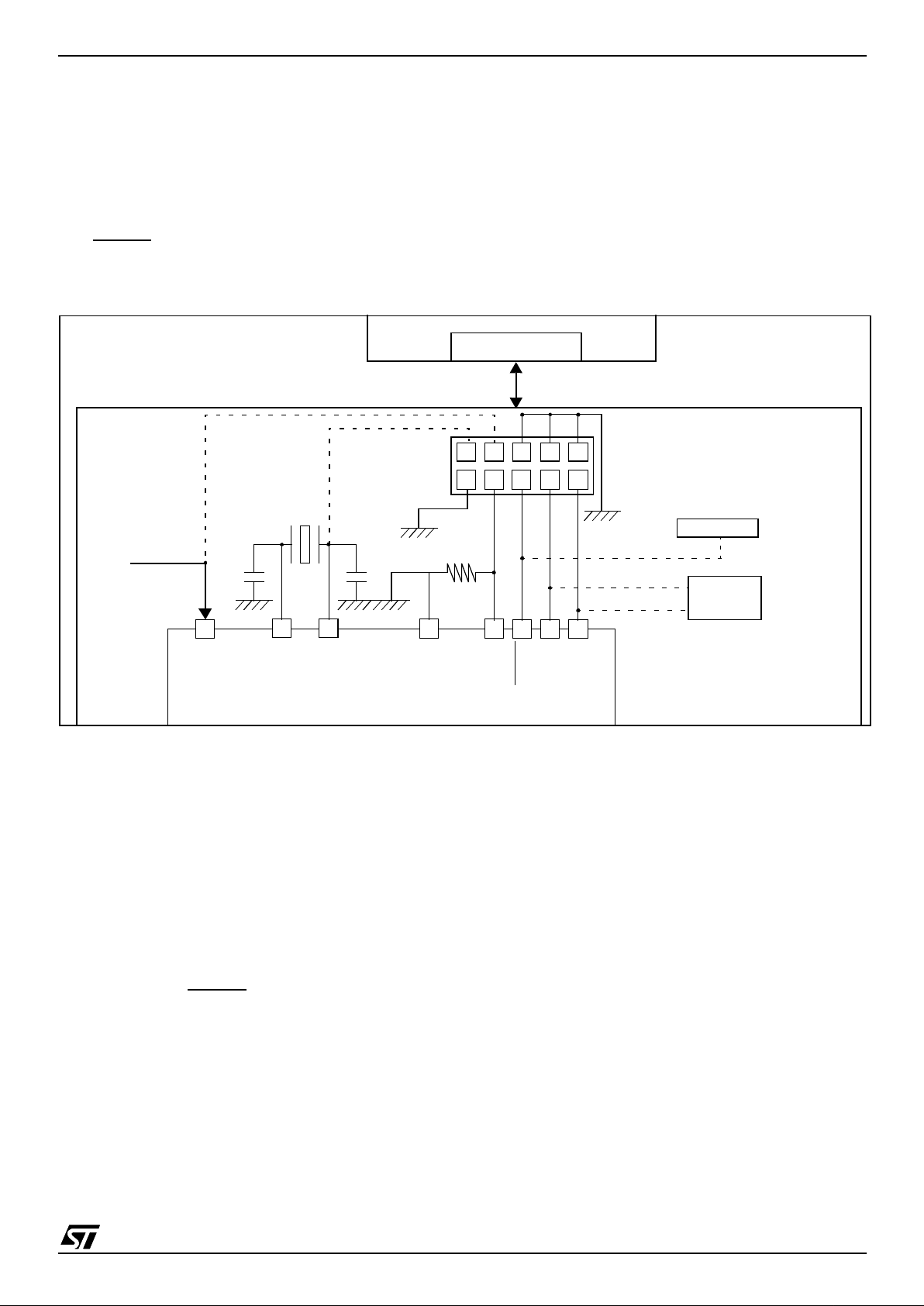
4.4 ICC Interface
ICC needs a m inimum of 4 and up to 6 pins to b e
connected to the programming tool (see Figure 6).
These pins are:
– RESET
: device reset
–V
SS
: device power supply ground
– ICCCLK: ICC output serial clock pin
– ICCDATA: ICC input/output serial data pin
– ICCSEL/V
PP
: programming voltage
– O SC1(or OSCIN): main clock in put for exter-
nal source (optional)
–V
DD
: application board power su pply (option-
al, see Figure 6, Note 3)
Figure 6. Typical ICC Interface
Notes:
1. If the ICCCLK or ICCDATA pins are only u sed
as outputs in t he ap plication, n o s ign al iso lation is
necessary. As soon as the Programming Tool is
plugged to the board, even if an ICC session is not
in progress, the ICCCLK and ICCDATA pins are
not available for the application. If they are used as
inputs by the application, isolation such as a serial
resistor has to implemented in case another device forces the signal. Refer to the Programming
Tool documentation for recommended resistor values.
2. During the ICC session, the programming tool
must control the RESET
pin. This can lead to conflicts between the programming tool and the application reset circuit if it drives more than 5mA at
high level (push pull output or pull-up resistor<1K).
A schottky diode can be us ed to iso late the application RESET circuit in this case. When using a
classical RC network with R>1K or a reset man-
agement IC with open drain ou tput and pu ll-up resistor>1K, no additional com ponents are needed.
In all cases the user must ensure that no external
reset is generated by the application during the
ICC session.
3. The use of Pin 7 of the ICC con nector de pends
on the Programming Tool architecture. This pin
must be connected when using most ST Programming Tools (it is used to monitor the application
power supply). Please refer to the Programming
Tool manual.
4. Pin 9 has to be co nnected to the OS C1 or OSCIN pin of the ST7 when the clock is not available
in the application or if the sel ected clock opt ion is
not programmed in t he option byte. ST7 devices
with multi-oscillator capability need to have OSC2
grounded in this case.
ICC CONNECTOR
ICCDATA
ICCCLK
RESET
V
DD
HE10 CONNECTOR TYPE
APPLICATION
POWER SUPPLY
1
246810
975 3
PROGRAMMING TOOL
ICC CONNECTOR
APPLICATION BOARD
ICC Cab le
OPTIONAL
(See No te 3)
10k
Ω
V
SS
ICCSEL/VPP
ST7
C
L2
C
L1
OSC1
OSC2
OPTIONAL
See Note 1
See Note 2
APPLICATION
RESET SOURCE
APPLICATI ON
I/O
(See No te 4)

ST72521
20/211
FLASH PROGRAM MEMORY (Cont’d)
4.5 ICP (In-Circuit Programming)
To perform ICP the microcontroller must be
switched to ICC (In-Circuit Communication) mode
by an external controller or programming tool.
Depending on the ICP code dow nloaded in RAM,
Flash memory programming can be fully customized (number of bytes to prog ram, program locations, or selection serial communication interface
for downloading).
When using an STMicroelectronics or third-party
programming tool that supp orts ICP and the specific microcontroller device, the user needs only to
implement the ICP hardware interface on the application board (see Figure 6). For more details on
the pin locations, refer to the device pinout description.
4.6 IA P ( I n-Appl i cation Pr ogramming)
This mode uses a BootLoader program previously
stored in Sector 0 by the us er (in ICP mode or by
plugging the device in a programming tool).
This mode is fully controlled by user software. This
allows it to be adapted to the user application, (user-defined strategy for entering programming
mode, choice of comm unications protocol used to
fetch the data to be stored, etc.). For example, it is
possible to download code from the SPI, SCI, USB
or CAN interface and program it in the Flash. IAP
mode can be used to program any of the Flash
sectors except Sector 0, whi ch is write/erase protected to allow recovery in case errors occur during the programming operation.
4.7 Related Documentation
For details on Flash program ming and ICC protocol, refer to the ST7 Flash Programming Reference Manual and to the ST7 ICC Protocol Re ference Manual
.
4.7.1 Register Description
FLASH CONTROL/STATUS REGISTER (FCSR)
Read/Write
Reset Value: 0000 0000 (00h)
This register is reserved for use by Programming
Tool software. It controls the Flash programming
and erasing operations. Flash Control/Status Register Address and Reset Value
70
00000000
Address
(Hex.)
Register
Label
76543210
0029h
FCSR
Reset Value00000000
ST72521
21/211
5 CENTRAL PRO CESSING UNIT
5.1 INTRODUCTION
This CPU has a full 8-bit architecture and contains
six internal registers allowing efficient 8-bit data
manipulation.
5.2 MAIN FEATURES
■ Enable executing 63 basic instructions
■ Fast 8-bit by 8-bit multiply
■ 17 main addressing modes (with indirect
addressing mode)
■ Two 8-bit index registers
■ 16-bit stack pointer
■ Low power HALT and WAIT modes
■ Priority maskable hardware interrupts
■ Non-maskable software/hardware interrupts
5.3 CPU REGISTERS
The 6 CPU registers shown in Figure 7 are not
present in the memory mapping and are accessed
by spec ifi c ins t ru c tio n s .
Accumulator (A)
The Accumulator is an 8-bit general purpose register used to hold operands and the res ults of the
arithmetic and logic calculations and to manipulate
data.
Index Registers (X and Y)
These 8-bit registers are used to create effective
addresses or as tempo rary storage areas f or data
manipulation. (The Cross -Assembler generates a
precede instruction (PRE) to indicate that the following instruction refers to the Y register.)
The Y register is not affected by the interrupt automatic procedures.
Program Counter (PC)
The program counter is a 16-bit register containing
the address of the next instruction to be executed
by the CPU. It is made of two 8-bit registers PCL
(Program Counter Low which is the LSB) and PCH
(Program Counter High which is the MSB).
Figure 7. CPU Registers
ACCUMULATOR
X INDEX REGISTER
Y INDEX REGISTER
STACK POINTER
CONDITION CODE REGISTER
PROGRAM COUNTER
70
1C1I1HI0NZ
RESET VALUE = RESET VECTOR @ FFFEh-FFFFh
70
70
70
0
7
15 8
PCH
PCL
15
8
70
RESET VALUE = STACK HIGHER ADDRESS
RESET VALUE =
1X11X1XX
RESET VALUE = XXh
RESET VALUE = XXh
RESET VALUE = XXh
X = Undefined Value
ST72521
22/211
CENTRAL PROC ESSING UNIT (Cont’d)
Condition Code Register (CC)
Read/Write
Reset Value: 111x1xxx
The 8-bit Condition Code regist er contains the i nterrupt masks and four flags representative of the
result of the instruction just executed. This register
can also be handled by the PUSH and POP instructions.
These bits can be individually tested and/or controlled by specific instructions.
Arithmetic Management Bits
Bit 4 = H
Half carry
.
This bit is set by hardware when a carry occurs between bits 3 and 4 of t he ALU during an ADD or
ADC instructions. It is reset by hardware during
the same instructio n s.
0: No half carry has occurred.
1: A half carry has occurred.
This bit is tested using the JRH or JRNH instruction. The H bit is useful in BCD arithmetic subroutine s .
Bit 2 = N
Negative
.
This bit is set and cleared by hardware. It is representative of the result sign of the last arithmetic,
logical or data manipulation. I t’s a copy of the result 7
th
bit.
0: The result of the last operation is positive or null.
1: The result of the last operation is negative
(i.e. the most significant bit is a log ic 1).
This bit is accesse d by the JRMI and JRPL instructions.
Bit 1 = Z
Zero
.
This bit is set and cleared by hardware. This bit indicates that the result of the last arithmetic, logical
or data manipulation is zero.
0: The result of the last operation is different from
zero.
1: The result of the last operation is zero.
This bit is accessed by the JREQ and JRNE test
instructions.
Bit 0 = C
Carry/borrow.
This bit is set and cleared b y hardware and software. It indicates an overflow or an un derflow has
occurred during the last arithmetic operation.
0: No overflow or underflow has occurred.
1: An overflow or underflow has occurred.
This bit is driven by the SCF and RCF instructions
and tested by the JRC and JRNC instructions. It i s
also affected by the “bit test and branch”, shift and
rotate instructions.
Interrupt Managem ent B i ts
Bit 5,3 = I1, I0
Interrupt
The combination of the I1 and I0 bits gives the current interrupt software priority.
These two bits are set/cleared by hardware when
entering in interrupt. The loaded value is given by
the corresponding bits in the interrupt software priority registers (IxSPR). They can be also set/
cleared by software with the RIM, SIM, IRET,
HALT, WFI and PUSH/POP instructions.
See the interrupt management chapter for more
details.
70
11I1HI0NZ
C
Interrupt Software Priorit y I1 I0
Level 0 (main) 1 0
Level 1 0 1
Level 2 0 0
Level 3 (= interrupt disable) 1 1
ST72521
23/211
CENTRAL PROC ESSING UNIT (Cont’d)
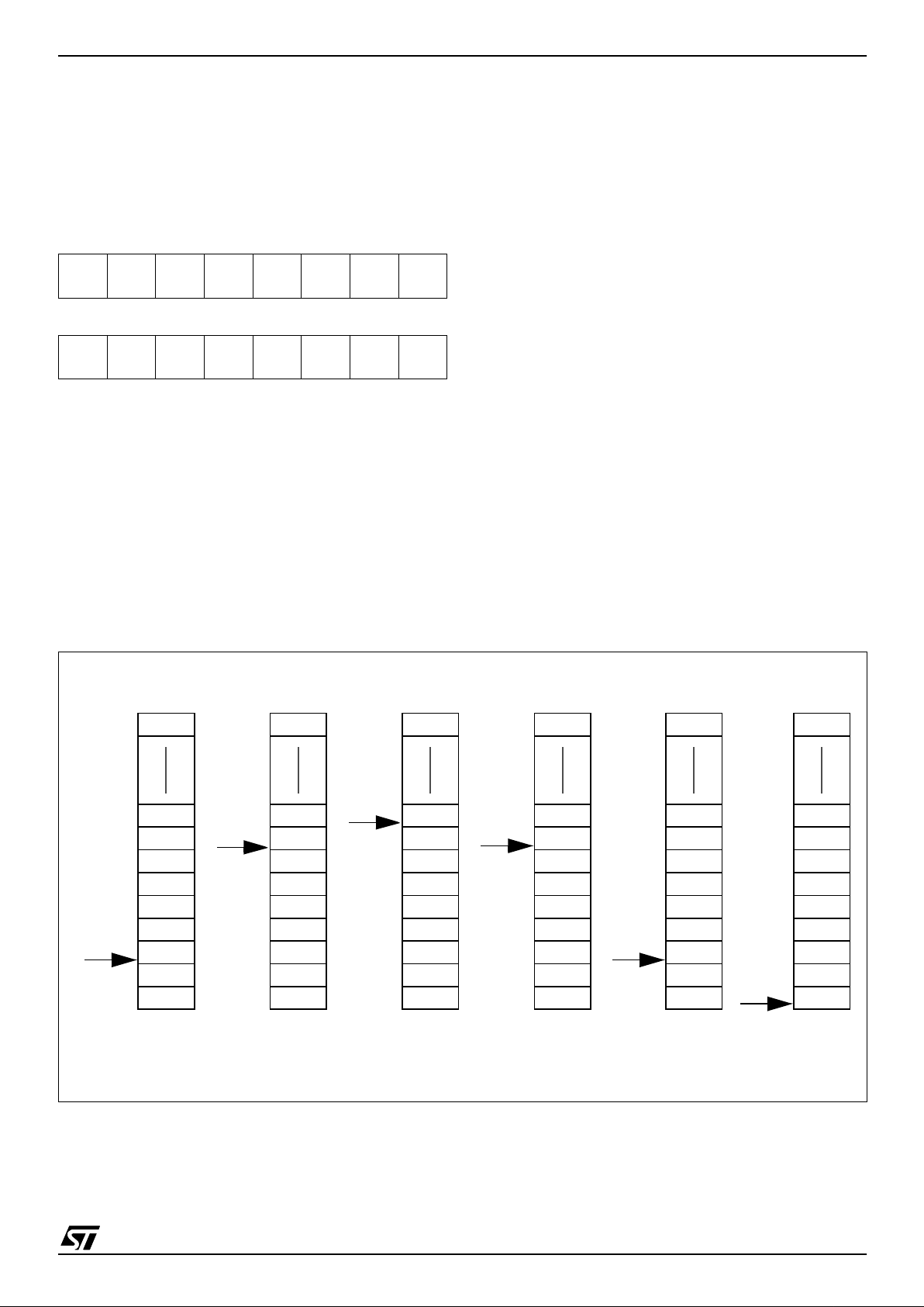
Stack Poi nter (SP)
Read/Write
Reset Value: 01 FFh
The Stack Pointer is a 16-bit register which is always pointing to the next free location in the stack.
It is then decremented after data has been pushed
onto the stack and incremented before data is
popped from the stack (see Figure 8).
Since the stack is 256 bytes deep, the 8 most significant bits are forced by hard ware. Following a n
MCU Reset, or after a Reset Stack Pointer instruction (RSP), the Stack Pointer contains its reset value (the SP7 to SP0 bits are set) which is the stack
higher address.
The least significant byte of the Stack Pointer
(called S) can be directly accessed by a LD instruction.
Note: When the lower limit is exceeded, the Stack
Pointer wraps around to the stack upper limit, without indicating the stack overflow. The previously
stored information is then o verwritten and therefore lost. The stack also wraps in case of an underflow.
The stack is used to sav e the return address during a subroutine call and the CPU context during
an interrupt. The user may also directly manipulate
the stack by means of the PUSH and POP instructions. In the case of an interrupt, the PCL is stored
at the first location po inted t o by t he SP. Th en t he
other registers are stored in the next locations as
shown in Figure 8.
– When an interrupt is received, the SP is decre-
mented and the context is pushed on the stack.
– On return from interrupt, the SP is incremented
and the context is popped from the stack.
A subroutine call occupies two locations and an interrupt five locat ion s i n the stack ar ea.
Figure 8. Stack Manipulation Example
15 8
00000001
70
SP7 SP6 SP5 SP4 SP3 SP2 SP1
SP0
PCH
PCL
SP
PCH
PCL
SP
PCL
PCH
X
A
CC
PCH
PCL
SP
PCL
PCH
X
A
CC
PCH
PCL
SP
PCL
PCH
X
A
CC
PCH
PCL
SP
SP
Y
CALL
Subroutine
Interrupt
Event
PUSH Y POP Y IRET
RET
or RSP
@ 01FFh
@ 0100h
Stack Higher Address = 01FFh
Stack Lower Address =
0100h
ST72521
24/211
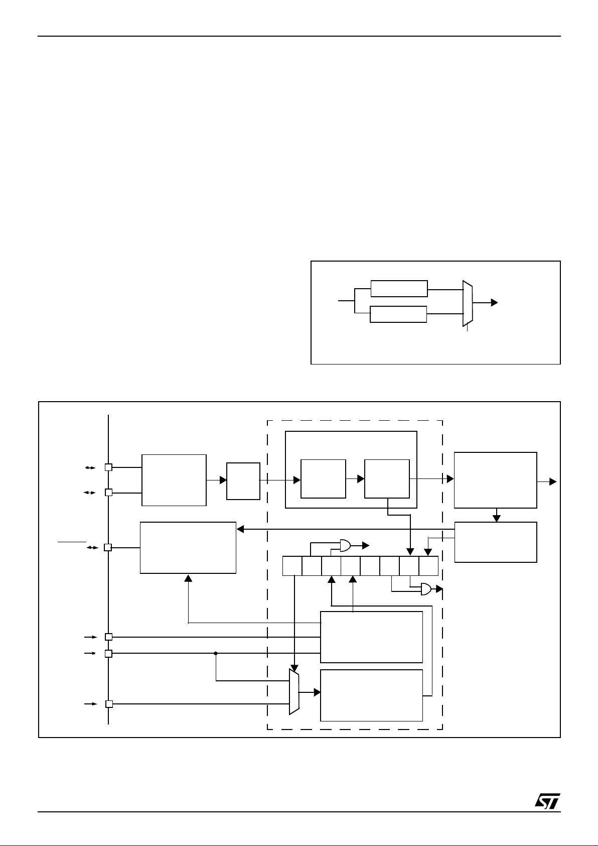
6 SUPPLY, RESET AND CLOCK MANAGEMENT
The device includes a range of utility features for
securing the application in critical situations (for
example in case of a power brown-out), and reducing the number of external components. An
overview is shown in Figure 10.
For more details, refer to dedicated parametric
section.
Main features
■ Optional PLL for multiplyi ng the frequency by 2
(not to be used with internal RC oscillator)
■ Reset Sequence Manager (RSM)
■ Multi-Oscillator Clock Management (MO)
– 5 Crysta l/ C er amic resonator osc illat o r s
– 1 Interna l RC o s c illat o r
■ System Integrity Management (SI)
– Main supply Low voltage detection (LVD)
– Auxiliary Voltage detector (AVD) with interrupt
capability for monitoring the main supply or
the EVD pin
– Clock Security System (CSS) with Clock Fil ter
and Backup Safe Oscillator (enabled by op-
tion byte)
6.1 PHASE LOCKED LOOP
If the clock frequency input to the PLL is in the
range 2 to 4 MHz, the PLL can be used to multiply
the frequency by two to obtain an f
OSC 2
of 4 to 8
MHz. The PLL is enabled by option byte. If the PLL
is disabled, then f
OSC2 = fOSC
/2.
Caution: T he PLL is not rec ommended for ap plications where timing accuracy is required. See
“PLL Characteristics” on page 176.
Figure 9. PLL Block Diagram
Figure 10. Clock, Reset and Supply Block Diagram
0
1
PLL OPTION BIT
PLL x 2
f
OSC2
/ 2
f
OSC
LOW VOLTAG E
DETECTOR
(LVD)
f
OSC2
AUXILIARY VOLTAGE
DETECTOR
(AVD)
MULTI-
OSCILLATOR
(MO)
OSC1
RESET
V
SS
EVD
V
DD
RESET SEQUENCE
MANAGER
(RSM)
CLOCK
FILTER
SAFE
OSC
CLOCK SECURITY SYSTEM
(CSS)
OSC2
MAIN CLOCK
CSS Interrupt Reque st
AVD Interrupt Request
CONTR O LLER
PLL
SYSTEM INTEGRITY MANAGEMENT
WATCHDOG
SICSR
TIMER (W DG )
WITH REALTIME
CLOCK (MCC/RTC)
AVDAVD AVD
LVD
RF
CSS
IEIE
CSSDWDG
RF
0
1
f
OSC
f
OSC2
(option)
0
SF
f
CPU
ST72521
25/211
6.2 MULTI-OSCILLATOR (MO)
The main clock of the ST7 can be generated by
th ree dif feren t sou rce types comin g fro m the multioscillator block:
■ an external source
■ 4 crystal or ceramic resonator oscillators
■ an internal high frequency RC oscillator
Each oscillator is optimized for a given freq uency
range in terms of consumption and is selectable
through the option byte. The assoc iated hardware
configurations are shown in Table 4. Refer to the
electrical characteristics section for more details.
Caution: T he OS C1 and/o r OSC2 pins mus t not
be left unconnected. F or the purpos es of Failure
Mode and Effect Analysis, it should be noted that if
the OSC1 and/or OSC2 pins are left unconnected,
the ST7 main osc illator m ay sta rt an d, in this configuration, could generate an f
OSC
clock frequency
in excess of the allowed maximum (>16MHz.),
putting the ST7 in an unsafe/undefined state. The
product behaviour must therefore be considered
undefined when the OSC pins are le ft unconnected.
External Clock Source
In this external clock mode, a clock signal (square,
sinus or triangle) with ~50% duty cycle has to drive
the OSC1 pin while the OSC2 pin is tied to ground.
Note: Ex ternal clock sou rce is not suppo rted with
the PLL enabled.
Crystal/Ceramic Oscillators
This family of oscillators has the advantage of producing a very accurate rate on the main clock of
the ST7. The s election within a list of 4 os cillators
with different frequency ran ges has to be done by
option byte in order to redu ce consumption (refer
to Se ction 14.1 on page 199 for more details on
the frequency ranges). In this mode o f the m ultioscillator, the resonator and the load capacitors
have to be placed as close as possible to the oscillator pins in order to minimize output distortion and
start-up stabilization time. The loading capacitance values must be adjusted according to the
selected osci lla tor .
These oscillators are not stopped during the
RESET phase to avoid losing time in the oscillator
start-up phase.
Internal RC Oscillator
This oscillator allows a low cost solution for the
main clock of the ST7 using only an internal resistor and capac it or. Int ernal RC oscillator mode has
the drawback of a lower frequency accuracy and
should not be used in applications that require accurate timin g .
In this mode, the two oscillator pins have to be tied
to ground.
Table 4. ST7 Clock Sources
Hardware Configuration
External ClockCrystal/Ceramic ResonatorsInternal RC Oscillator
OSC1 OSC2
EXTERNAL
ST7
SOURCE
OSC1 OSC2
LOAD
CAPACITORS
ST7
C
L2
C
L1
OSC1 OSC2
ST7
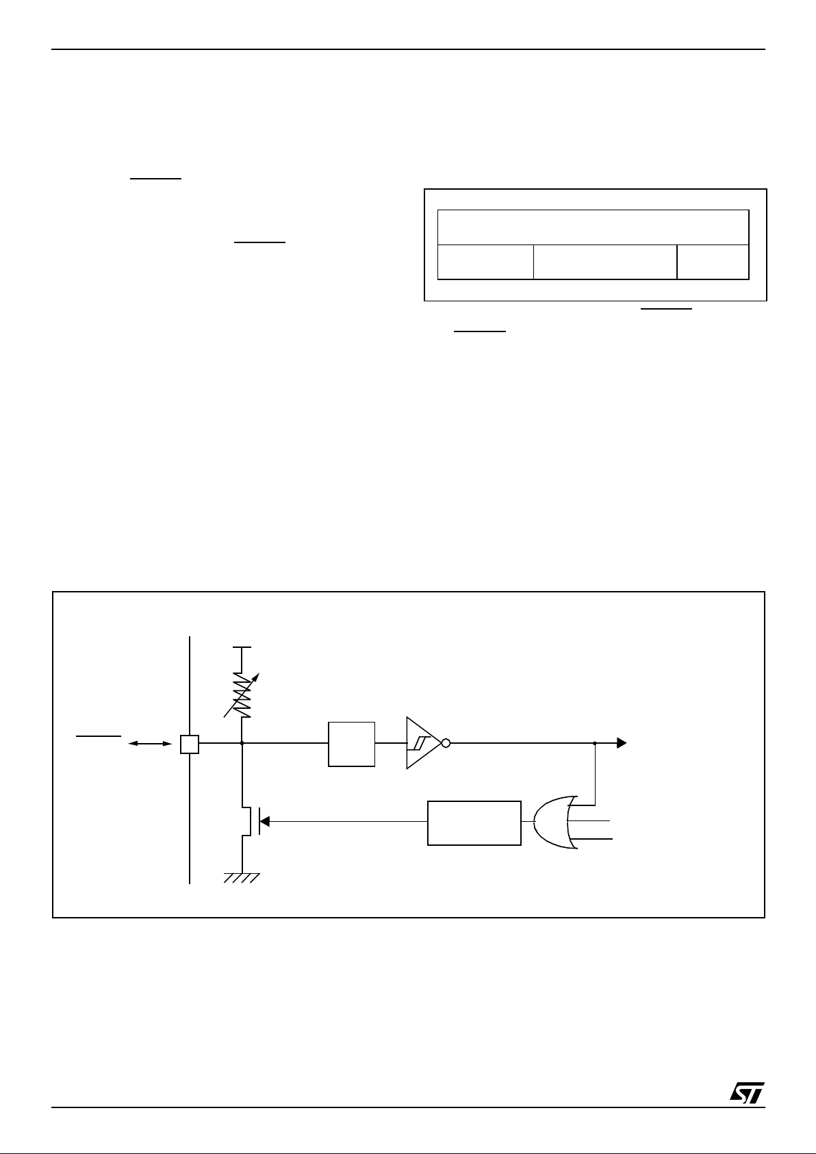
ST72521
26/211
6.3 RESET SEQUENCE MANAGER (RSM)
6.3.1 Introd uc tion
The reset sequence manager in cludes three RESET sources as shown in Figure 12:
■ External RESET source pulse
■ Internal LVD RESET (Low Voltage Detection)
■ Internal WATCHDOG RESET
These sources act on the RESET
pin and it is al-
ways kept low during the delay phase.
The RESET service routine vector is fixed at ad-
dresses FFFEh-FFFFh in the ST7 memory map.
The basic RE SET sequence consists of 3 phases
as shown in Figure 11:
■ Active Phase depending on the RESET source
■ 256 or 4096 CPU clock cycle delay (selected by
opt ion byt e)
■ RESET vector fetch
The 256 or 4096 CPU clock cycle delay allows the
oscillator to stabilise and ensures that recovery
has taken place from t he Reset st ate. T he short er
or longer clock cycle delay should be selected by
option byte to correspond to the stabilization t ime
of the external oscillator used in the application
(see Section 14.1 on page 199).
The RESET vector fetch phase duration is 2 clock
cycles.
Figure 11. RESET Sequence Phases
6.3.2 Async hr onous External RESET
pin
The RESET
pin is both an input and an open-drain
output with integrated R
ON
weak pull-up resistor.
This pull-up has no fixed value but varies in accordance with the input voltage. It
can be pulled
low by external circuitry to reset the dev ice. See
“CONTROL PIN CHARACTERISTICS” on
page 186 for more details.
A RESET signal originating from an external
source must have a duration of at least t
h(RSTL)in
in
order to be recognized (see Figure 13). This detection is asynchronous and therefore the MCU
can enter reset state even in HALT mode.
Figure 12. Reset Block Diagram
RESET
Active Phase
INTERNAL RESET
256 or 4096 CLOCK CYCLES
FETCH
VECTOR
RESET
R
ON
V
DD
WATCHDOG RESET
LVD RESET
INTERNAL
RESET
PULSE
GENERATOR
Filter
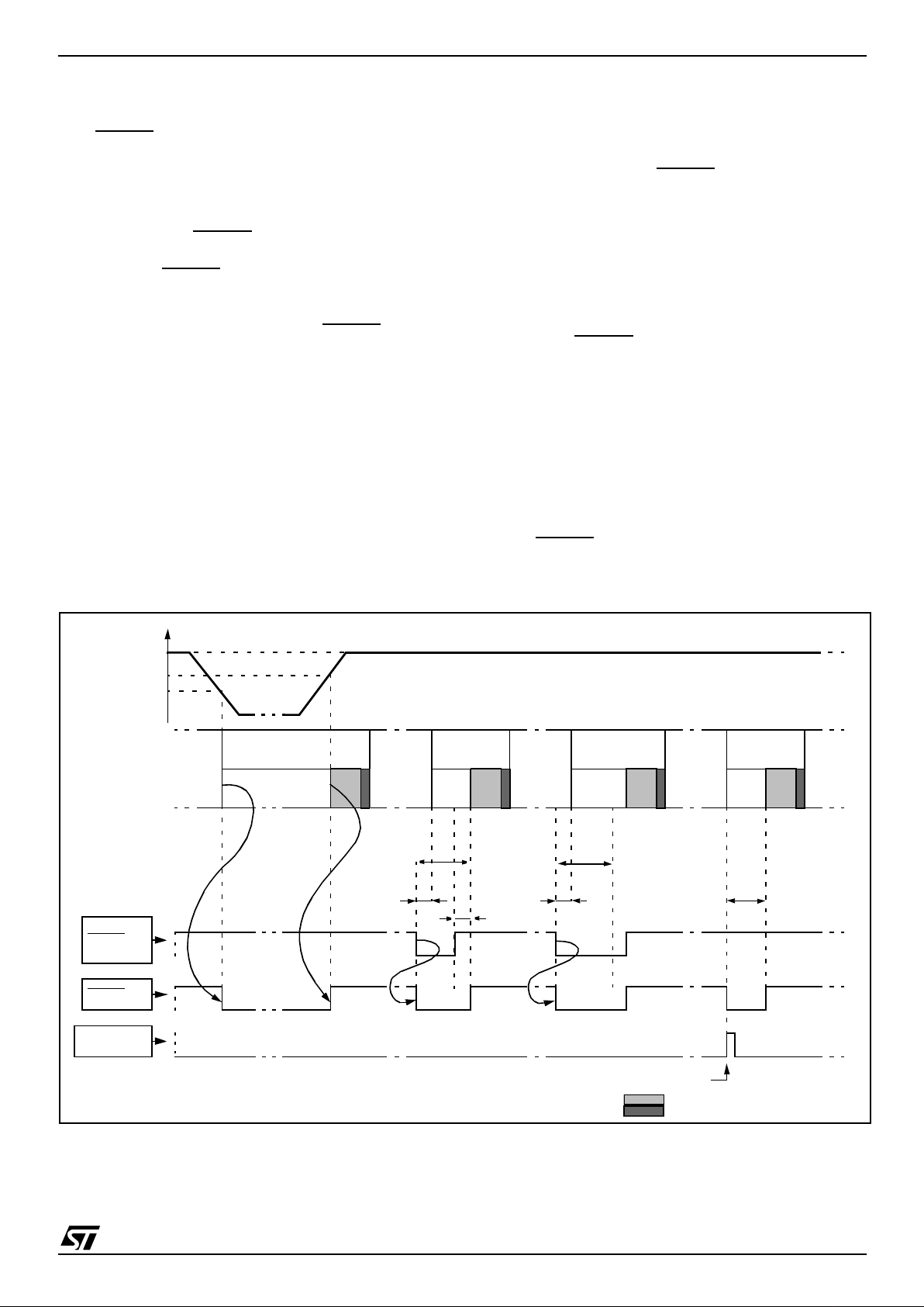
ST72521
27/211
RESET SEQUENCE MANAGER (Cont’d)
The RESET
pin is an asynchronous signal which
plays a major role in EMS performance. In a noisy
environment, it is recommended to follow the
guidelines mentioned in the elect rical characteristics section.
If the external RESET
pulse is shorter than
t
w(RSTL)out
(see short ext. Reset in Figure 13), the
signal on the RESET
pin may be stretched. Otherwise the delay will not be applied (see long ext.
Reset in Figure 13). Starting from the external RESET pulse recognition, the device RESET
pin acts
as an output that is pulled low during at least
t
w(RSTL)out
.
6.3.3 External Power-On RESET
If the LVD is disabled by option byte, to start up the
microcontroller correctly, the user must ensure by
means of an external reset circuit that the reset
signal is held low until V
DD
is over the minimum
level specified for the selected f
OSC
frequency.
(see “OPE RA TING CONDITIONS” on page 164)
A proper reset signal for a sl ow rising V
DD
supply
can generally be p rovided by an e xternal RC ne twork connected to the RESET
pin.
6.3.4 Internal Low Voltage Detector (LVD)
RESET
Two differe nt RESET sequences caused by the internal LVD circuitry can be distinguished:
■ Power-On RESET
■ Voltage Drop RESET
The device RESET
pin acts as an output that is
pulled low when V
DD<VIT+
(rising edge) or
V
DD<VIT-
(falling edge) as shown in Figure 13.
The LVD filters spikes on V
DD
larger than t
g(VDD)
to
avoid parasitic resets.
6.3.5 Internal Watchdog RESET
The RESET sequence generated by a internal
Watchdog counter overflow is shown in Figure 13.
Starting from the Watchdog counter underflow, the
device RESET
pin acts as an output that is pulled
low during at least t
w(RSTL)out
.
Figure 13. RESET Sequences
V
DD
RUN
RESET PIN
EXTERNAL
WATCHDOG
ACTIVE PHASE
V
IT+(LVD)
V
IT-(LVD)
t
h(RSTL)in
t
w(RSTL)out
RUN
t
h(RSTL)in
ACTIVE
WATCHDOG UNDERFLOW
t
w(RSTL)out
RUN RUN RUN
RESET
RESET
SOURCE
SHORT EXT.
RESET
LVD
RESET
LONG EXT.
RESET
WATCHDOG
RESET
INTE RNAL R ESET (256 or 40 96 T
CPU
)
VECTOR FETCH
t
w(RSTL)out
PHASE
ACTIVE
PHASE
ACTIVE
PHASE
DELAY
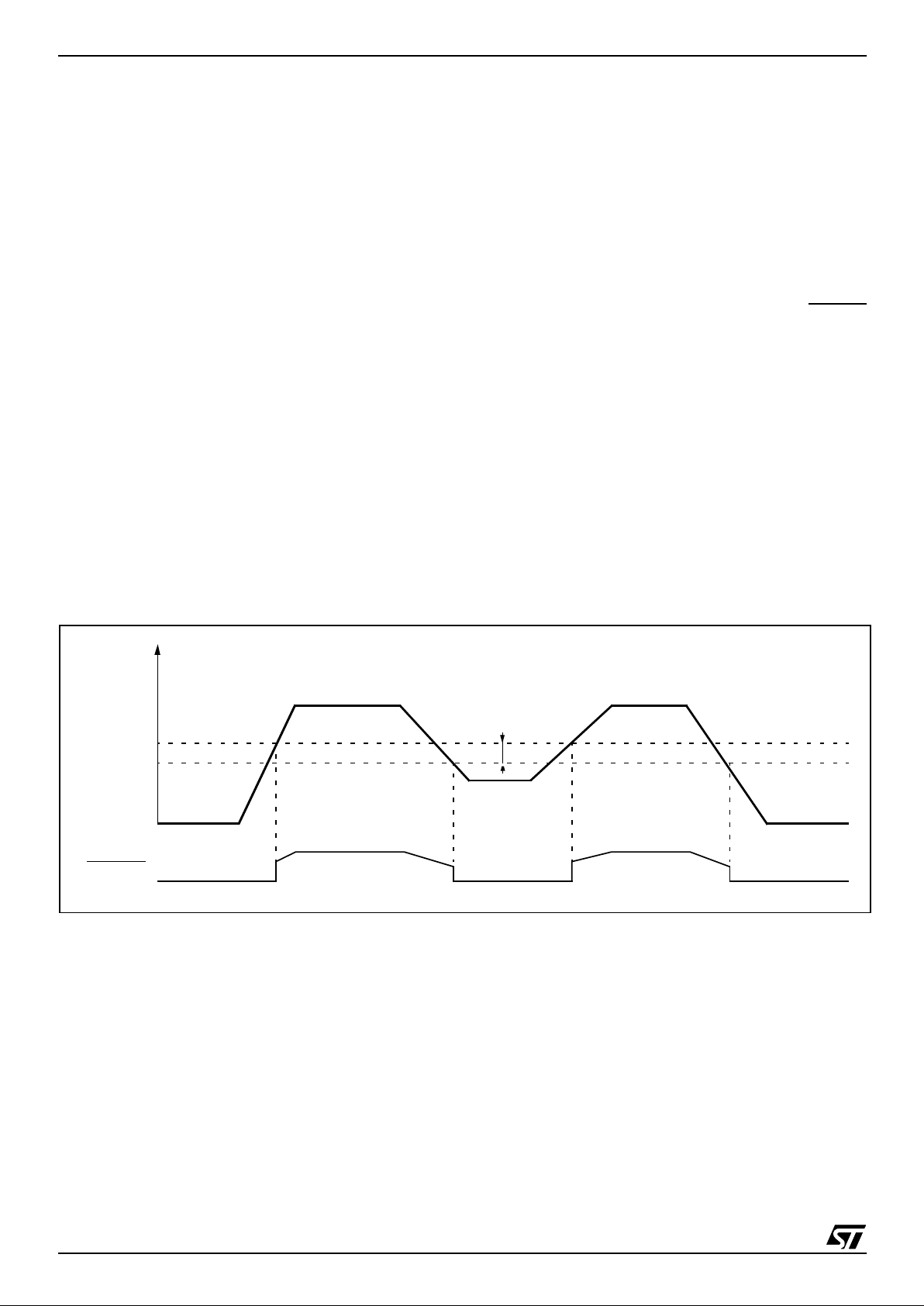
ST72521
28/211
6.4 SYSTEM INTEGRITY MANAGEMENT (SI)
The System Integrity Mana gement block co ntains
the Low Voltage Detector (LVD), Auxiliary Voltage
Detector (AVD) functions and Clo ck Security System (CSS). It is managed by the SICSR register.
6.4.1 Low Voltage Detector (LVD)
The Low Voltage Dete ctor funct ion (LVD) generates a static reset when the V
DD
supply voltage is
below a V
IT-
reference value. This means that it
secures the power-up as well as the power-dow n
keeping the ST7 in reset.
The V
IT-
reference value for a voltage drop is lower
than the V
IT+
reference value for power-on in order
to avoid a parasitic reset when the MCU starts running and sinks current on the supply (hysteresis).
The LVD Reset circuitry generat es a reset when
V
DD
is below:
–V
IT+
when VDD is rising
–V
IT-
when VDD is falling
The LVD func t io n is illustrat ed in F igure 14.
Provided the minimum V
DD
value (guaranteed for
the oscillator frequency) is above V
IT-
, the MCU
can only be in two modes:
– under full software control
– in static safe reset
In these conditions, secure operation is always ensured for the application without the need for external reset hardware.
During a Low Voltage Detector Reset, the RESET
pin is held low, thus p ermitting the MCU to reset
other devices.
Notes:
The LVD allows the device to be used without any
external RESET circuitry.
If the medium or low thresholds are selected, the
detection may occur outside the specified operating voltage range. Below 3.8V, device operation is
not guaranteed.
The LVD is an optional func tion which can be selected by option byte.
Figure 14. Low Voltage Detector vs Reset
V
DD
V
IT+
RESET
V
IT-
V
hys
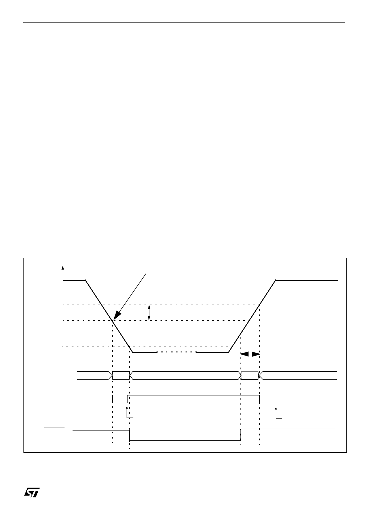
ST72521
29/211
SYSTEM INTEGRITY MANAGEMENT (Cont’d)
6.4.2 Auxiliary Voltage Detector (AVD)
The Voltage Detector function (AVD) is based on
an analog comparison between a V
IT-(AVD)
and
V
IT+(AVD)
reference value and the VDD main sup-
ply or the external EVD pin voltage level (V
EVD
).
The V
IT-
reference value for falling voltage is lower
than the V
IT+
reference value for rising voltage in
order to avoid parasitic detection (hysteresis).
The output of the AVD comparator is directly read-
able by the application software through a real
time status bit (AVDF) in t he S ICS R regi ster. This
bit is read only.
Caution: The AVD function is active only if the
LVD is enabled through the option byte.
6.4.2.1 Monitoring the V
DD
Main Supp ly
This mode is selected by clearing the AVDS bit in
the SICSR register.
The AVD voltage threshold value is relative to the
selected LVD threshold configured by option byt e
(see Section 14.1 on page 199).
If the AVD interrupt is enabled, an interrupt is generated when the voltage crosses the V
IT+(AVD )
or
V
IT-(AVD)
threshold (AVDF bit toggles).
In the case of a drop i n v oltage, t he A V D i nterrupt
acts as an early warning, allowing software to shut
down safely before the LV D resets the microcontroller. See Figure 15.
The interrupt on the rising edge is used to info rm
the application that the V
DD
warning state is over.
If the voltage rise time t
rv
is less than 256 or 4 096
CPU cycles (depending on the reset delay selected by option byte), no AVD interrupt will be generated when V
IT+(AVD)
is reached.
If t
rv
is greater than 256 or 4096 cycles then:
– If the AVD interrupt is enabled before the
V
IT+(AVD)
threshold is reached, then 2 AVD interrupts will be received: the first when the AVDIE
bit is set, and the second when the threshold is
reached.
– If the AVD interrupt is enabled after the V
IT+(AVD)
threshold is reached then only one AVD interrupt
will occur.
Figure 15. Using the AVD to Monitor V
DD
(AVDS bit= 0)
V
DD
V
IT+(AVD)
V
IT-(AVD)
AVDF bit 0 0RESET VALUE
IF AVDIE bit = 1
V
hyst
AVD INTERRUPT
REQUEST
INTERRUPT PROCESS
INTERRUPT PROCESS
V
IT+(LVD)
V
IT-(LVD)
LVD RESET
Early Warning Interrupt
(Power has dropped, MCU not
not yet in reset)
1
1
t
rv
VOLTAGE RISE TIME
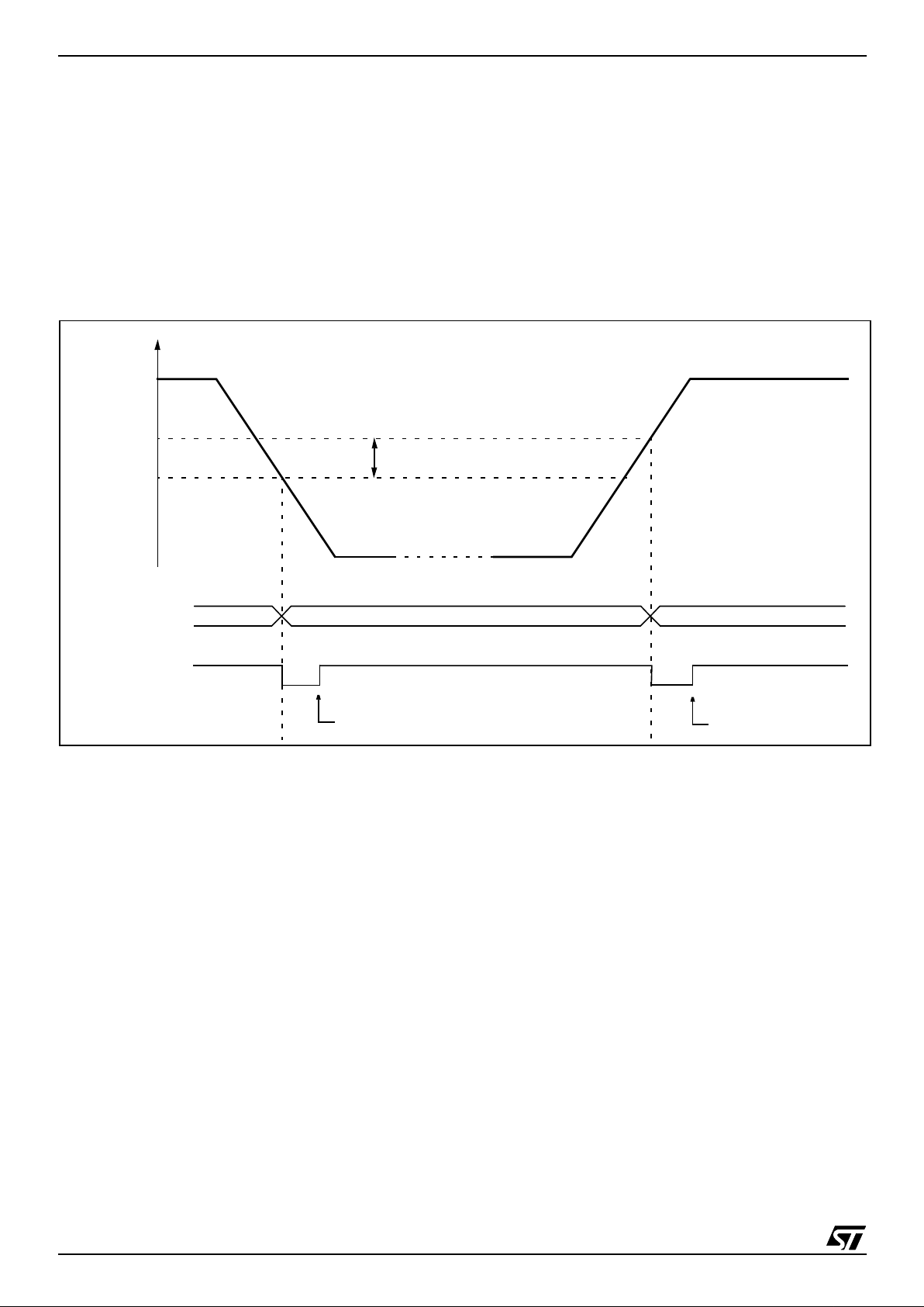
ST72521
30/211
SYSTEM INTEGRITY MANAGEMENT (Cont’d)
6.4.2.2 Monitoring a Voltage on the EVD pin
This mode is selected b y setting the AVDS bit in
the SICSR register.
The AVD circuitry can generate an interrupt when
the AVDIE bit of the SICSR register is set. This interrupt is generated on the rising and falling edges
of the comparator output. This means it is generated when either one of these two events occur:
–V
EVD
rises up to V
IT+(EVD)
–V
EVD
falls down to V
IT-(EVD)
The EVD func t io n is illustrat ed in Figure 16.
For more details, refer to t he E lectrical Ch aracter-
istics sect ion.
Figure 16. Using the Voltage Detector to Monitor the EVD pin (AVDS bit=1)
V
EVD
V
IT+(EVD)
V
IT-(EVD)
AVDF 0 01
IF AVDIE = 1
V
hyst
AVD INTERRUPT
REQUEST
INTERRUPT PROCESS
INTERRUPT PROCESS
 Loading...