

SGS Thomson Microelectronics ST72411R1, ST72411R Datasheet
Rev. 1.4
January 2000 1/71
ST72411R
8-BIT MCU WITH SMARTCARD INTERFACE, LCD DRIVER,
8-BIT TIMER, SAFE RESET AND SUPPLY MONITORING
PRODUCT PREVIEW
■ Memories
– 4K Program memory
(ROM/FLASH) with read-out protection
– In-Situ Programming (remote ISP) for FLASH
devices using Smartcard orstandard I/O lines
– 256-bytes RAM
■ Clock, Reset and Supply Management
– Power-on supply at Smartcard insertion
– Low supply voltage detection for battery
monitoring
– Smart Card withdrawal detection
– On-chip main clock source
– 3 Power saving modes
– Clock-out capability for synchronous and
asynchronous Smartcards
■ Smartcard Interface
– Smart Card Supply Supervisor with: 3V or 5V
voltage regulator and current overload protec-
tion
■ 15 I/O Ports
– 15 multifunctional bidirectional I/O lines with:
external interrupt capability (2 vectors), 2 al-
ternate function lines, 5 I/Os for ISO7816-3
Smartcard interface, 1 I/O for Smartcard with-
drawal detection
■ Display Driver
– LCD driver with 32 segment outputs and 4
backplane outputs able to drive up to 32x4
LCD displays
■ Timer
– One 8-bit timer with: 9-bit prescaler, selecta-
ble input frequency with external clock input
option and event output signal generation ca-
pability
■ Instruction Set
– 8-bit Data Manipulation
– 63 Basic Instructions
– 17 main Addressing Modes
– 8 x 8 Unsigned Multiply Instruction
– True Bit Manipulation
■ Development Tools
– Full hardware/software development package
Device Summary
TQFP64
14 x 14
Features ST72411R
Program memory - bytes 4K
RAM (stack) - bytes 256 (64)
Peripherals Smart Card supply interface, LCD Driver, 8-bit Timer
Operating Supply 4V to 6.6V (5.5V min. for 5V Smartcard power supply output)
CPU Frequency 3.58 MHz (7.16 MHz internal oscillator)
Temperature Range 0°C to +70°C
Packages TQFP64 or Die Form
Development device ST72C411R
1

Table of Contents
71
2/71
2
1 GENERAL DESCRIPTION . . . . . . ................................................ 4
1.1 INTRODUCTION . . . . . .. . . . . . ............................................. 4
1.2 PIN DESCRIPTION . . ..................................................... 5
1.3 REGISTER & MEMORY MAP . . . ............................................ 8
1.4 FLASH PROGRAM MEMORY . . . . . . . . . . . . .................................. 10
1.4.1 Introduction . . . .................................................... 10
1.4.2 Main features . . . . . . . . . . . . . . . . . . . . . .. . . . . . . . . . . . . . . . . . . . . . . . . . . . . . . . 10
1.4.3 Structural organisation . . . . . . . . . . . . . . ................................. 10
1.4.4 In-Situ Programming(ISP) modes . . . . . . . . . . . . . . . . . . .................... 10
1.5 PROGRAM MEMORY READ-OUT PROTECTION . . . . . . . . . . . . . . . . . . . ...........11
2 CENTRAL PROCESSING UNIT . . ............................................... 12
2.1 INTRODUCTION . . . . . .. . . . . . ............................................12
2.2 MAIN FEATURES . . . . . . . . . . . . . . . . . . . . . . . . . .............................. 12
2.3 CPU REGISTERS . . . .................................................... 12
3 SUPPLY, RESET AND CLOCK MANAGEMENT . . . . ................................ 15
3.1 LOW VOLTAGE DETECTOR AND SUPERVISOR (LVDS) . . . . . . . . . . . . . . . . . . . . . . . 15
3.1.1 Low Voltage Detector . . . . . ........................................... 15
3.1.2 Open Power Supply Detection (OPSD) . ................................. 15
3.1.3 Power Supply Supervisor (PSS) . . . .................................... 15
3.2 RESET SEQUENCE MANAGER . . . . . . . . . . . . . . . . . . . . . . . . . . . . . . . . . . . . . . . . . . . . 18
3.3 MAIN CLOCK CONTROLLER SYSTEM (MCC) . . . ............................. 21
4 INTERRUPTS . . ............................................................. 22
4.1 NON MASKABLE SOFTWARE INTERRUPT .................................. 22
4.2 EXTERNAL INTERRUPTS . . . . . . . . . . .. . . . . . ............................... 22
4.3 PERIPHERAL INTERRUPTS ............................................... 22
4.4 POWER SAVING MODES . . . . . . . . . . . . . . . . . . . . . . . . . . . . . . . . . . . . . . . . . ........ 25
4.4.1 Introduction . . . .................................................... 25
4.4.2 Slow Mode . . . . . . . . . . . . . . . . . . . . . . . ................................. 25
4.4.3 Wait Mode . . . . . . . . . . . . . . . . ........................................ 25
4.4.4 Halt Mode . . . . . .................................................... 26
5 ON-CHIP PERIPHERALS . . . . . . . . . . . ...........................................27
5.1 I/O PORTS . . . . . . . . . . . . . . . . . . ...........................................27
5.1.1 Introduction . . . .................................................... 27
5.1.2 Functional Description . . . . ........................................... 27
5.1.3 I/O Port Implementation . . . . . . . . . . . . . . . . . . . ........................... 29
5.1.4 Register Description . . . . . . ........................................... 30
5.2 MISCELLANEOUS REGISTER . . . . . . . . . . . .................................. 32
5.2.1 I/O Port Interrupt Sensitivity Description . . . . . . . . . . . . . . . . . . . . . . . . . . . .. . . . . 32
5.2.2 Slow modeand VDD Supply Monitoring .................................32
5.3 8-BIT TIMER (TIM8) . . . . . . . . . . . . . . . . . . . . . ................................. 34
5.3.1 Introduction . . . .................................................... 34
5.3.2 Main Features . . . . . . ...............................................34
5.3.3 Counter/Prescaler Description . . . . . . . . . . . . . . . . . . . . . . . . . . . . . . . . . ........ 35
5.3.4 Functional description . . . . . . . . . . . . . . . . . . . . ........................... 36
5.3.5 Register Description . . . . . . ........................................... 38

Table of Contents
3/71
3
5.4 32 X 4 LCD DRIVER . . . . . . . . . . ........................................... 40
5.4.1 Introduction . . . .................................................... 40
5.4.2 Segment and Common signals . . . . . . . . . . . . . . . . . . . . . . . . . . . . . . . . ........ 41
5.4.3 Reference Voltages . . . . . . . . . . . . . . . . ................................. 41
5.4.4 Display Example . . . . . . . . . . . ........................................ 41
5.4.5 Clock generation . . . . . . . . . . . . . . . . . . . . . . . . . .. . . . . . . . . . . . . . . . . . . . . . . . . 43
5.4.6 Register Description . . . . . . ........................................... 44
5.4.7 LCD RAM Description . .. . . . . . . . . . . . . . . . . . . . . . . . . . . . . . . . . . . . . . . . . . . . . 44
5.5 SMARTCARD SUPPLY SUPERVISOR (SSS) ................................. 46
5.5.1 Introduction . . . .................................................... 46
5.5.2 Main Features . . . . . . ...............................................46
5.5.3 General description . . . . . .. . . . . . . . . . . . . . . . . . . . . . . . . . . . . . . . . . . . . . . . . . . 46
5.5.4 Functional Description . . . . ........................................... 47
5.5.5 Register Description . . . . . . ........................................... 48
6 INSTRUCTION SET . . . . . . . . . . . . . . . . . . ........................................ 50
6.1 ST7 ADDRESSING MODES . . . . . . . . . . . . . . . . . . . . . . . . . . . . . . . . . . . . . . . . . . . . . . . 50
6.1.1 Inherent . . . . . . . . . . . ...............................................51
6.1.2 Immediate . . . . . . . . . . . . . . . . . . . . . . . . . . . . . . . . . . . . . . . . . . . . . . . . . . . . . . . . 51
6.1.3 Direct . ........................................................... 51
6.1.4 Indexed (No Offset, Short, Long) . . . . . . . . . . . . ........................... 51
6.1.5 Indirect (Short, Long) . . . . .. . . . . . . . . . . . . . . . . . . . . . . . . . . . . . . . . . . . . . . . . . . 51
6.1.6 Indirect Indexed (Short, Long) . ........................................ 52
6.1.7 Relative mode (Direct, Indirect) . . . . . . . . . . . . . . . . . . . . . . . . . . . . . . . . . . . . . . . . 52
6.2 INSTRUCTION GROUPS . . . . . . . . . . . . . . . . .................................53
7 ELECTRICAL CHARACTERISTICS . . . . . . . . . . . . . . . . .............................. 56
7.1 ABSOLUTE MAXIMUM RATINGS . . . ........................................ 56
7.2 RECOMMENDED OPERATING CONDITIONS . . . . . . . . . . . . . . . . . . . . . . . . . . . . . . . . 57
7.3 SUPPLY, RESET AND CLOCK CHARACTERISTICS . . . . . .. . . . . . . . . . . . . . . . . .... 60
7.4 TIMING CHARACTERISTICS . . ...........................................60
7.5 MEMORY CHARACTERISTICS . . . . . . . . . . . . . . . . . . . . . . . . . . . . . . . . . . . . . . . . . . . . 61
7.5.1 RAM and Hardware Registers . . . . . . . . . . . . . . . . . . . . . . . . . . . . . . . . ........ 61
7.5.2 FLASH Program Memory . ...........................................61
7.6 LCD ELECTRICAL CHARACTERISTICS . . . . . . . . . . . . . . . . . . . . . . ............... 61
7.7 SMARTCARD SUPPLY SUPERVISOR ELECTRICAL CHARACTERISTICS . . . . . . . . . . 62
8 DEVICE CONFIGURATION . . . . . ............................................... 64
8.1 OPTION BYTE . . . . . . . ................................................... 64
9 GENERAL INFORMATION . . . . . . . . . . ...........................................65
9.1 PACKAGE MECHANICAL DATA . . . . . . .. . . . . . . . . . ........................... 65
9.2 ADAPTOR / SOCKET PROPOSAL . . . . . . . . . . . . . . . . . . . . . . . . . . . . . . . . . . ........ 66
9.3 DEVELOPMENT TOOLS . . . . . . . . . . . . . . . . . . . . . . . . . . . . . . . . . . . . . . . . . . ........ 67
9.4 ST7 APPLICATION NOTES . . . . . . . ........................................ 68
9.5 TO GET MORE INFORMATION . . . . . . . . .................................... 68
10 SUMMARY OF CHANGES . ................................................... 69
10.1DEVICE CONFIGURATION AND ORDERING INFORMATION . . . . . ............... 70
10.1.1Transfer Of Customer Code . . . . . . . ....................................70
ST72411R
4/71
1 GENERAL DESCRIPTION
1.1 INTRODUCTION
The ST72411R devices are members of the ST7
microcontroller family. They are designed for
Smartcard reader applications.
All ST72411R family devices are based on a common industry-standard 8-bit core, featuring an enhanced instruction set.
The ST72C411R devices feature single-voltage
FLASH memory with byte-by-byte In-Situ Programming (ISP) capability.
Under software control, all devices can be placed
in WAIT, SLOW, or HALT mode, reducing power
consumption when the application is in idle or
standby state.
The enhanced instruction set and addressing
modes of the ST7 offer both power and flexibilityto
software developers, enabling the design ofhighly
efficient andcompact application code.In addition
to standard 8-bit data management, all ST7 microcontrollers feature true bit manipulation, 8x8 unsigned multiplication and indirect addressing
modes.
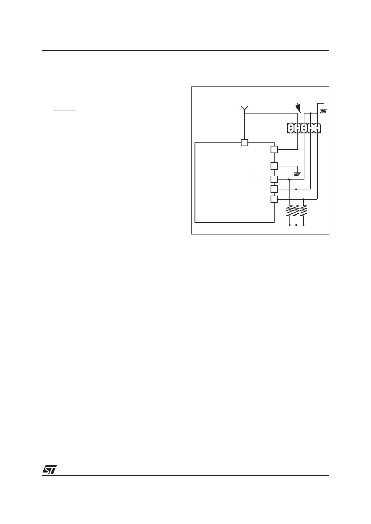
Figure 1. Device Block Diagram
8-BIT CORE
ALU
ADDRESS AND DATA BUS
OSC_SEL
CONTROL
PROGRAM
(4K Bytes)
V
SS
RESET
RAM
(256 Bytes)
PORT A
PA7:0
(8 bits)
8-BIT TIMER
PORT B
PB6:0
(7 bits)
V
DD
OSCIN
INTEGRATED
LVDS
MEMORY
7.16 MHZ
OSCILLATOR
SC SUPPLY
SUPERVISOR
SC_PWR
LCD DRIVER
+
LCD RAM (32x4)
SEG31:0
(32 segments)
COM3:0
(4 coms)
V
REF
(SSS)
4
ST72411R
5/71
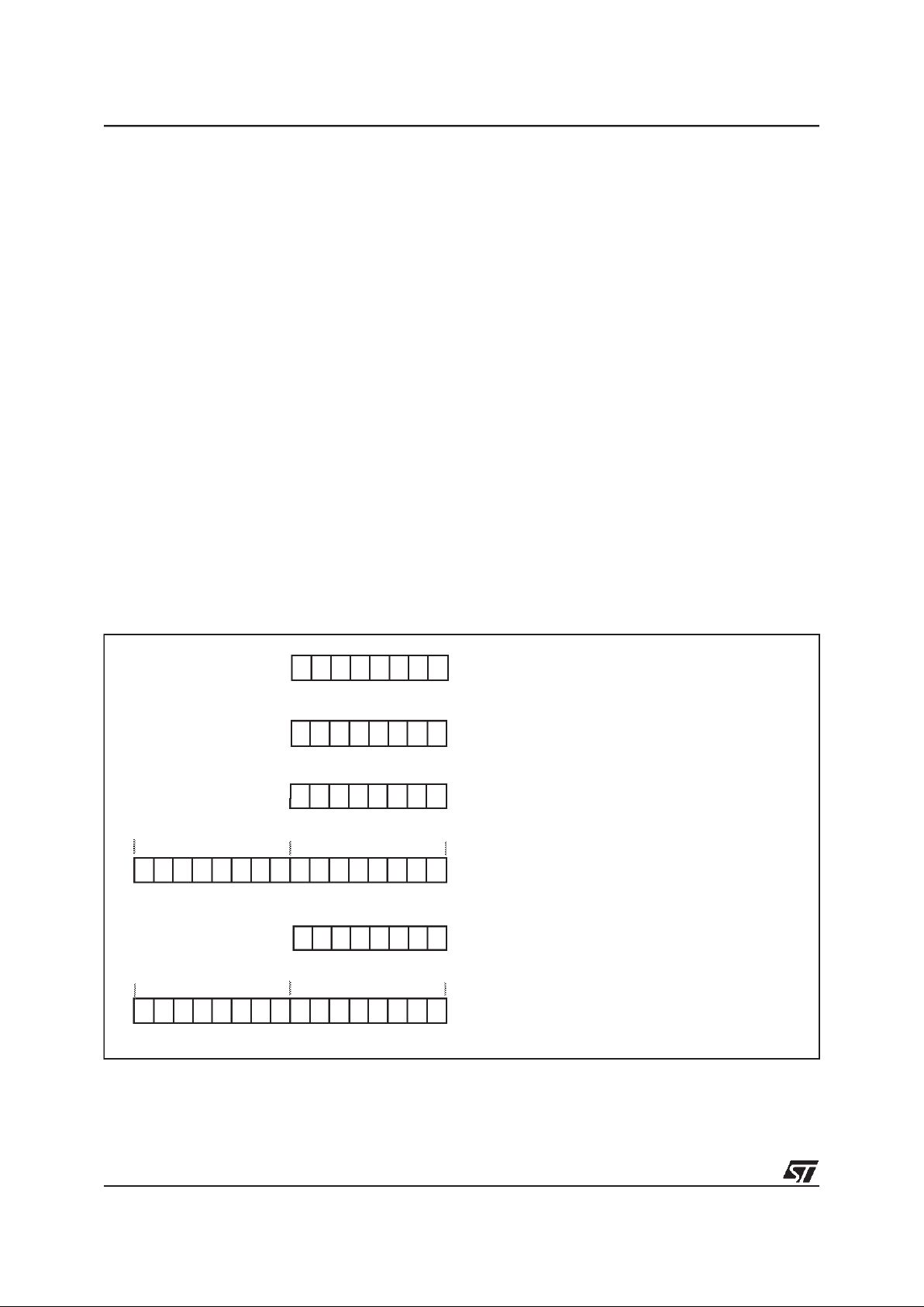
1.2 PIN DESCRIPTION
Figure 2. 64-Pin TQFP Package Pinout
(SC) PB4
(SC) PB3
ISPCLK1 / (SC_CK) PB2
ISPDATA1 / (SC_DATA) PB1
(SC_RESET) PB0
SC_PWR
V
DDA
V
DD
V
SSA
V
SS
OSCIN
NC
NC
V
REF
PB6
PB5
64 63 62 61 60 59 58 57 56 55 54 53 52 51 50 49
48
47
46
45
44
43
42
41
40
39
38
37
36
35
34
33
17 18 19 20 21 22 23 24 29 30 31 3225 26 27 28
1
2
3
4
5
6
7
8
9
10
11
12
13
14
15
16
EI0
RESET
ISP_SEL / OSC_SEL
PA7
NC
PA6
NC
PA5
PA4
PA3
ISPCLK2 / PA2
ISPDATA2 / PA1
TIMIO / PA0
SEG28
SEG29
SEG30
SEG31
SEG7
SEG6
SEG5
SEG4
SEG3
SEG2
SEG1
SEG0
COM3
COM2
COM1
COM0
SEG11
SEG10
SEG9
SEG8
SEG23
SEG22
SEG21
SEG20
SEG19
SEG18
SEG17
SEG16
SEG15
SEG14
SEG13
SEG12
SEG27
SEG26
SEG25
SEG24
EI1
EI0
EI0
5
ST72411R
6/71
PIN DESCRIPTION (Cont’d)
Legend / Abbreviations:
Type: I = input, O = output, S = supply
Output level: SC = powered by V
SC_PWR
smartcard power, HS = high sink (on N-buffer only)
Input level: C = CMOS : 0.3VDD/0.7VDD, SC = CMOS : 0.3V
SC_PWR
/ 0.7V
SC_PWR
Port configuration capabilities:
– Input:float = floating, wpu = weak pull-up, int = interrupt, wpd = weak pull-down
– Output: OD = open drain, T = true open drain, PP = push-pull
Note: Reset configuration of each pin is bold.
Table 1. Device Pin Description
Pin n°
Pin Name
Type
Level Port
Main
function
(after
reset)
Alternate function
TQFP64
Input
Output
Input Output
float
wpu
int
wpd
OD
PP
1 ... 4 S28 ... S31 O LCD Segment outputs
5 RESET I/O Top priority non maskable interrupt.
6 OSC_SEL / ISP_SEL I
This pin acts as the Remote ISP mode and
oscillator selection.
7 PA7 I/O C X EI0 X X Port A7
8 NC Not Connected
9 PA6 I/O C X EI0 X X Port A6
10 NC Not Connected
11 PA5 I/O C X EI0 X X Port A5
12 PA4 I/O C X EI0 X X Port A4
13 PA3 I/O C X EI0 X X Port A3
14 PA2 / ISPCLK2 I/O C X EI0 X X Port A2 ISP Clock line 2
15 PA1 / ISPDATA2 I/O C X EI0 X X Port A1 ISP Data line 2
16 PA0 / TIMIO I/O C X EI0 X X Port A0 8-bit Timer I/O
17 NC Not Connected
18 V
REF
1)
I Analog input for battery power monitoring
19 PB6 I/O C X EI1 X X Port B6
20 PB5 I/O C X EI1 X X Port B5
21 PB4(SC) I/O SC SC X EI1 X X Port B4 (Smartcard)
22 PB3(SC) I/O SC SC X EI1 X X Port B3 (Smartcard)
23
PB2(SC_CK) /
ISPCLK1
I/O SC SC X EI1 X X
Port B2 (Smartcard
clock)
ISP Clock line 1
24
PB1(SC_DATA) /
ISPDATA1
I/O SC SC
X
XX
Port B1 (Smartcard
Data)
ISP Data line 1
EI1
25 PB0(SC) I/O SC SC X EI1 X X Port B0 (Smartcard)
26 SC_PWR O Smartcard Regulated Supply Output
27 V
DDA
S Analog Power Supply Voltage
28 V
DD
S Digital Main Supply Voltage
ST72411R
7/71
Note:
1) There is no protection diode referenced to VDDon the V
REF
pad. If the microcontroller is not poweredon atthe main VDDsupply, it is possible tohave nopower consumption (other thanleakage currents -see
electrical parameters), while applying power to V
REF
.
29 V
SSA
S Analog Ground Voltage
30 V
SS
S Digital Ground Voltage
31 OSCIN I External main clock source
32 NC Not Connected
33 ... 36 COM0 ... COM3 O LCD Common outputs
37 ... 64 SEG0 ... SEG27 O LCD Segment outputs
Pin n°
Pin Name
Type
Level Port
Main
function
(after
reset)
Alternate function
TQFP64
Input
Output
Input Output
float
wpu
int
wpd
OD
PP
ST72411R
8/71
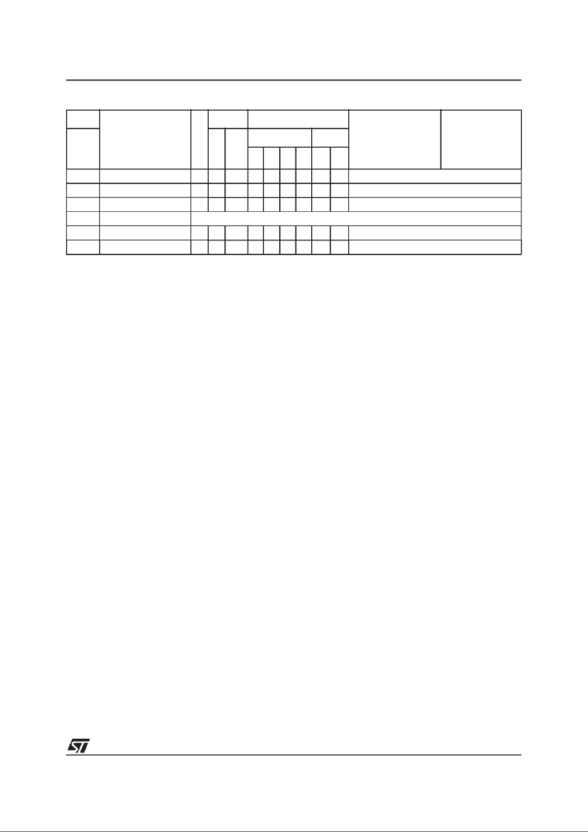
1.3 REGISTER & MEMORY MAP
As shown in Figure 3, the MCU is capable of
adressing 64K bytes of memories and I/O registers.
The available memory locations consist of 64
bytes of register locations, up to 256 bytes of
RAM, 16 bytes of LCD RAM and 4Kbytes of user
program memory. The RAM space includes up to
64 bytes for the stack from 0100h to 013Fh.
The highest address bytes contain the user reset
and interrupt vectors.
Figure 3. Memory Map
0000h
RAM
Program Memory
(4K = 4096 Bytes)
Interrupt & Reset Vectors
HW Registers
014Fh
0040h
003Fh
0150h
EFFFh
Reserved
(see Table 2)
F000h
FFDFh
FFE0h
FFFFh
(see Table 4)
0140h
LCD RAM (16 Bytes)
013Fh
Short Addressing
RAM (zero page)
Stack
(64 Bytes)
0100h
013Fh
0040h
00FFh
(256 Bytes)
ST72411R
9/71
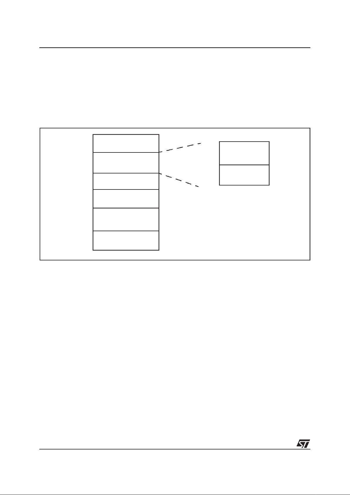
Table 2. Hardware Register Map
Address Block
Register
Label
Register Name
Reset
Status
Remarks
0000h
0001h
0002h
Port A
PADR
PADDR
PAOR
Port A Data Register
Port A Data Direction Register
Port A Option Register
00h
00h
00h
R/W
R/W
R/W
0003h Reserved Area (1 Byte)
0004h
0005h
0006h
Port B
PBDR
PBDDR
PBOR
Port B Data Register
Port B Data Direction Register
Port B Option Register
00h
00h
00h
R/W
R/W
R/W
0007h
to
001Fh
Reserved Area (25 Bytes)
0020h MISCR Miscellaneous Register x0h R/W
0021h
0022h
0023h
Reserved Area (3 Bytes)
0024h LCD LCDCR LCD Control Register 00h R/W
0025h SSS SSSCR
Smartcard Supply Supervisor Control Status
Register
00h R/W
0026h
to
0030h
Reserved Area (11 Bytes)
0031h
0032h
0033h
TIMER
PSCR
TCR
TSCR
Timer Prescaler register
Timer Counter Register
Timer Status Register
FFh
FFh
50h
Read Only
R/W
R/W
0034h
to
003Fh
Reserved Area (12 Bytes)
ST72411R
10/71
1.4 FLASH PROGRAM MEMORY
1.4.1 Introduction
Flash devices have a single voltage non-volatile
FLASH memory that may be programmed in-situ
(or plugged in a programming tool) on a byte-bybyte basis.
1.4.2 Main features
■ Remote In-Situ Programming (ISP) mode
■ Up to 16 bytes programmedin the same cycle
■ MTP memory (Multiple Time Programmable)
■ Read-out memory protection against piracy
1.4.3 Structural organisation
The FLASH program memory is organised in a
single 8-bit wide memory block which can be used
for storing both code and data constants.
The FLASH program memory is mappedin the upper part of the ST7 addressing space (F000hFFFFh) and includes the reset and interrupt user
vector area.
1.4.4 In-Situ Programming (ISP) modes
The FLASH program memory canbe programmed
using two Remote ISP modes. These ISP modes
allow the contents of the ST7 program memory to
be updated using a standard ST7 programming
tool after the device is mounted on the application
board. This feature can be implemented with a
minimum numberof addedcomponents and board
area impact.
Examples of Remote ISP hardware interfaces to
the standard ST7 programming tool are described
below. For more details on ISP programming,refer
to the ST7 Programming Specification.
Remote ISP Overview
The Remote ISP modes are initiated by a specific
sequence on the dedicated ISPSEL pin.
The Remote ISP is performedin three steps:
– Selection of the RAM execution mode
– Download of Remote ISP code in RAM
– Execution ofRemote ISP code in RAM to pro-
gram the user program into the FLASH
Remote ISP hardware configuration
Remote ISP mode works using either the internal
oscillator (no external clock is necessary), or an
external square wave clock. The selection of the
oscillator (internal or external) depends on the
ISP_SEL pin during the rising edge of RESET pin
(see “MAIN CLOCK CONTROLLER SYSTEM
(MCC)” on page 21).
Two ISP modes exist:
■ ISP1: ISP signals mapped onsmartcard I/O pins
■ ISP2: ISP signal mapped on general purpose
I/O pins
ISP1 Mode
In ISP1 mode, it is possible to re-program the microcontroller using a ISO7816 smartcard connector as shown in Figure 3.
This mode requires five signals (plus the SC_PWR
signal if necessary) to be connected to the programming tool. These signals are:
– RESET: device reset
–VSS: device ground power supply
– ISPCLK1: ISP output serial clock pin
– ISPDATA1: ISP input serial data pin
– ISPSEL: Remote ISP modeselection. Thispin
has an internal pulldown and mustbe left high
impedance if the internal oscillator is selected.
Otherwise an appropriate pull-up is needed
(see Electrical Characteristics).
Note: The RESET and ISPSEL pins are not part of
the ISO7816 interface. Consequently, two additional contacts on the smartcard connector are
necessary.
Table 3. ISP1 (Smartcard) interface
ISPSEL
V
SS
RESET
ISPCLK1
ISPDATA1
ST72411
SMARTCARD
FOR ISP
SMARTCARD
CONNECTOR
SC_PWR
V
DD
ISO7816
ST72411R
11/71
FLASH PROGRAM MEMORY (Cont’d)
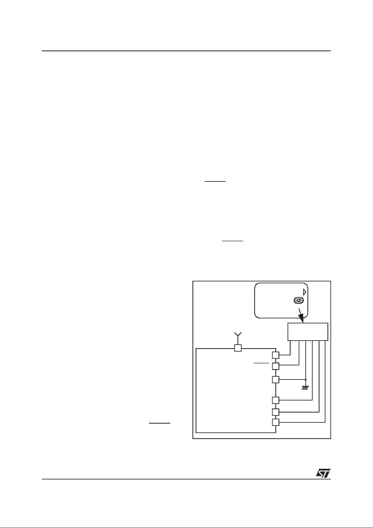
ISP2 Mode
This mode requires five signals (plus the VDDsignal if necessary) to be connected to the programming tool. These signals are:
– RESET: device reset
–VSS: device groundpower supply
– ISPCLK2: ISP output serial clock pin
– ISPDATA2: ISP input serial data pin
– ISPSEL: Remote ISP mode selection. Thispin
must be left high impedance (internal pull
down on pin ISPSEL) if the internal oscillator
is selected. Otherwise an appropriate pull-up
is needed (see Electrical Characteristics).
If anyof these pins are used for other purposes on
the application, a serial resistor has to be implemented toavoid a conflict if the otherdevice forces
the signal level.
Figure 4 shows a typical hardware interface to a
standard ST7 programming tool. For more details
on the pin locations, refer to the device pinout description.
Figure 4. Typical Remote ISP2 Interface
1.5 Program Memory Read-out Protection
The read-out protection is enabled through an option bit.
For FLASH devices, when this option is selected,
the program and data stored in the FLASH memory are protected against read-out piracy (including
a re-write protection). When this protection option
is removed the entire FLASH program memory is
automatically erased.
ISPSEL
V
SS
RESET
ISPCLK2
ISPDATA2
V
DD
ST7
HE10 CONNECTOR TYPE
TO PROGRAMMING TOOL
APPLICATION
4.7kΩ
1
ST72411R
12/71
2 CENTRAL PROCESSING UNIT
2.1 INTRODUCTION
This CPU has a full 8-bit architecture and contains
six internal registers allowing efficient 8-bit data
manipulation.
2.2 MAIN FEATURES
■ 63 basic instructions
■ Fast 8-bit by 8-bit multiply
■ 17 main addressing modes
■ Two 8-bit index registers
■ 16-bit stack pointer
■ Low power modes
■ Maskable hardware interrupts
■ Non-maskable software interrupt
2.3 CPU REGISTERS
The 6 CPU registers shown in Figure 13 are not
present in the memory mapping andare accessed
by specific instructions.
Accumulator (A)
The Accumulator is an 8-bit general purpose register used to hold operands and the results of the
arithmetic and logic calculations and to manipulate
data.
Index Registers (X and Y)
In indexed addressing modes, these 8-bit registers
are used to create either effective addresses or
temporary storage areas for data manipulation.
(The Cross-Assembler generates a precede instruction (PRE) to indicate that the following instruction refers to the Y register.)
The Y registeris not affected by the interrupt automatic procedures (notpushed to and popped from
the stack).
Program Counter (PC)
The program counter is a 16-bit register containing
the address of the next instruction to be executed
by the CPU. It is made of two 8-bit registers PCL
(Program Counter Low which is the LSB) and PCH
(Program CounterHigh which is the MSB).
Figure 5. CPU Registers
ACCUMULATOR
X INDEX REGISTER
Y INDEX REGISTER
STACK POINTER
CONDITION CODE REGISTER
PROGRAM COUNTER
70
1C11HI NZ
RESET VALUE = RESET VECTOR @ FFFEh-FFFFh
70
70
70
0
7
15 8
PCH
PCL
15
87 0
RESET VALUE = STACKHIGHER ADDRESS
RESET VALUE =
1X11X1XX
RESET VALUE = XXh
RESET VALUE = XXh
RESET VALUE = XXh
X = Undefined Value

ST72411R
13/71
CPU REGISTERS (Cont’d)
CONDITION CODE REGISTER (CC)
Read/Write
Reset Value: 111x1xxx
The 8-bit Condition Code register contains the interrupt mask and four flags representative of the
result ofthe instruction just executed. Thisregister
can also be handled by the PUSH and POP instructions.
These bits can be individually tested and/or controlled by specific instructions.
Bit 4 = H
Half carry
.
This bit is set by hardware whena carry occurs between bits 3 and 4 of the ALU during an ADD or
ADC instruction. It is reset by hardware during the
same instructions.
0: No half carry has occurred.
1: A half carry has occurred.
This bit is tested using the JRH or JRNH instruction. The H bit is useful in BCD arithmetic subroutines.
Bit 3 = I
Interrupt mask
.
This bit is set by hardware when entering in interrupt or by software to disable all interrupts except
the TRAP software interrupt. This bit is cleared by
software.
0: Interrupts are enabled.
1: Interrupts are disabled.
This bit is controlledby the RIM, SIM and IRET instructions and is tested by the JRM and JRNM instructions.
Note: Interrupts requested while I is set are
latched and can be processed when I is cleared.
By default an interrupt routine is not interruptable
because the I bit is set by hardware when you en-
ter it and reset by the IRET instruction at the end of
the interrupt routine. If the I bit is cleared by software in the interrupt routine, pending interrupts are
serviced regardless of the priority level of the current interrupt routine.
Bit 2 = N
Negative
.
This bit is set and cleared by hardware. It is representative of the result sign of the last arithmetic,
logical or data manipulation. It is a copy of the 7
th
bit of the result.
0:Theresultof the lastoperationis positive or null.
1: The result of the last operation is negative
(i.e. the most significant bit is a logic 1).
This bit isaccessed by the JRMI andJRPL instructions.
Bit 1 = Z
Zero
.
This bit is set and cleared by hardware. This bit indicates thatthe result of the last arithmetic, logical
or data manipulation is zero.
0: The result of the last operation is different from
zero.
1: The result of the last operation is zero.
This bit is accessed by the JREQ and JRNE test
instructions.
Bit 0 = C
Carry/borrow.
This bit is set and cleared by hardware and software. It indicates an overflow or an underflow has
occurred during the last arithmetic operation.
0: No overflow or underflow has occurred.
1: An overflow or underflow hasoccurred.
This bit is driven by the SCF and RCF instructions
and tested by the JRC and JRNC instructions. It is
also affected by the “bit test and branch”, shift and
rotate instructions.
70
111HINZC
ST72411R
14/71
CENTRAL PROCESSING UNIT (Cont’d)
STACK POINTER (SP)
Read/Write
Reset Value: 013Fh
The Stack Pointer is a 16-bit register which is always pointingto the next free location in the stack.
It isthen decremented after data has been pushed
onto the stack and incremented before data is
popped from the stack (see Figure 6).
Since the stack is 64 bytes deep, the 10 most significant bits are forced by hardware. Following an
MCU Reset, orafter a Reset Stack Pointer instruction (RSP),the Stack Pointer contains its resetvalue (the SP5 to SP0 bitsare set) whichis the stack
higher address.
The least significant byte of the Stack Pointer
(called S) can be directly accessed by a LD instruction.
Note: When the lower limit is exceeded, the Stack
Pointer wraps around to the stackupper limit, without indicating the stack overflow. The previously
stored information is then overwritten and therefore lost. The stack also wrapsin caseof anunderflow.
The stack is used to save the return address during a subroutine call and the CPU context during
an interrupt. The user may also directly manipulate
the stack by meansof the PUSH and POP instructions. In the case of an interrupt, the PCL is stored
at the first location pointed to by the SP. Then the
other registers are stored in the next locations as
shown in Figure 6.
– When an interrupt is received, the SP is decre-
mented and the context is pushed on the stack.
– On return from interrupt, the SP is incremented
and the context is popped from thestack.
A subroutine call occupies twolocations and an interrupt five locations in the stack area.
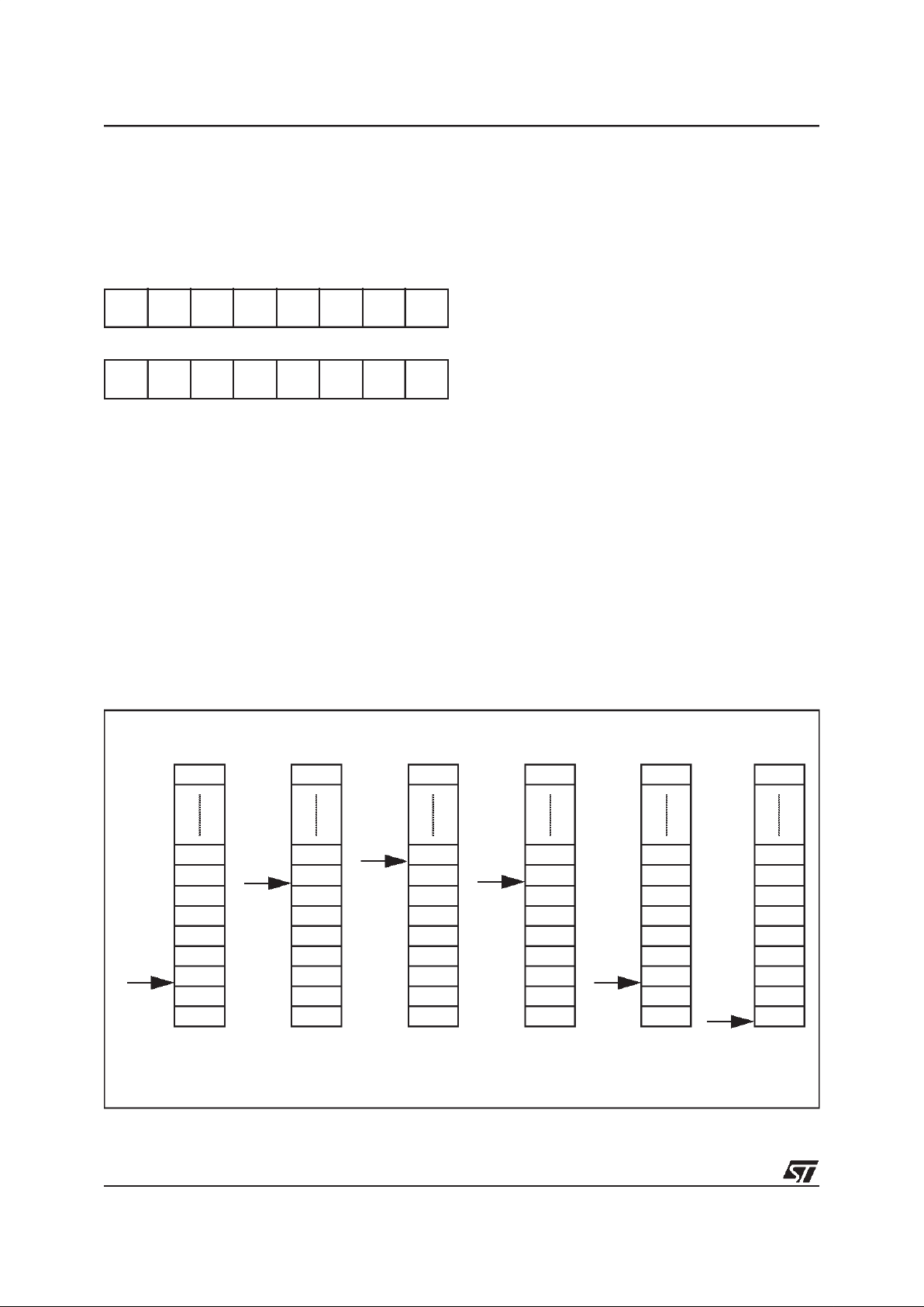
Figure 6. Stack Manipulation Example
15 8
00000001
70
0 0 SP5 SP4 SP3 SP2 SP1 SP0
PCH
PCL
SP
PCH
PCL
SP
PCL
PCH
X
A
CC
PCH
PCL
SP
PCL
PCH
X
A
CC
PCH
PCL
SP
PCL
PCH
X
A
CC
PCH
PCL
SP
SP
Y
CALL
Subroutine
Interrupt
Event
PUSH Y POP Y IRET
RET
or RSP
@ 013Fh
@ 0100h
Stack Higher Address = 013Fh
Stack Lower Address =
0100h

ST72411R
15/71
3 SUPPLY, RESET AND CLOCK MANAGEMENT
The ST72411 microcontroller includes a range of
utility features for securing the application in critical situations (for example in case of a power
brown-out), and reducing the number of external
components.
Main Features
■ V
DD
Low Voltage Detection and Supervisor
(LVDS)
■ Reset Sequence Manager
■ Main Clock Controller System (MCC)
3.1 LOW VOLTAGE DETECTOR AND
SUPERVISOR (LVDS)
The LVDS consists of three main blocks:
– Low Voltage Detector (LVD)
– Open Power Supply Detection (OPSD)
– Power Supply Supervisor (PSS)
If the internal oscillator is selected (OSC_SEL pin
is tied to VSS), the LVDS, OPSD and PSS functions are always enabled.
If an external clock is selected (OSC_SEL tied to
VDD), the LVDS, OPSD and PSS are disabled
while the external RESET is low and during the
first 260 clock cycles (f
CPU
). They become enabled after this period. Refer to Figure 13. This
means an external reset circuit must be provided.
However, afterthis periodthe LVDS may generate
a reset if a power voltage drop occurs.
3.1.1 Low Voltage Detector
To allow the integration of power management
features in the application, the Low Voltage Detector function (LVD) generates a static reset when
the VDDsupply voltage is below a V
IT+
reference
value (positive-going input thresholdvoltage). This
means that it secures the power-up as well as the
power-down by keeping the ST7 in reset state.
The V
IT-
reference value (negative-going input
threshold voltage) for a voltage drop is lower than
the V
IT+
reference value for power-on in order to
avoid a parasitic reset when the MCU starts running and sinks current on the supply(hysteresis).
The LVD Reset circuitry generates a reset when
VDDis below:
–V
IT+
when VDDis rising
–V
IT-
when VDDis falling
The LVD function is illustrated in Figure 7.
Provided the minimum VDDvalue (guaranteed for
the oscillator frequency) is below V
IT-
, the MCU
can only be in one of two modes:
– Under full software control
– In static safe reset
In this condition, secure operation is always ensured for the application without the need for external reset hardware.
The LVD filters spikes on VDDlarger than t
g(VDD)
to
avoid parasitic resets.
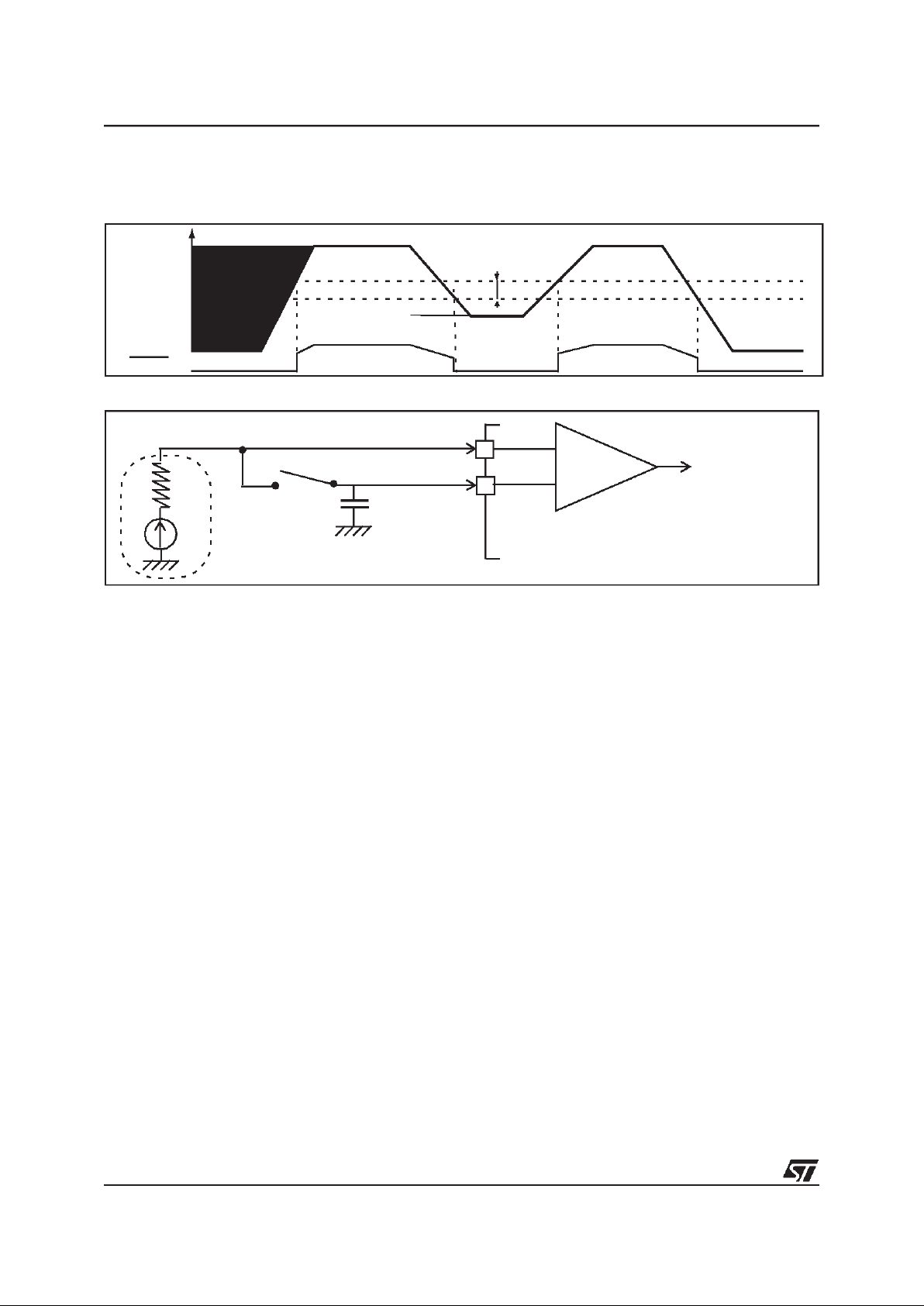
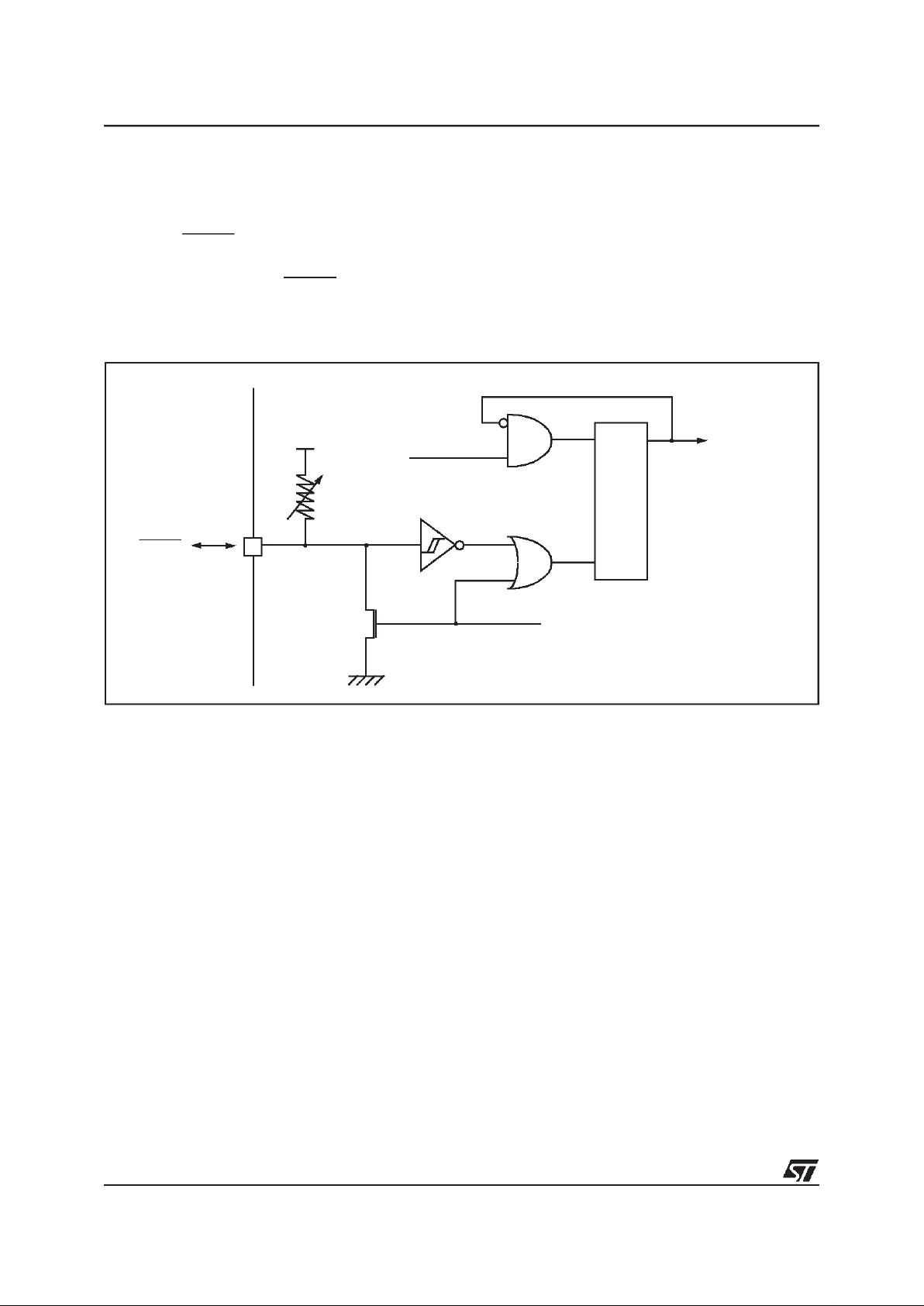
3.1.2 Open Power Supply Detection (OPSD)
The purpose of the Open Power Supply Detection
function is to detect if the VDDpower circuit is
open.
It detects if the microcontroller is about to be powered down, to allow software to shutdown the application properly before the Power Down Reset
generate by the LVDS.
The system is based on a comparison between
V
REF
andVDD.V
REF
is an analog input which is intended to be directly connected to the power
source (see Figure 8).
The detection is not dependent on the MCU consumption (not dependent on the voltage drop due
to the internal resistor of the power source).
To avoid spurious setting of the Power Down Flag
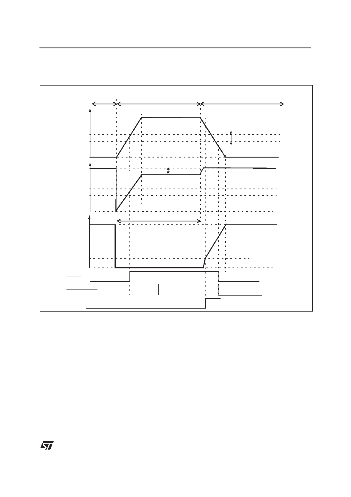
due to possible noise (PDF bit in the MISCR register), a margin M is factored into the comparison.
The detectionis done if:
(V
REF-VDD
)>M
The PDF flag can be used to monitor the main
supply supervisor function as shown in Figure 9.
When (V
REF-VDD
) > M, the PDFflag is set and an
interrupt is generated if the PDIE bit in the MISCR
register is set. This feature allows the user program to detect and manage the VDDdrop according to the application before the reset generated
by the LVDS (See Figure 9).
See the Miscellaneous register chapter for more
details on the PDF and PDIE bits.
3.1.3 Power Supply Supervisor (PSS)
The Power Supply Supervisor function compares
the Power Supply to a fixed analog reference voltage (V
PSS
) (see Figure 10). The output of this
comparator is directly connected to the PSSF bitin
the MISCR register (read only bit).
This feature can be used to monitor the power
supply.
ST72411R
16/71
LOW VOLTAGE DETECTOR AND SUPERVISOR (Cont’d)
Figure 7. Low Voltage Detector vs Reset
Figure 8. Open Power Supply Detection: V
REF
Connections
V
DD
V
IT+
RESET
V
IT-
HYSTERESIS
V
hys
V
DD
V
REF
R
S
Power
V
E
+
-
C
Power Down Flag
Source
(PDF)generation
SW1
if (V
REF-VDD
)>M
ST72411R
17/71
LOW VOLTAGE DETECTOR AND SUPERVISOR (Cont’d)
Figure 9. Open Power Supply Detection (OPSD)
Figure 10. Power Supply Supervisor system (PSS)
V
’’
RESET
V
IT+
V
IT-
HYSTERESIS
V
hys
PDF
Internal RESET
RUN
Open V
DD
detection
V
5()
V
5()
V
’’
DV = RS.I
RUN
V
E
V
DDRUN
V
DDRUN
0V
+V
E
RESET
SW1 OPEN SW1 CLOSED SW1 OPEN
0V
0V
V
5( )
V
’’
M
(CAPACITOR
DISCHARGED)
ST72411R
18/71
3.2 RESET SEQUENCE MANAGER
The RESET sequence manager includes two reset sources as shown in Figure 11:
■ External RESET source pulse
■ Internal LVDS RESET (Low Voltage Detection)
These sources act on the RESET PIN and it is always kept low during the delay phase.
The RESET service routine vector is fixed at addresses FFFEh-FFFFh in the ST7 memory map.
A 4096 CPUclock cycle delay allows the oscillator
to stabilise and to ensure that recovery has taken
place from the Reset state.
The RESET vector fetch phase duration is 2 clock
cycles.
Figure 11. Reset Block Diagram
f
CPU
COUNTER
RESET
R
ON
V
DD
LVD RESET
INTERNAL
RESET
ST72411R
19/71
RESET MANAGER (Cont’d)
([WHUQD O 5(6( 7 SLQ
The RESETpin is both an input andan open-drain
output with integrated RONweak pull-up resistor
(see Figure11). This pull-up has nofixed value but
varies in accordance with the input voltage. It can
be pulled low by external circuitry to reset the device.
A RESET signal coming from an external source
must have a duration of at least t
PULSE
in order to
be recognized. Two RESET sequences can be associated with this RESET source as shown in Figure 12.
When the RESET is generated by an internal
source, during the two first phases of the RESET
sequence, the device RESET pin acts as an output that is pulled low.
Figure 12. External RESET Sequence with internal Clock Selected (OSC_SEL pin tied to VSS)
Figure 13. External RESET Sequence with External Clock Selected (OSC_SEL pin tied to VDD)
5(6(7
581
INTERNAL RESET
4096 CLOCK CYCLES
FETCH
VECTOR
581
t
PULSE
9
’’
V
IT+
V
DD nominal
DELAY
RESET PIN
EXTERNAL
RESET SOURCE
5(6(7
581
INTERNAL RESET
260 CLOCK
FETCH
VECTOR
581
t
PULSE
9
’’
V
IT+
V
DD nominal
DELAY
LVDS,
ONOFF
OPSD,
PSS
4096 CLOCK CYCLES
CYCLES
ON
RESET PIN
EXTERNAL
RESET SOURCE
ST72411R
20/71
RESET MANAGER (Cont’d)
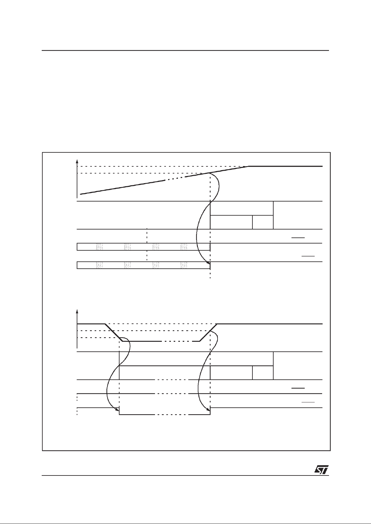
,QWHUQD O /RZ 9ROWDJ H ’HWHFWL RQ 5 ( 6 ( 7
Two different RESET sequences caused bythe internal LVD circuitry can be distinguished:
- LVD Power-On RESET
- Voltage Drop RESET
In the second sequence, a “delay” phase is used
to keep the device in RESET state until VDDrises
up to V
IT+
(see Figure 14).
Important: if OSC_SEL pin is HIGH (external
clock selected), the LVD Power-On and the Voltage Drop featuresare disabled during the first 260
clock cycles (f
CPU
) after reset. This means that an
external reset circuitry must be provided to reset
the microcontroller.
Figure 14. LVD RESET Sequences when the OSC_SEL pin is tied to GND
5( 6( 7
581
INTERNAL RESET
4096 CLOCK CYCLES
FETCH
VECTOR
32 : ( 5
RESET PIN
EXTERNAL RESET SOURCE
5(6(7
581
INTERNAL RESET
4096 CLOCK CYCLES
FETCH
VECTOR
581
RESET PIN
EXTERNAL RESET SOURCE
9
’’
V
DDnominal
DELAY
V
IT+
V
IT-
9
’’
V
DDnominal
V
IT+
/
9
’
3
2
:
(
5
2
1
5
(
6
(
7
9
2
/
7
$
*
(
’
5
2
3
5
(
6
(
7
2))
7KH 2 6 &B6( / SLQ LV WLHG WR 9
66
LQWHU QD O FORFN VHOHFWHG / 9 ’ 6 D OZD\V DFWLYDWHG
7KH 2 6&B6( / SLQ LV WLHG WR * 1 ’
LQWHU QDO FORFN
V
HOHFWHG / 9 ’ 6 DOZD\V DFWLYDWHG
ST72411R
21/71
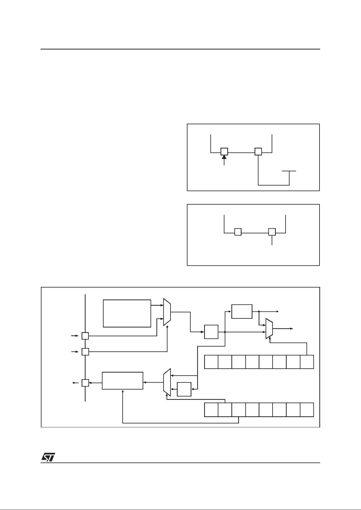
3.3 MAIN CLOCK CONTROLLER SYSTEM (MCC)
The MCC block supplies the clock for the ST7
CPU and its internal peripherals. It allows to manage the SLOW power saving mode acting on the
SMS bit of the Miscellaneous register (MISCR)
and the Main clock-out capability acting on the
CKD and CKAFOEN bits of the Smartcard Supply
Supervisor ControlRegister (SSSCR).
The main clock of the ST7 can be generated by
two different sources (see Figure 17):
■ an external source
■ an internal RC oscillator
The device is normally operated using anintegrated 7.16MHz oscillator, meaning 3.58MHz operating frequency. However, an external clock can be
applied, up to 8MHz (4MHz operating frequency).
The clock source is selected through the
OSC_SEL pin status.
([WHUQD O &ORFN 6RXUFH
The OSC_SEL pin status selects the External
Clock capability when it is tied to VDD. In this
mode, a clock signal with ~50% duty cycle has to
drive the OSCIN pin (see Figure 15).
,QWHUQD O 5& 2VFLOODWRU 6RXUFH
The OSC_SEL pin status selects the Internal RC
clock source capability when it is tied to VSS(see
Figure 16).
Note that OSC_SEL pin contains a pull-down
which allows to leave OSC_SEL in high impedance in the applicationwhen the internal oscillator
is selected. This is mandatory for using the Remote In Situ Programming feature.
Figure 15. External Clock
Figure 16. Internal RC Oscillator
Figure 17. Main Clock Controller (MCC) Block Diagram
OSCIN OSC_SEL
EXTERNAL
ST7
SOURCE
V
DD
OSCIN OSC_SEL
ST7
highZ
(internal pulldown is present)
DIV 2
SMS--
MISCR
f
OSC
f
CPU
OSCIN
-----
INTERNAL
RC OSCILLATOR
7.16 MHz
OSC_SEL
DIV 16
SMARTCARD
interface
LCD and TIMER
---
SSSR
CK_A
--CKD-
FOEN
DIV 2
I/O ALTERNATE
FUNCTION
SC_CK

ST72411R
22/71
4 INTERRUPTS
The ST7 core may be interruptedby one of two different methods: maskable hardware interrupts as
listed in the Interrupt Mapping Table and a nonmaskable software interrupt (TRAP). The Interrupt
processing flowchart is shown in Figure 1.
The maskableinterrupts must be enabled clearing
the I bit in order to be serviced. However, disabled
interrupts may be latched and processed when
they are enabled (see external interrupts subsection).
When an interrupt has to be serviced:
– Normal processing is suspended at the end of
the current instruction execution.
– The PC, X, A and CC registers are saved onto
the stack.
– The I bit of the CC register is set to prevent addi-
tional interrupts.
– ThePC is then loaded withtheinterrupt vector of
the interruptto service and the first instruction of
the interrupt service routine is fetched (refer to
the Interrupt Mapping Table for vector addresses).
The interrupt service routine should finish with the
IRET instruction which causes the contents of the
saved registers to be recovered from thestack.
Note: As a consequence of the IRET instruction,
the I bit will be cleared and the main program will
resume.
Priority management
By default, a servicing interrupt cannot be interrupted because the I bit is set by hardware entering in interrupt routine.
In the case when several interrupts are simultaneously pending, an hardware priority defines which
one will be serviced first (see the Interrupt Mapping Table).
Interrupts and Low power mode
All interrupts allow the processor to leave the
WAIT low power mode. Only external and specifically mentioned interrupts allow the processor to
leave the HALT low power mode (refer to the “Exit
from HALT“ column in the Interrupt Mapping Table).
4.1 NON MASKABLE SOFTWARE INTERRUPT
This interrupt is entered when the TRAP instruction is executed regardless of the state of the I bit.
It will be serviced according to the flowchart on
Figure 1.
4.2 EXTERNAL INTERRUPTS
External interrupt vectors can be loaded into the
PC register if the corresponding external interrupt
occurred and if the I bit is cleared.These interrupts
allow the processor to leave the Halt low power
mode.
The external interrupt polarity is selected through
the miscellaneous register or interrupt register (if
available).
An external interrupt triggered on edge will be
latched and the interrupt request automatically
cleared upon entering the interrupt serviceroutine.
If several input pins, connected to the same interrupt vector, are configured as interrupts, their signals are logically ANDed before entering the edge/
level detection block.
Caution:The type of sensitivity defined inthe Miscellaneous or Interrupt register (if available) applies to the ei source. In case of an ANDedsource
(as described on the I/O ports section), a lowlevel
on an I/O pin configured as input with interrupt,
masks the interrupt requesteven in case of risingedge sensitivity.
4.3 PERIPHERAL INTERRUPTS
Different peripheral interrupt flags in the status
register are able to cause an interrupt when they
are active if both:
– The I bit of the CC register is cleared.
– Thecorrespondingenablebit isset in the control
register.
If any of these two conditions is false, the interrupt
is latched and thus remains pending.
Clearing an interrupt request is done by:
– Writing “0”to the corresponding bit in the status
register or
– Access tothe status registerwhile the flag is set
followed by a read or write of an associated register.
Note: the clearing sequence resets the internal
latch. A pending interrupt (i.e. waiting for being enabled) will therefore be lost ifthe clear sequence is
executed.
 Loading...