

SGS Thomson Microelectronics ST72C124J2, ST72C334N4, ST72C334N2, ST72C334J4, ST72C334J2 Datasheet
...
Rev. 2.1
May 2000 1/148
This ispreliminary information on anew product in development or undergoing evaluation. Details are subject tochange without notice.
ST72334J/N,
ST72314J/N, ST72124J
8-BIT MCU WITH SINGLE VOLTAGE FLASH MEMORY,
ADC, 16-BIT TIMERS, SPI, SCI INTERFACES
PRELIMINARY DATA
■ Memories
– 8K or 16K Program memory (ROM or single
voltage FLASH) with read-out protection and
in-situ programming (remote ISP)
– 256 bytes EEPROM Data memory (with read-
out protection option in ROM devices)
– 384 or 512 bytes RAM
■ Clock, Reset and Supply Management
– Enhanced reset system
– Enhanced low voltage supply supervisor with
3 programmable levels
– Clock sources: crystal/ceramic resonator os-
cillators or RC oscillators, external clock,
backup Clock Security System
– 4 Power Saving Modes: Halt, Active-Halt,
Wait and Slow
– Beep and clock-out capabilities
■ Interrupt Management
– 10 interrupt vectors plus TRAP and RESET
– 15 external interrupt lines (4 vectors)
■ 44 or 32 I/O Ports
– 44 or 32 multifunctionalbidirectional I/O lines:
– 21 or 19 alternate function lines
– 12 or 8 high sink outputs
■ 4 Timers
– Configurable watchdog timer
– Realtime base
– Two 16-bit timers with: 2 input captures (only
one on timer A), 2 output compares (only one
on timer A), External clock input on timer A,
PWM and Pulse generator modes
■ 2 Communications Interfaces
– SPI synchronous serial interface
– SCI asynchronous serial interface
■ 1 Analog Peripheral
– 8-bit ADC with 8 input channels (6 only on
ST72334Jx, not available on ST72124J2)
■ InstructionSet
– 8-bit data manipulation
– 63 basic instructions
– 17 main addressing modes
– 8 x 8 unsigned multiply instruction
– True bit manipulation
■ Development Tools
– Full hardware/softwaredevelopment package
Device Summary
TQFP44
10x10
PSDIP42
PSDIP56
TQFP64
14 x 14
Features ST72124J2 ST72314J2 ST72314J4 ST72314N2 ST72314N4 ST72334J2 ST72334J4 ST72334N2 ST72334N4
Program memory - bytes 8K 8K 16K 8K 16K 8K 16K 8K 16K
RAM (stack) - bytes 384 (256) 384 (256) 512 (256) 384 (256) 512 (256) 384 (256) 512 (256) 384 (256) 512 (256)
EEPROM - bytes - - - --256 256 256 256
Peripherals
Watchdog, Two 16-bit Timers, SPI, SCI
-ADC
Operating Supply 3.0V to 5.5V
CPU Frequency Up to 8 MHz (with up to 16 MHz oscillator)
Operating Temperature -40°C to +85°C (-40°C to +105/125°Coptional)
Packages TQFP44 / SDIP42 TQFP64 /SDIP56 TQFP44 /SDIP42 TQFP64 /SDIP56
1

Table of Contents
148
2/148
2
1 PREAMBLE: ST72C334 VERSUS ST72E331 SPECIFICATION . . . . . . . . . . . . . ............ 4
2 INTRODUCTION . . . . . . . . . . . . . . . . . . . . . ......................................... 5
3 PIN DESCRIPTION . . . . . . . . . . . . ................................................ 6
4 REGISTER & MEMORY MAP . . . ................................................ 12
5 FLASH PROGRAM MEMORY . . . . . . . . . . . . . . . . . ................................. 16
5.1 INTRODUCTION . ...................................................... 16
5.2 MAIN FEATURES . . . . . . . . . . . . . . . . . . . . . . . . . . . . . . . .. . .................... 16
5.3 STRUCTURAL ORGANISATION . . . . . . . . . . . . . . . ........................... 16
5.4 IN-SITU PROGRAMMING (ISP) MODE . .................................... 16
5.5 MEMORY READ-OUT PROTECTION . . . . . ................................. 16
6 DATA EEPROM . . . . . . . . . .................................................... 17
6.1 INTRODUCTION . ...................................................... 17
6.2 MAIN FEATURES . . . . . . . . . . . . . . . . . . . . . . . . . . . . . . . .. . .................... 17
6.3 MEMORY ACCESS . . . . . . . . . . . . . . . . . . . . . . . . . . . .. . . . . . . . . . . . . . . . . ........ 18
6.4 POWER SAVING MODES . . . . . . ......................................... 19
6.5 ACCESS ERROR HANDLING . . . . . . . . . . . ................................. 19
6.6 REGISTER DESCRIPTION . . . . . . . .. . . . . . . . . . . . . . . . . . . . . . . . . . . . . . . ........ 20
6.7 READ-OUT PROTECTION OPTION . . . . . . . . . . . . . . . . . . . . . . . . . . . . . . . . ........ 20
7 CENTRAL PROCESSING UNIT . . ............................................... 21
7.1 INTRODUCTION . ...................................................... 21
7.2 MAIN FEATURES . . . . . . . . . . . . . . . . . . . . . . . . . . . . . . . .. . .................... 21
7.3 CPU REGISTERS . . .. . . . . . . . . . . . . . . . . . ................................. 21
8 SUPPLY, RESET AND CLOCK MANAGEMENT . . . . ................................24
8.1 LOW VOLTAGE DETECTOR (LVD) . . . . . . . .................................25
8.2 RESET SEQUENCE MANAGER (RSM) . . . . ................................. 26
8.3 MULTI-OSCILLATOR (MO) . . . . . . . . . . . . . . . ................................ 28
8.4 CLOCK SECURITY SYSTEM (CSS) . . . . . . . . ................................29
8.5 SUPPLY, RESET AND CLOCK REGISTER DESCRIPTION . .................... 30
9 INTERRUPTS . . ............................................................. 31
9.1 NON MASKABLE SOFTWARE INTERRUPT . . . . . . ........................... 31
9.2 EXTERNAL INTERRUPTS . . . . . . . . . . . . . .................................. 31
9.3 PERIPHERAL INTERRUPTS . . ...........................................31
10 POWER SAVING MODES . . . . . ............................................... 33
10.1 INTRODUCTION . ...................................................... 33
10.2 SLOW MODE . . . . . . . . . . . . . . ...........................................33
10.3 WAIT MODE . . . . . . . . . . . ............................................... 34
10.4 ACTIVE-HALT AND HALT MODES . . . . . . . . . . . . . . . . . . . . . . . . . . . . . . . . . . . . . . . . 35
11 I/O PORTS . . . .............................................................. 37
11.1 INTRODUCTION . ...................................................... 37
11.2 FUNCTIONAL DESCRIPTION . . . . ........................................37
11.3 I/O PORT IMPLEMENTATION . . . . ........................................ 40
11.4 LOW POWER MODES . . . . . . . . . . . . . . . . . ................................. 41

Table of Contents
3/148
3
11.5 INTERRUPTS . . . . . . . . . . . . . . . . . . . . . . . . ................................. 41
12 MISCELLANEOUS REGISTERS . . . . . . . . . . . . . . . . . . . . . . . . . . . . . . . . . . .. . . . . . . . . . . . 44
12.1 I/O PORT INTERRUPT SENSITIVITY . . . . . . ................................44
12.2 I/O PORT ALTERNATE FUNCTIONS . . . . . .................................. 44
12.3 REGISTERS DESCRIPTION . . . . . . . . . .................................... 45
13 ON-CHIP PERIPHERALS . . . . . . ............................................... 47
13.1 WATCHDOG TIMER (WDG) . . . . . . . . . . . . . . . . . . . ........................... 47
13.2 MAIN CLOCK CONTROLLER WITH REAL TIME CLOCK TIMER (MCC/RTC) . .. . . . . 50
13.3 16-BIT TIMER . . . . . . . . . . . . . . . . . . . . . . . . . . . . . . . . . . . . . . . . . . . . . . . . . ........ 52
13.4 SERIAL PERIPHERAL INTERFACE (SPI) . .................................. 70
13.5 SERIAL COMMUNICATIONS INTERFACE (SCI) . . . . . . . . . . . . . . . . . . . . . . . . . . . . . . 83
13.6 8-BIT A/D CONVERTER (ADC) ........................................... 95
14 INSTRUCTION SET . . . . . . . . . . . . . . . . . . . . . . . . ................................. 99
14.1 ST7 ADDRESSING MODES . . . . . . . . . . . . . . . .. . . . . . . . . . . . . . . . . . . . . . . . . . . . . . 99
14.2 INSTRUCTION GROUPS . . . . . . . . . . . . . . . . . . ............................. 102
15 ELECTRICAL CHARACTERISTICS . . . . ........................................ 105
15.1 PARAMETER CONDITIONS . . . . . . . . .. . . . . . . ............................. 105
15.2 ABSOLUTE MAXIMUM RATINGS . . . . . . . . . . . . . . . . . . . . . . . . . . . . . . . . . . . . . . . . 106
15.3 OPERATING CONDITIONS . . . . . . . . . . ................................... 107
15.4 SUPPLY CURRENT CHARACTERISTICS . . . ...............................110
15.5 CLOCK AND TIMING CHARACTERISTICS . . . . . . . . . . . . . . . . . . . . . . . .......... 113
15.6 MEMORY CHARACTERISTICS . . . ....................................... 119
15.7 EMC CHARACTERISTICS . . . . . . . . . . . . . . . . . . . . . . . . . . . . . . . . . . . . . . . . . .. . . . 120
15.8 I/O PORT PIN CHARACTERISTICS .......................................125
15.9 CONTROL PIN CHARACTERISTICS . . . . . ................................. 128
15.10 TIMER PERIPHERAL CHARACTERISTICS . . . . . . . . . . . . . . . . . . . . . . . . . . ....... 131
15.11 COMMUNICATION INTERFACE CHARACTERISTICS . . . . . ................... 132
15.12 8-BIT ADC CHARACTERISTICS . . . . . . . . ................................. 135
16 PACKAGE CHARACTERISTICS . . . . . . ........................................ 137
16.1 PACKAGE MECHANICAL DATA . . . . . . . . . . . . ............................. 137
16.2 THERMAL CHARACTERISTICS . . . . . . . . . . . . . . . . . . . .. . ................... 139
16.3 SOLDERING AND GLUEABILITY INFORMATION . . . .. . . . . . . . . . . . . . . . . ....... 140
16.4 PACKAGE/SOCKET FOOTPRINT PROPOSAL . . . . . . . . . . . ................... 141
17 DEVICE CONFIGURATION AND ORDERING INFORMATION . . . . . . . . . . . . . . . . . . . . . . . 143
17.1 OPTION BYTES . . . ................................................... 143
17.2 DEVELOPMENT TOOLS . . . . . . . . . . . . . . . . . . . . . .......................... 146
18 SUMMARY OF CHANGES . .................................................. 147

ST72334J/N, ST72314J/N, ST72124J
4/148
1 PREAMBLE: ST72C334 VERSUS ST72E331 SPECIFICATION
New Features available on the ST72C334
■ 8 or 16K FLASH/ROM with In-Situ
Programming and Read-out protection
■ New ADC with abetter accuracyand conversion
time
■ New configurable Clock, Reset and Supply
system
■ New power saving mode with real time base:
Active Halt
■ Beep capability on PF1
■ New interrupt source: Clock security system
(CSS) or Main clock controller(MCC)
ST72C334 I/O Configuration and Pinout
■ Same pinout as ST72E331
■ PA6 and PA7 are true open drain I/O ports
without pull-up (same as ST72E331)
■ PA3, PB3, PB4 and PF2 have no pull-up
configuration (all I/Os present on TQFP44)
■ PA5:4, PC3:2, PE7:4 and PF7:6 have high sink
capabilities (20mA on N-buffer, 2mA on P-buffer
and pull-up). On the ST72E331, all these pads
(except PA5:4) were 2mA push-pull pads
without high sink capabilities. PA4 and PA5
were 20mA true open drains.
New Memory Locations in ST72C334
■ 20h: MISCR register becomes MISCR1 register
(naming change)
■ 29h: new control/status register for the MCC
module
■ 2Bh: new control/status register for the Clock,
Reset and Supply control.This registerreplaces
the WDGSR register keeping the WDOGF flag
compatibility.
■ 40h: new MISCR2 register
ST72334J/N, ST72314J/N, ST72124J
5/148
2 INTRODUCTION
The ST72334J/N,ST72314J/N and ST72124J devices aremembers of the ST7 microcontroller family. They can be grouped as follows:
– ST72334J/Ndevices are designed formid-range
applications with Data EEPROM, ADC, SPI and
SCI interface capabilities.
– ST72314J/N devices target the same range of
applications but without Data EEPROM.
– ST72124J devices are for applications that do
not need Data EEPROM and the ADC peripheral.
All devices are based on a common industrystandard 8-bit core, featuringan enhanced instruction set.
The ST72C334J/N, ST72C314J/N and
ST72C124J versions feature single-voltage
FLASH memory with byte-by-byte In-Situ Programming (ISP) capability.
Under software control, all devices can be placed
in WAIT, SLOW, ACTIVE-HALT or HALT mode,
reducing power consumption when the application
is in idle or standby state.
The enhanced instruction set and addressing
modes of the ST7 offer both power and flexibilityto
software developers, enabling the design ofhighly
efficient andcompact application code. In addition
to standard 8-bit data management, all ST7 microcontrollers feature true bit manipulation, 8x8 unsigned multiplication and indirect addressing
modes.
For easy reference, all parametric data are located
in Section 15 on page 105.
Figure 1. General Block Diagram
8-BIT CORE
ALU
ADDRESS AND DATA BUS
OSC1
ISPSEL
CONTROL
PROGRAM
(8K or 16K Bytes)
V
SS
RESET
PORT F
PF7,6,4,2:0
(6-BIT)
TIMER A
BEEP
PORT A
RAM
(384 or 512 Bytes)
PORT C
8-BIT ADC
V
DDA
V
SSA
PORT B
PB7:0
PORT E
PE7:0
SCI
TIMER B
PA7:0
PORT D
PD7:0
SPI
PC7:0
(8-BIT)
V
DD
EEPROM
(256 Bytes)
WATCHDOG
MULTI OSC
LVD
OSC2
MEMORY
MCC/RTC
+
CLOCK FILTER
(8-BIT for N versions)
(5-BIT for J versions)
(8-BIT for N versions)
(5-BIT for J versions)
(6-BIT for N versions)
(2-BIT for J versions)
(8-BIT for N versions)
(6-BIT for J versions)
ST72334J/N, ST72314J/N, ST72124J
6/148
3 PIN DESCRIPTION
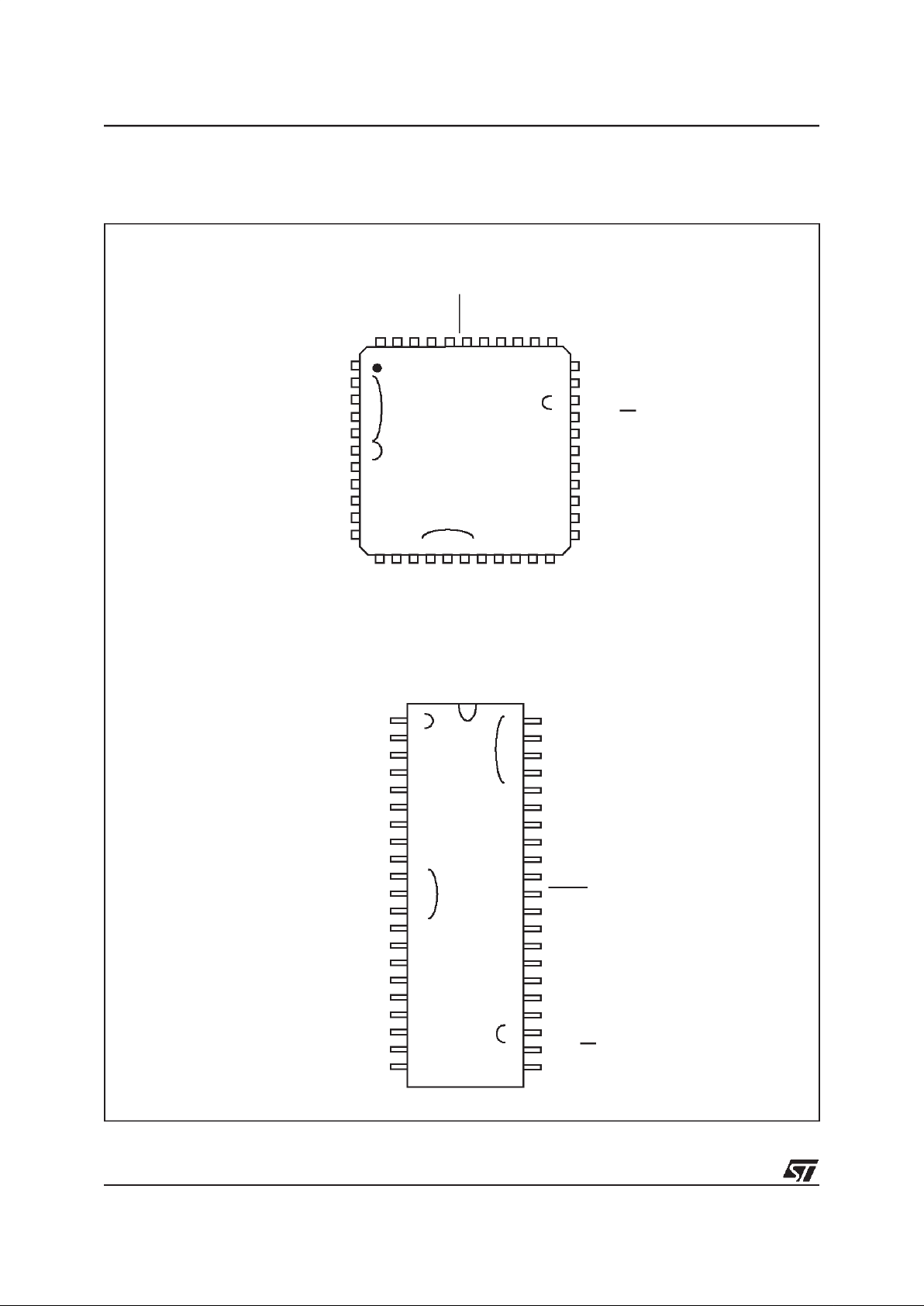
Figure 2. 64-Pin TQFP Package Pinout (N versions)
V
DDA
V
SSA
V
DD_3
V
SS_3
MCO / PF0
BEEP / PF1
PF2
NC
OCMP1_A / PF4
NC
ICAP1_A / (HS) PF6
EXTCLK_A / (HS) PF7
AIN4 / PD4
AIN5 / PD5
AIN6 / PD6
AIN7 / PD7
64 63 62 61 60 59 58 57 56 55 54 53 52 51 50 49
48
47
46
45
44
43
42
41
40
39
38
37
36
35
34
33
17 18 19 20 21 22 23 24 29 30 31 3225 26 27 28
1
2
3
4
5
6
7
8
9
10
11
12
13
14
15
16
ei2
ei3
ei0
ei1
PB0
PB1
PB2
PB3
PB4
PB5
PB6
PB7
AIN0 / PD0
AIN1 / PD1
AIN2 / PD2
AIN3 / PD3
(HS) PE4
(HS) PE5
(HS) PE6
(HS) PE7
PA1
PA0
PC7 / SS
PC6 / SCK / ISPCLK
PC5 / MOSI
PC4 / MISO / ISPDATA
PC3 (HS)/ ICAP1_B
PC2 (HS)/ ICAP2_B
PC1 / OCMP1_B
PC0 / OCMP2_B
V
SS_0
V
DD_0
V
SS_1
V
DD_1
PA3
PA2
V
DD
_2
OSC1
OSC2
V
SS
_2
NCNCRESET
ISPSEL
PA7 (HS)
PA6 (HS)
PA5 (HS)
PA4 (HS)
NCNCPE1 / RDI
PE0 / TDO
(HS) 20mA high sink capability
ei
x
associated external interrupt vector
ST72334J/N, ST72314J/N, ST72124J
7/148
PIN DESCRIPTION (Cont’d)
Figure 3. 56-Pin SDIP Package Pinout (N versions)
52
51
50
49
48
47
46
45
44
43
42
41
16
15
1
2
3
4
5
6
7
8
9
10
11
12
13
14
53
54
55
56
PB4
PB5
BEEP / PF1
MCO / PF0
V
SSA
V
DDA
AIN7 / PD7
AIN6 / PD6
AIN5 / PD5
AIN2 / PD2
AIN1 / PD1
AIN0 / PD0
PB7
PB6
AIN4 / PD4
AIN3 / PD3
PB3
PB2
ISPSEL
RESET
V
SS
_2
OSC2
OSC1
V
DD
_2
PE0 / TDO
PE5 (HS)
PE6 (HS)
PE7 (HS)
PB0
PB1
PE4 (HS)
PE1 / RDI
ei3
ei0
ei2
ei1
21
20
17
18
19
V
DD_0
EXTCLK_A / (HS) PF7
ICAP1_A / (HS) PF6
OCMP1_A / PF4
PF2
40
39
38
37
36
V
SS_1
PA4 (HS)
PA5 (HS)
PA6 (HS)I
PA7 (HS)
23
22
OCMP2_B / PC0
V
SS_0
28
27
24
25
26
MOSI / PC5
ISPDATA/ MISO /PC4
ICAP1_B / (HS) PC3
ICAP2_B / (HS) PC2
OCMP1_B / PC1
35
34
PA3
V
DD_1
33
32
31
30
29
PC6 / SCK / ISPCLK
PC7 / SS
PA0
PA1
PA2
(HS) 20mA high sink capability
ei
x
associated external interrupt vector
ST72334J/N, ST72314J/N, ST72124J
8/148
PIN DESCRIPTION (Cont’d)
Figure 4. 44-Pin TQFP and 42-Pin SDIP Package Pinouts (J versions)
MCO / PF0
BEEP / PF1
PF2
OCMP1_A / PF4
ICAP1_A / (HS) PF6
EXTCLK_A / (HS) PF7
V
DD_0
V
SS_0
AIN5 / PD5
V
DDA
V
SSA
44 43 42 41 40 39 38 37 36 35 34
33
32
31
30
29
28
27
26
25
24
23
12 13 14 15 16 17 18 19 20 21 22
1
2
3
4
5
6
7
8
9
10
11
ei2
ei3
ei0
ei1
PB3
PB4
AIN0 / PD0
AIN1 / PD1
AIN2 / PD2
AIN3 / PD3
AIN4 / PD4
PE1 / RDI
PB0
PB1
PB2
PC6 / SCK / ISPCLK
PC5 / MOSI
PC4 / MISO / ISPDATA
PC3 (HS) / ICAP1_B
PC2 (HS) / ICAP2_B
PC1 / OCMP1_B
PC0 / OCMP2_B
V
SS_1
V
DD_1
PA3
PC7 / SS
V
SS
_2
RESET
ISPSEL
PA7 (HS)
PA6 (HS)
PA5 (HS)
PA4 (HS)
PE0 / TDO
V
DD
_2
OSC1
OSC2
38
37
36
35
34
33
32
31
30
29
28
27
16
15
1
2
3
4
5
6
7
8
9
10
11
12
13
14
39
40
41
42
PB4
AIN0 / PD0
OCMP2_B / PC0
EXTCLK_A / (HS) PF7
ICAP1_A / (HS) PF6
OCMP1_A / PF4
PF2
BEEP / PF1
MCO / PF0
AIN5 / PD5
AIN4 / PD4
AIN3 / PD3
AIN2 / PD2
AIN1 / PD1
V
SSA
V
DDA
PB3
PB2
PA4 (HS)
PA5 (HS)
PA6 (HS)
PA7 (HS)
ISPSEL
RESET
V
SS
_2
V
DD
_2
PE0 / TDO
PE1 / RDI
PB0
PB1
OSC1
OSC2
EI3
ei0
ei2
ei1
21
20
17
18
19
MOSI / PC5
ISPDATA / MISO / PC4
ICAP1_B / (HS) PC3
ICAP2_B/ (HS) PC2
OCMP1_B / PC1
26
25
24
23
22
PC6 / SCK / ISPCLK
PC7 / SS
PA3
V
DD_1
V
SS_1
(HS) 20mA high sink capability
ei
x
associated external interrupt vector
ST72334J/N, ST72314J/N, ST72124J
9/148
PIN DESCRIPTION (Cont’d)
For externalpin connection guidelines, refer to Section 15 ”ELECTRICAL CHARACTERISTICS” on page
105.
Legend / Abbreviations for Table 1:
Type: I = input, O = output, S = supply
Input level: A = Dedicated analog input
In/Output level: C = CMOS 0.3VDD/0.7VDD,
CT= CMOS 0.3VDD/0.7VDDwith input trigger
Output level: HS = 20mA high sink (on N-buffer only)
Port and control configuration:
– Input: float = floating, wpu = weak pull-up, int = interrupt1), ana = analog
– Output: OD = open drain2), PP = push-pull
Refer to Section 11 ”I/O PORTS” on page 37 for more details on the software configuration of the I/O
ports.
The RESETconfiguration ofeach pin is shown in bold. This configuration is valid as long as the device is
in reset state.
Table 1. Device Pin Description
Pin n°
Pin Name
Type
Level Port
Main
function
(after
reset)
Alternate function
TQFP64
SDIP56
QFP44
SDIP42
Input
Output
Input Output
float
wpu
int
ana
OD
PP
1 49 PE4 (HS) I/O CTHS X X X X Port E4
2 50 PE5 (HS) I/O C
T
HS X X X X Port E5
3 51 PE6 (HS) I/O C
T
HS X X X X Port E6
4 52 PE7 (HS) I/O C
T
HS X X X X Port E7
5 53 2 39 PB0 I/O C
T
X ei2 X X Port B0
6 54 3 40 PB1 I/O C
T
X ei2 X X Port B1
7 55 4 41 PB2 I/O C
T
X ei2 X X Port B2
8 56 5 42 PB3 I/O C
T
X ei2 X X Port B3
9 1 6 1 PB4 I/O C
T
X ei3 X X Port B4
10 2 PB5 I/O C
T
X ei3 X X Port B5
11 3 PB6 I/O C
T
X ei3 X X Port B6
12 4 PB7 I/O C
T
X ei3 X X Port B7
13 5 7 2 PD0/AIN0 I/O C
T
X X X X X Port D0 ADC Analog Input 0
14 6 8 3 PD1/AIN1 I/O C
T
X X X X X Port D1 ADC Analog Input 1
15 7 9 4 PD2/AIN2 I/O C
T
X X X X X Port D2 ADC Analog Input 2
16 8 10 5 PD3/AIN3 I/O C
T
X X X X X Port D3 ADC Analog Input 3
17 9 11 6 PD4/AIN4 I/O C
T
X X X X X Port D4 ADC Analog Input 4
18 10 12 7 PD5/AIN5 I/O C
T
X X X X X Port D5 ADC Analog Input 5
19 11 PD6/AIN6 I/O C
T
X X X X X Port D6 ADC Analog Input 6
20 12 PD7/AIN7 I/O C
T
X X X X X Port D7 ADC Analog Input 7
21 13 13 8 V
DDA
S Analog Power Supply Voltage
22 14 14 9 V
SSA
S Analog Ground Voltage
23 V
DD_3
S Digital Main Supply Voltage
ST72334J/N, ST72314J/N, ST72124J
10/148
24 V
SS_3
S Digital Ground Voltage
25 15 15 10 PF0/MCO I/O C
T
X ei1 X X Port F0 Main clock output (f
OSC
/2)
26 16 16 11 PF1/BEEP I/O C
T
X ei1 X X Port F1 Beep signal output
27 17 17 12 PF2 I/O C
T
X ei1 X X Port F2
28 NC Not Connected
29 18 18 13 PF4/OCMP1_A I/O C
T
X X X X Port F4 Timer A Output Compare 1
30 NC Not Connected
31 19 19 14 PF6 (HS)/ICAP1_A I/O C
T
HS X X X X Port F6 Timer A Input Capture 1
32 20 20 15 PF7 (HS)/EXTCLK_A I/O C
T
HS X X X X Port F7 Timer A External Clock Source
33 21 21 V
DD_0
S Digital Main Supply Voltage
34 22 22 V
SS_0
S Digital Ground Voltage
35 23 23 16 PC0/OCMP2_B I/O C
T
X X X X Port C0 Timer B Output Compare 2
36 24 24 17 PC1/OCMP1_B I/O C
T
X X X X Port C1 Timer B Output Compare 1
37 25 25 18 PC2 (HS)/ICAP2_B I/O C
T
HS X X X X Port C2 Timer B Input Capture 2
38 26 26 19 PC3 (HS)/ICAP1_B I/O C
T
HS X X X X Port C3 Timer B Input Capture 1
39 27 27 20 PC4/MISO I/O C
T
X X X X Port C4 SPI Master In / Slave Out Data
40 28 28 21 PC5/MOSI I/O C
T
X X X X Port C5 SPI Master Out / Slave In Data
41 29 29 22 PC6/SCK I/O C
T
X X X X Port C6 SPI Serial Clock
42 30 30 23 PC7/SS I/O C
T
X X X X Port C7 SPI Slave Select (active low)
43 31 PA0 I/O C
T
X ei0 X X Port A0
44 32 PA1 I/O C
T
X ei0 X X Port A1
45 33 PA2 I/O C
T
X ei0 X X Port A2
46 34 31 24 PA3 I/O C
T
X ei0 X X Port A3
47 35 32 25 V
DD_1
S Digital Main Supply Voltage
48 36 33 26 V
SS_1
S Digital Ground Voltage
49 37 34 27 PA4 (HS) I/O C
T
HS X X X X Port A4
50 38 35 28 PA5 (HS) I/O C
T
HS X X X X Port A5
51 39 36 29 PA6 (HS) I/O C
T
HS X T Port A6
52 40 37 30 PA7 (HS) I/O C
T
HS X T Port A7
53 41 38 31 ISPSEL I
Must be tied low in user mode. In programming mode when available, this pin
acts as In-Situ Programming mode selection.
54 42 39 32 RESET I/O C X X
Top priority non maskable interrupt (active low)
55 NC
Not Connected
56 NC
57 43 40 33 V
SS_3
S Digital Ground Voltage
58 44 41 34 OSC2
3)
O
Resonator oscillator inverter output or
capacitor input for RC oscillator
Pin n°
Pin Name
Type
Level Port
Main
function
(after
reset)
Alternate function
TQFP64
SDIP56
QFP44
SDIP42
Input
Output
Input Output
float
wpu
int
ana
OD
PP
ST72334J/N, ST72314J/N, ST72124J
11/148
Notes:
1. In the interrupt input column, “eix” defines the associated external interrupt vector. If the weak pull-up
column (wpu)is merged with theinterruptcolumn (int), then the I/O configuration is pull-up interruptinput,
else the configuration is floating interrupt input.
2. In the open drainoutput column, “T” defines a true open drain I/O(P-Buffer and protectiondiodeto V
DD
are not implemented). See Section 11”I/O PORTS” on page 37 and Section 15.8 ”I/O PORT PIN CHARACTERISTICS” on page 125 for more details.
3. OSC1 and OSC2 pins connect a crystal or ceramic resonator, an external RC, or an external source to
the on-chiposcillatorsee Section 3 ”PIN DESCRIPTION” onpage 6 and Section 15.5 ”CLOCK AND TIMING CHARACTERISTICS” on page 113 for more details.
59 45 42 35 OSC1
3)
I
External clock input orResonator oscillator inverter input or resistor input for RC
oscillator
60 46 43 36 V
DD_3
S Digital Main Supply Voltage
61 47 44 37 PE0/TDO I/O C
T
X X X X Port E0 SCI Transmit Data Out
62 48 1 38 PE1/RDI I/O C
T
X X X X Port E1 SCI Receive Data In
63 NC
Not Connected
64 NC
Pin n°
Pin Name
Type
Level Port
Main
function
(after
reset)
Alternate function
TQFP64
SDIP56
QFP44
SDIP42
Input
Output
Input Output
float
wpu
int
ana
OD
PP
ST72334J/N, ST72314J/N, ST72124J
12/148
4 REGISTER & MEMORY MAP
As shown in the Figure 5, the MCU is capable of
addressing 64K bytes of memories and I/O registers.
The available memory locations consist of 128
bytes of register locations, 384 or 512 bytes of
RAM, up to 256 bytes of data EEPROM and 4 or
8 Kbytes of user program memory. The RAM
space includes up to 256 bytes for the stack from
0100h to 01FFh.
The highest address bytes contain the user reset
and interrupt vectors.
IMPORTANT: Memory locations marked as “Reserved” must never be accessed. Accessing a reseved area can have unpredicable effects on the
device.
Figure 5. Memory Map
0000h
Interrupt & Reset Vectors
HW Registers
027Fh
0080h
16-bit Addressing
RAM
007Fh
0200h / 0280h
0BFFh
Reserved
0080h
(see Table 2)
0C00h
FFDFh
FFE0h
FFFFh
(see Table 6 on page 32)
027Fh
C000h
Reserved
256 Bytes Data EEPROM
0CFFh
0D00h
BFFFh
00FFh
0100h
01FFh
0200h
8K Bytes
E000h
16K Bytes
Program
Short Addressing RAM
Zero page
0080h
00FFh
01FFh
01FFh
384 Bytes RAM
512 Bytes RAM
Stack or
16-bit Addressing RAM
0100h
Memory
Program
Memory
8 KBytes
E000h
C000h
16 KBytes
FFFFh
(128 Bytes)
(256 Bytes)
Short Addressing RAM
Zero page
Stack or
16-bit Addressing RAM
(128 Bytes)
(256 Bytes)

ST72334J/N, ST72314J/N, ST72124J
13/148
REGISTER & MEMORY MAP (Cont’d)
Table 2. Hardware Register Map
Address Block
Register
Label
Register Name
Reset
Status
Remarks
0000h
0001h
0002h
Port A
PADR
PADDR
PAOR
Port A Data Register
Port A Data Direction Register
Port A Option Register
00h
1)
00h
00h
R/W
R/W
R/W
2)
0003h Reserved Area (1 Byte)
0004h
0005h
0006h
Port C
PCDR
PCDDR
PCOR
Port C Data Register
Port C Data Direction Register
Port C Option Register
00h
1)
00h
00h
R/W
R/W
R/W
0007h Reserved Area (1 Byte)
0008h
0009h
000Ah
Port B
PBDR
PBDDR
PBOR
Port B Data Register
Port B Data Direction Register
Port B Option Register
00h
1)
00h
00h
R/W
R/W
R/W
2)
000Bh Reserved Area (1 Byte)
000Ch
000Dh
000Eh
Port E
PEDR
PEDDR
PEOR
Port E Data Register
Port E Data Direction Register
Port E Option Register
00h
1)
00h
00h
R/W
R/W
R/W
2)
000Fh Reserved Area (1 Byte)
0010h
0011h
0012h
Port D
PDDR
PDDDR
PDOR
Port D Data Register
Port D Data Direction Register
Port D Option Register
00h
1)
00h
00h
R/W
R/W
R/W
2)
0013h Reserved Area (1 Byte)
0014h
0015h
0016h
Port F
PFDR
PFDDR
PFOR
Port F Data Register
Port F Data Direction Register
Port F Option Register
00h
1)
00h
00h
R/W
R/W
R/W
0017h
to
001Fh
Reserved Area (9 Bytes)
0020h MISCR1 Miscellaneous Register 1 00h R/W
0021h
0022h
0023h
SPI
SPIDR
SPICR
SPISR
SPI Data I/O Register
SPI Control Register
SPI Status Register
xxh
0xh
00h
R/W
R/W
Read Only
0024h
to
0028h
Reserved Area (5 Bytes)
0029h MCC MCCSR Main Clock Control / Status Register 01h R/W

ST72334J/N, ST72314J/N, ST72124J
14/148
002Ah WATCHDOG WDGCR Watchdog Control Register 7Fh R/W
002Bh CRSR Clock, Reset, Supply Control / Status Register 000x 000x R/W
002Ch Data-EEPROM EECSR Data-EEPROM Control/Status Register 00h R/W
002Dh
0030h
Reserved Area (4 Bytes)
0031h
0032h
0033h
0034h
0035h
0036h
0037h
0038h
0039h
003Ah
003Bh
003Ch
003Dh
003Eh
003Fh
TIMER A
TACR2
TACR1
TASR
TAIC1HR
TAIC1LR
TAOC1HR
TAOC1LR
TACHR
TACLR
TAACHR
TAACLR
TAIC2HR
TAIC2LR
TAOC2HR
TAOC2LR
Timer A Control Register 2
Timer A Control Register 1
Timer A Status Register
Timer A Input Capture 1 High Register
Timer A Input Capture 1 Low Register
Timer A Output Compare 1 High Register
Timer A Output Compare 1 Low Register
Timer A Counter High Register
Timer A Counter Low Register
Timer A Alternate Counter High Register
Timer A Alternate Counter Low Register
Timer A Input Capture 2 High Register
Timer A Input Capture 2 Low Register
Timer A Output Compare 2 High Register
Timer A Output Compare 2 Low Register
00h
00h
xxh
xxh
xxh
80h
00h
FFh
FCh
FFh
FCh
xxh
xxh
80h
00h
R/W
R/W
Read Only
Read Only
Read Only
R/W
R/W
Read Only
Read Only
Read Only
Read Only
Read Only
3)
Read Only
3)
R/W
3)
R/W
3)
0040h MISCR2 Miscellaneous Register 2 00h R/W
0041h
0042h
0043h
0044h
0045h
0046h
0047h
0048h
0049h
004Ah
004Bh
004Ch
004Dh
004Eh
004Fh
TIMER B
TBCR2
TBCR1
TBSR
TBIC1HR
TBIC1LR
TBOC1HR
TBOC1LR
TBCHR
TBCLR
TBACHR
TBACLR
TBIC2HR
TBIC2LR
TBOC2HR
TBOC2LR
Timer B Control Register 2
Timer B Control Register 1
Timer B Status Register
Timer B Input Capture 1 High Register
Timer B Input Capture 1 Low Register
Timer B Output Compare 1 High Register
Timer B Output Compare 1 Low Register
Timer B Counter High Register
Timer B Counter Low Register
Timer B Alternate Counter High Register
Timer B Alternate Counter Low Register
Timer B Input Capture 2 High Register
Timer B Input Capture 2 Low Register
Timer B Output Compare 2 High Register
Timer B Output Compare 2 Low Register
00h
00h
xxh
xxh
xxh
80h
00h
FFh
FCh
FFh
FCh
xxh
xxh
80h
00h
R/W
R/W
Read Only
Read Only
Read Only
R/W
R/W
Read Only
Read Only
Read Only
Read Only
Read Only
Read Only
R/W
R/W
0050h
0051h
0052h
0053h
0054h
0055h
0056h
0057h
SCI
SCISR
SCIDR
SCIBRR
SCICR1
SCICR2
SCIERPR
SCIETPR
SCI Status Register
SCI Data Register
SCI Baud Rate Register
SCI Control Register 1
SCI Control Register 2
SCI Extended Receive Prescaler Register
Reserved area
SCI Extended Transmit Prescaler Register
C0h
xxh
00xx xxxx
xxh
00h
00h
---
00h
Read Only
R/W
R/W
R/W
R/W
R/W
R/W
Address Block
Register
Label
Register Name
Reset
Status
Remarks

ST72334J/N, ST72314J/N, ST72124J
15/148
Legend: x=undefined, R/W=read/write
Notes:
1. The contentsof the I/O port DR registers are readable only in output configuration. In input configuration, the values of the I/O pins are returnedinstead of the DR register contents.
2. The bits corresponding to unavailable pins are forced to 1 byhardware, affecting accordingly the reset
status value. These bits must always keep their reset value.
3. External pin not available.
0058h
006Fh
Reserved Area (24 Bytes)
0070h
0071h
ADC
ADCDR
ADCCSR
Data Register
Control/Status Register
xxh
00h
Read Only
R/W
0072h
to
007Fh
Reserved Area (14 Bytes)
Address Block
Register
Label
Register Name
Reset
Status
Remarks
ST72334J/N, ST72314J/N, ST72124J
16/148
5 FLASH PROGRAM MEMORY
5.1 INTRODUCTION
FLASH devices have a single voltage non-volatile
FLASH memory that may be programmed in-situ
(or plugged in a programming tool) on a byte-bybyte basis.
5.2 MAIN FEATURES
■ Remote In-Situ Programming (ISP) mode
■ Up to 16 bytes programmedin the same cycle
■ MTP memory (Multiple Time Programmable)
■ Read-out memory protection against piracy
5.3 STRUCTURAL ORGANISATION
The FLASH program memory is organised in a
single 8-bit wide memory block which can be used
for storing both code and data constants.
The FLASH program memory is mappedin the upper part ofthe ST7 addressing space and includes
the reset and interrupt user vector area .
5.4 IN-SITU PROGRAMMING (ISP) MODE
The FLASH program memory canbe programmed
using Remote ISP mode. This ISP mode allows
the contentsoftheST7program memory to be updated usingastandard ST7 programming tools after the device is mounted on the application board.
This feature can be implemented with a minimum
number of added components and board area impact.
An exampleRemote ISP hardware interface to the
standard ST7 programming tool is described below. For more details on ISP programming, refer to
the ST7 Programming Specification.
Remote ISP Overview
The Remote ISP mode is initiatedby a specific sequence on the dedicated ISPSEL pin.
The Remote ISP is performedin three steps:
– Selection of the RAM execution mode
– Download of Remote ISP codein RAM
– Execution ofRemote ISP code in RAM to pro-
gram the user program into the FLASH
Remote ISP hardware configuration
In Remote ISP mode, the ST7 has to be supplied
with power (VDDand VSS) and a clock signal (oscillator and application crystal circuit for example).
This mode needs five signals (plus the VDDsignal
if necessary) to be connected to the programming
tool. This signals are:
– RESET: device reset
–VSS: device ground power supply
– ISPCLK: ISP outputserial clock pin
– ISPDATA: ISP input serial data pin
– ISPSEL: Remote ISP modeselection. Thispin
must be connected to VSSon the application
board through a pull-down resistor.
If any of thesepins areused for other purposeson
the application, a serial resistor has to be implemented to avoid a conflict ifthe other deviceforces
the signal level.
Figure 6 shows a typical hardware interface to a
standard ST7 programming tool. For more details
on the pin locations, refer to the device pinout description.
Figure 6. Typical Remote ISP Interface
5.5 MEMORY READ-OUT PROTECTION
The read-out protection is enabled through an option bit.
For FLASH devices, when this option is selected,
the program and data stored in the FLASH memory are protected against read-out piracy (including
a re-write protection). When this protection option
is removed the entire FLASH program memory is
first automatically erased. However, the E2PROM
data memory (when available) can be protected
only with ROM devices.
ISPSEL
V
SS
RESET
ISPCLK
ISPDATA
OSC1
OSC2
V
DD
ST7
HE10 CONNECTOR TYPE
TO PROGRAMMINGTOOL
10KΩ
C
L0
C
L1
APPLICATION
47KΩ
1
XTAL
ST72334J/N, ST72314J/N, ST72124J
17/148
6 DATA EEPROM
6.1 INTRODUCTION
The Electrically Erasable Programmable Read
Only Memory can be used as a non volatile backup for storing data.Using the EEPROM requires a
basic access protocol described in this chapter.
6.2 MAIN FEATURES
■ Up to 16 Bytes programmed in the same cycle
■ EEPROM mono-voltage (charge pump)
■ Chained erase and programming cycles
■ Internal control of the global programming cycle
duration
■ End of programming cycle interrupt flag
■ WAIT mode management
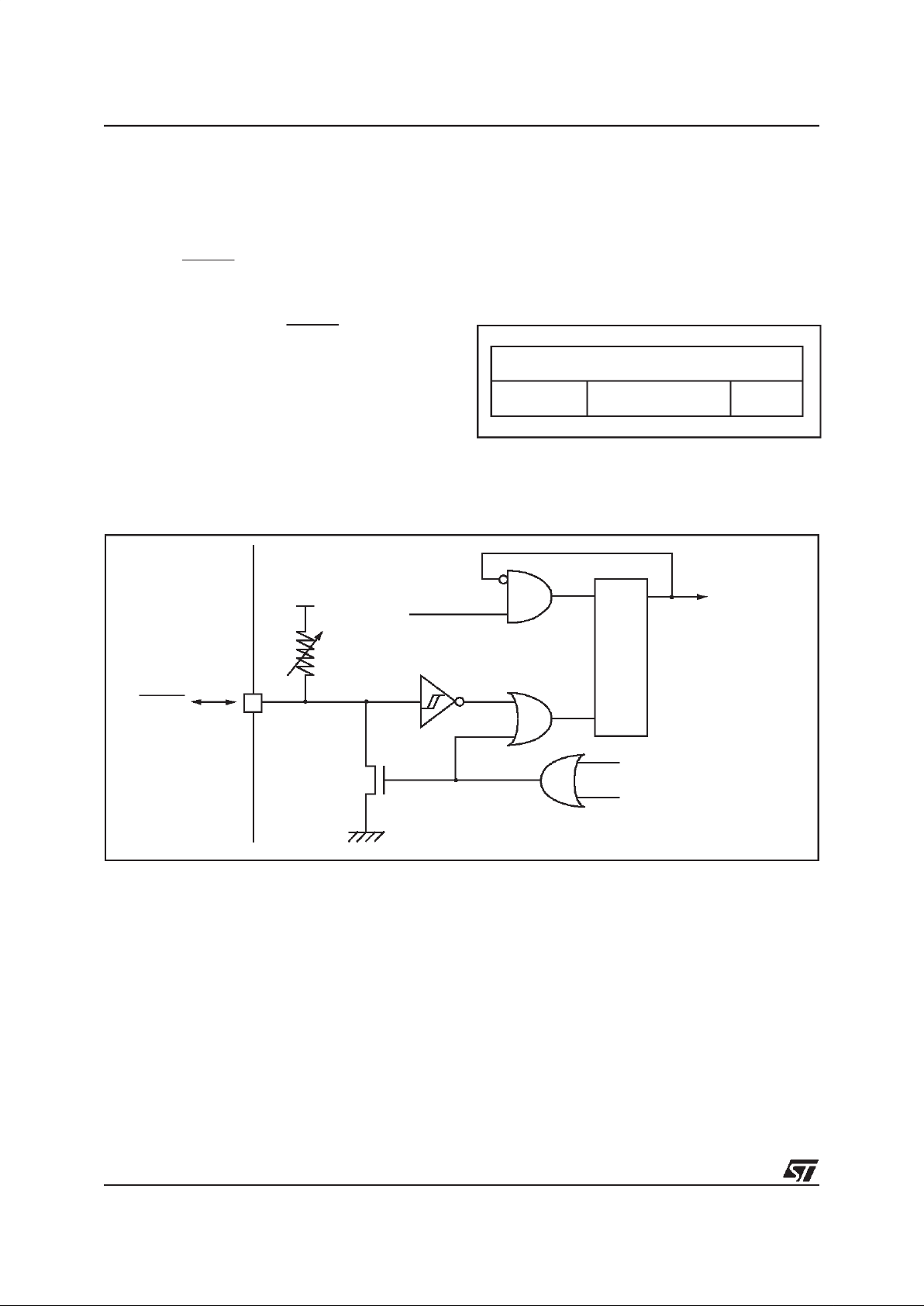
Figure 7. EEPROM Block Diagram
EECSR
EEPROM INTERRUPT
FALLING
EDGE
HIGH VOLTAGE
PUMP
IE LAT00000 PGM
EEPROMRESERVED
DETECTOR
EEPROM
MEMORY MATRIX
(1 ROW = 16 x 8 BITS)
ADDRESS
DECODER
DATA
MULTIPLEXER
16 x 8 BITS
DATA LATCHES
ROW
DECODER
DATA BUS
4
4
4
128128
ADDRESS BUS
ST72334J/N, ST72314J/N, ST72124J
18/148
DATA EEPROM (Cont’d)
6.3 MEMORY ACCESS
The Data EEPROM memory read/write access
modes are controlled by the LAT bit of the EEPROM Control/Status register (EECSR). The flowchart inFigure 8 describes these different memory
access modes.
Read Operation (LAT=0)
The EEPROM canbe read as a normal ROM location when the LAT bit of the EECSR register is
cleared. Ina read cycle, the byte to be accessed is
put onthedatabusin less than 1CPUclock cycle.
This means that reading data from EEPROM
takes the same time as reading data from
EPROM, but this memory cannot be used to execute machine code.
Write Operation (LAT=1)
To access the write mode, the LAT bit has to be
set by software (the PGM bit remains cleared).
When a write access to the EEPROM area occurs,
the value is latched inside the 16 data latches according to its address.
When PGM bit is set by the software, all the previous bytes written in the data latches(up to16) are
programmed in the EEPROM cells. The effective
high address (row) is determined by the last EEPROM write sequence. To avoid wrong programming, the user must take care that all the bytes
written between two programming sequences
have the same high address: only the four Least
Significant Bits of the address can change.
At the end of the programming cycle, the PGM and
LAT bits are cleared simultaneously, and an interrupt is generated if the IE bitis set. The Data EEPROM interrupt request is cleared by hardware
when the Data EEPROM interrupt vector is
fetched.
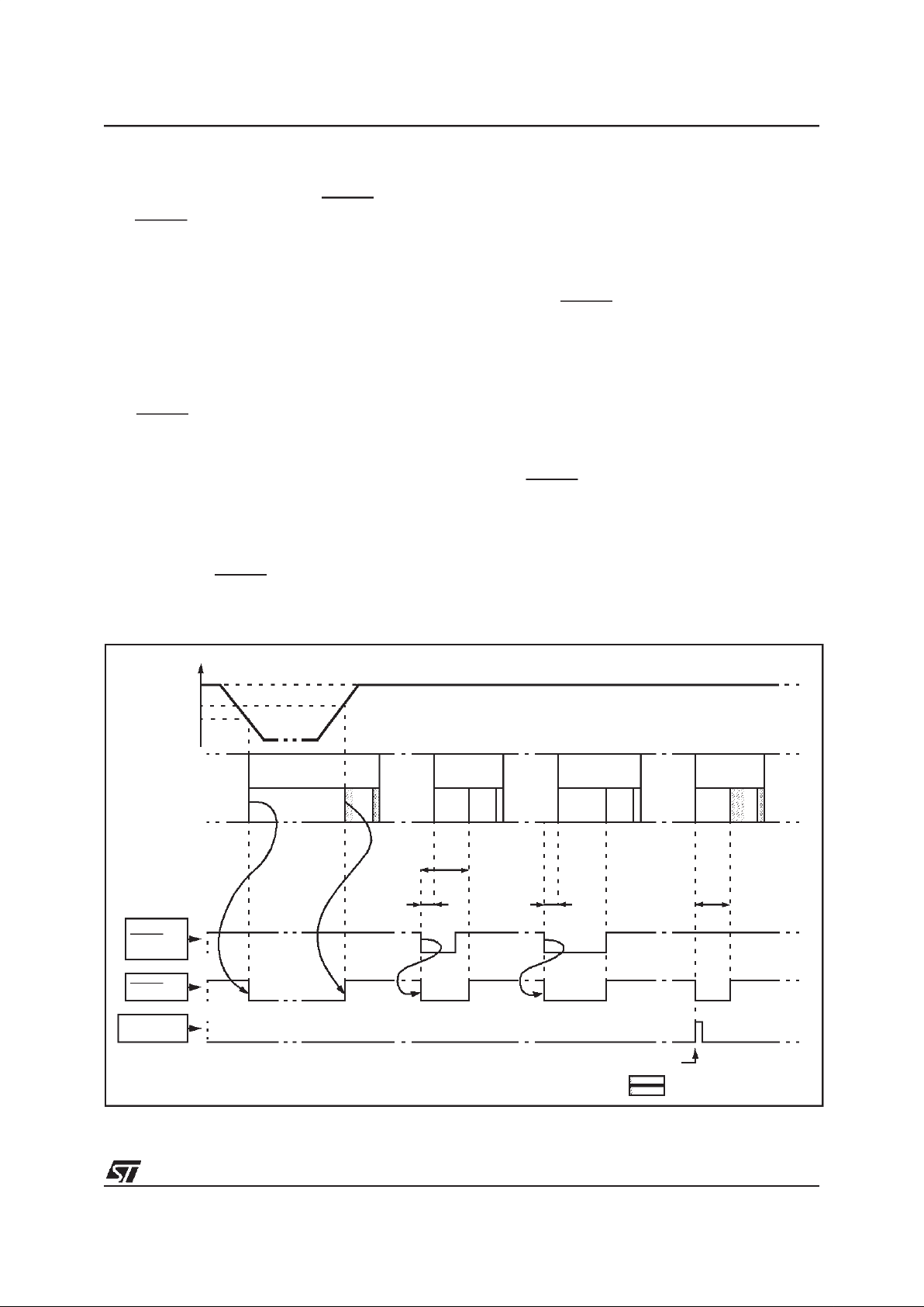
Note: Care should be taken during the programming cycle. Writing to the same memory location
will over-program the memory (logical AND between the two write access data result) because
the data latches are only cleared at the end of the
programming cycle and by thefalling edge of LAT
bit.
It is not possible toread the latched data.
This note is ilustrated by the Figure 9.
Figure 8. Data EEPROM ProgrammingFlowchart
READ MODE
LAT=0
PGM=0
WRITEMODE
LAT=1
PGM=0
READ BYTES
IN EEPROM AREA
WRITE UP TO 16 BYTES
IN EEPROM AREA
(with the same 12 MSB of the address)
START PROGRAMMING CYCLE
LAT=1
PGM=1 (set by software)
LAT
INTERRUPT GENERATION
IF IE=1 0 1
CLEARED BY HARDWARE
ST72334J/N, ST72314J/N, ST72124J
19/148
DATA EEPROM (Cont’d)
6.4 POWER SAVING MODES
Wait mode
The DATAEEPROMcan enter WAIT mode on execution of the WFI instruction of the microcontroller. The DATA EEPROM will immediately enter
this mode if there is no programming in progress,
otherwise the DATA EEPROM will finish the cycle
and then enter WAIT mode.
Halt mode
The DATA EEPROM immediatly enters HALT
mode if themicrocontroller executes the HALT instruction. Therefore the EEPROM will stop the
function in progress, and data may be corrupted.
6.5 ACCESS ERROR HANDLING
If a read access occurs while LAT=1, then the data
bus will not be driven.
If a write access occurs while LAT=0, then the
data on the bus will not be latched.
If a programming cycle is interrupted (by software/
RESET action), the memory data will not be guaranteed.
Figure 9. Data EEPROM ProgrammingCycle
LAT
ERASE CYCLE WRITE CYCLE
PGM
t
PROG
READ OPERATION NOT POSSIBLE
WRITE OF
DATA LATCHES
READ OPERATION POSSIBLE
INTERNAL
PROGRAMMING
VOLTAGE
EEPROM INTERRUPT

ST72334J/N, ST72314J/N, ST72124J
20/148
DATA EEPROM (Cont’d)
6.6 REGISTER DESCRIPTION
CONTROL/STATUS REGISTER (CSR)
Read/Write
Reset Value: 0000 0000 (00h)
Bit 7:3 = Reserved, forced by hardware to 0.
Bit 2 = IE
Interrupt enable
Thisbitissetandclearedbysoftware.Itenables the
Data EEPROM interrupt capability when the PGM
bit iscleared by hardware. The interrupt request is
automatically cleared when thesoftware enters the
interrupt routine.
0: Interrupt disabled
1: Interrupt enabled
Bit 1 = LAT
Latch Access Transfer
This bit is set by software. It is cleared by hardware at the end of the programming cycle. It can
only be cleared by software if PGM bit is cleared.
0: Read mode
1: Write mode
Bit 0 = PGM
Programming controland status
Thisbitis setbysoftware tobegin theprogramming
cycle. At the end of the programming cycle, this bit
isclearedby hardwareandaninterruptisgenerated
if theITE bit is set.
0: Programming finished or not yet started
1: Programming cycle isin progress
Note: if thePGM bit is cleared during the programming cycle, the memory data is not guaranteed
Table 3. DATA EEPROM Register Map and Reset Values
6.7 READ-OUT PROTECTION OPTION
The Data EEPROM can be optionally read-out
protected in ST72334 ROM devices (see option
list onpage 145). ST72C334 Flash devices do not
have this protection option.
70
00000IELATPGM
Address
(Hex.)
Register
Label
76543210
002Ch
EECSR
Reset Value
00000IE0
RWM
0
PGM
0
ST72334J/N, ST72314J/N, ST72124J
21/148
7 CENTRAL PROCESSING UNIT
7.1 INTRODUCTION
This CPU has a full 8-bit architecture and contains
six internal registers allowing efficient 8-bit data
manipulation.
7.2 MAIN FEATURES
■ 63 basic instructions
■ Fast 8-bit by 8-bit multiply
■ 17 main addressing modes
■ Two 8-bit index registers
■ 16-bit stack pointer
■ Low power modes
■ Maskable hardware interrupts
■ Non-maskable software interrupt
7.3 CPU REGISTERS
The 6 CPU registers shown in Figure 10 are not
present in the memory mapping and are accessed
by specific instructions.
Accumulator (A)
The Accumulator is an 8-bit general purpose register used to hold operands and the results of the
arithmetic and logic calculations and to manipulate
data.
Index Registers (X and Y)
In indexed addressing modes, these 8-bitregisters
are used to create either effective addresses or
temporary storage areas for data manipulation.
(The Cross-Assembler generates a precede instruction (PRE) to indicate that the following instruction refers to the Y register.)
The Y registeris not affectedby the interrupt automatic procedures (notpushed to and popped from
the stack).
Program Counter (PC)
The program counter is a 16-bit register containing
the address of the next instruction to be executed
by the CPU. It is made of two 8-bit registers PCL
(Program Counter Low which is the LSB) andPCH
(Program CounterHigh which is the MSB).
Figure 10. CPU Registers
ACCUMULATOR
X INDEX REGISTER
Y INDEX REGISTER
STACK POINTER
CONDITION CODE REGISTER
PROGRAM COUNTER
70
1C11HI NZ
RESET VALUE = RESET VECTOR @ FFFEh-FFFFh
70
70
70
0
7
15 8
PCH
PCL
15
87 0
RESET VALUE = STACKHIGHER ADDRESS
RESET VALUE =
1X11X1XX
RESET VALUE = XXh
RESET VALUE = XXh
RESET VALUE= XXh
X = Undefined Value

ST72334J/N, ST72314J/N, ST72124J
22/148
CPU REGISTERS (Cont’d)
CONDITION CODE REGISTER (CC)
Read/Write
Reset Value: 111x1xxx
The 8-bit Condition Code register contains the interrupt mask and four flags representative of the
result ofthe instruction just executed. This register
can also be handled by the PUSH and POP instructions.
These bits can be individually tested and/or controlled by specific instructions.
Bit 4 = H
Half carry
.
This bit is set by hardware whena carryoccursbetween bits 3 and 4 of the ALU during an ADD or
ADC instruction. It is reset by hardware during the
same instructions.
0: No half carry has occurred.
1: A half carry has occurred.
This bit is tested using the JRH or JRNH instruction. The H bit is useful in BCD arithmetic subroutines.
Bit 3 = I
Interrupt mask
.
This bit is set by hardware when entering in interrupt or by software to disable all interrupts except
the TRAP software interrupt. This bit is cleared by
software.
0: Interrupts are enabled.
1: Interrupts are disabled.
This bit is controlledby the RIM, SIM and IRET instructions and is tested by the JRM and JRNM instructions.
Note: Interrupts requested while I is set are
latched and can be processed when I is cleared.
By default an interrupt routine is not interruptable
because the I bit is set by hardware when you enter it and resetby the IRETinstruction at the endof
the interrupt routine. If the I bit is cleared by software in the interrupt routine, pending interrupts are
serviced regardless of the priority level of the current interrupt routine.
Bit 2 = N
Negative
.
This bit is set and cleared by hardware. It is representative of the result sign of the last arithmetic,
logical or data manipulation. It is a copy of the 7
th
bit of the result.
0:Theresultof the last operation is positive or null.
1: The result of the last operation is negative
(i.e. the most significant bit is a logic 1).
This bit isaccessed bythe JRMI andJRPL instructions.
Bit 1 = Z
Zero
.
This bit is set and cleared by hardware. Thisbit indicates that the result of the last arithmetic, logical
or data manipulation is zero.
0: The result of the last operation is different from
zero.
1: The result of the last operation is zero.
This bit is accessed by the JREQ and JRNE test
instructions.
Bit 0 = C
Carry/borrow.
This bit is set and cleared by hardware and software. It indicates an overflow or an underflow has
occurred during the last arithmetic operation.
0: No overflow or underflow has occurred.
1: An overflow or underflow hasoccurred.
This bit is driven by the SCF and RCF instructions
and tested by the JRC and JRNC instructions. It is
also affected by the “bit test and branch”, shift and
rotate instructions.
70
111HINZC
ST72334J/N, ST72314J/N, ST72124J
23/148
CENTRAL PROCESSING UNIT (Cont’d)
Stack Pointer (SP)
Read/Write
Reset Value: 01 FFh
The Stack Pointer is a 16-bit register which is always pointingto the next free location in the stack.
It isthen decremented after data has been pushed
onto the stack and incremented before data is
popped from the stack (see Figure 11).
Since the stack is 256 bytes deep, the 8th most
significant bits are forced by hardware. Following
an MCU Reset, or after a Reset Stack Pointer instruction (RSP), the Stack Pointer contains its reset value (the SP7 to SP0 bits areset) which is the
stack higher address.
The least significant byte of the Stack Pointer
(called S) can be directly accessed by a LD instruction.
Note: When the lower limit is exceeded, the Stack
Pointer wraps around to the stack upper limit, without indicating the stack overflow. The previously
stored information is then overwritten and therefore lost. The stack also wrapsin case of anunderflow.
The stack is used to save the return address during a subroutine call and the CPU context during
an interrupt. The user may also directly manipulate
the stack by meansof the PUSH and POP instructions. In the case of an interrupt, the PCL is stored
at the first location pointed to by the SP. Then the
other registers are stored in the next locations as
shown in Figure 11.
– When an interrupt is received, the SP is decre-
mented and the context is pushed on the stack.
– On return from interrupt, the SP is incremented
and the context is popped from thestack.
A subroutine call occupies twolocations and an interrupt five locations in the stack area.
Figure 11. Stack Manipulation Example
15 8
00000001
70
SP7 SP6 SP5 SP4 SP3 SP2 SP1 SP0
PCH
PCL
SP
PCH
PCL
SP
PCL
PCH
X
A
CC
PCH
PCL
SP
PCL
PCH
X
A
CC
PCH
PCL
SP
PCL
PCH
X
A
CC
PCH
PCL
SP
SP
Y
CALL
Subroutine
Interrupt
Event
PUSH Y POP Y IRET
RET
or RSP
@ 01FFh
@ 0100h
Stack Higher Address = 01FFh
Stack Lower Address =
0100h
ST72334J/N, ST72314J/N, ST72124J
24/148
8 SUPPLY, RESET AND CLOCK MANAGEMENT
The ST72334J/N, ST72314J/N and ST72124J microcontrollers include a range of utility features for
securing the application in critical situations (for
example in case of a power brown-out), and reducing the number of external components. An
overview is shown in Figure 12.
See Section 15 ”ELECTRICAL CHARACTERISTICS” on page 105 for more details.
Main Features
■ Supply Manager with main supply low voltage
detection (LVD)
■ Reset Sequence Manager (RSM)
■ Multi-Oscillator (MO)
– 4 Crystal/Ceramic resonator oscillators
– 1 External RC oscillator
– 1 Internal RC oscillator
■ Clock Security System (CSS)
– Clock Filter
– Backup Safe Oscillator
Figure 12. Clock, Reset and Supply Block Diagram
IE D00 0 0 RF RF
CRSR
CSS WDG
f
OSC
CSS INTERRUPT
LVD
LOW VOLTAGE
DETECTOR
(LVD)
MULTI-
OSCILLATOR
(MO)
FROM
WATCHDOG
PERIPHERAL
OSC1
RESET
VDD
VSS
RESET SEQUENCE
MANAGER
(RSM)
CLOCK
FILTER
SAFE
OSC
CLOCK SECURITYSYSTEM
(CSS)
OSC2
TO
MAIN CLOCK
CONTROLLER
ST72334J/N, ST72314J/N, ST72124J
25/148
8.1 LOW VOLTAGE DETECTOR (LVD)
To allow the integration of power management
features in the application, the Low Voltage Detector function (LVD) generates a static reset when
the VDDsupply voltage is below a V
IT-
reference
value. This means that it secures the power-up as
well as the power-down keeping the ST7 in reset.
The V
IT-
referencevalue fora voltage drop is lower
than the V
IT+
referencevalue forpower-on in order
to avoid a parasitic reset when theMCUstarts running and sinks current on the supply (hysteresis).
The LVD Reset circuitry generates a reset when
VDDis below:
–V
IT+
when VDDis rising
–V
IT-
when VDDis falling
The LVD function is illustrated in the Figure 13.
Provided the minimum VDDvalue (guaranteed for
the oscillator frequency) is above V
IT-
, the MCU
can only be in two modes:
– under full software control
– in static safe reset
In these conditions, secure operation is always ensured for the application without the need for external reset hardware.
During aLow Voltage Detector Reset, the RESET
pin is held low, thus permitting the MCU to reset
other devices.
Notes:
1. The LVD allows the device to be used without
any external RESET circuitry.
2. Three different reference levels are selectable
through the option byte according to the application requirement.
LVD application note
Application software can detect a reset caused by
the LVD by reading the LVDRF bit in the CRSR
register.
This bit is set by hardware when a LVD reset is
generated and cleared by software (writing zero).
Figure 13. Low Voltage Detector vs Reset
V
DD
V
IT+
RESET
V
IT-
V
hyst
ST72334J/N, ST72314J/N, ST72124J
26/148
8.2 RESET SEQUENCE MANAGER (RSM)
8.2.1 Introduction
The reset sequence manager includes three RESET sources as shown in Figure 15:
■ External RESET source pulse
■ Internal LVD RESET (Low Voltage Detection)
■ Internal WATCHDOG RESET
These sources act on the RESET pin and it is always kept low during the delay phase.
The RESET service routine vector is fixed at addresses FFFEh-FFFFh in the ST7 memory map.
The basic RESET sequence consists of 3 phases
as shown in Figure 14:
■ Delay depending on the RESET source
■ 4096 CPU clock cycle delay
■ RESET vector fetch
The 4096 CPU clock cycle delay allows the oscillator to stabilise and ensures that recovery has
taken place from the Reset state.
The RESET vector fetch phase duration is 2 clock
cycles.
Figure 14. RESET Sequence Phases
Figure 15. Reset Block Diagram
RESET
DELAY
INTERNAL RESET
4096 CLOCK CYCLES
FETCH
VECTOR
f
CPU
COUNTER
RESET
R
ON
V
DD
WATCHDOG RESET
LVD RESET
INTERNAL
RESET
ST72334J/N, ST72314J/N, ST72124J
27/148
RESET SEQUENCE MANAGER (Cont’d)
8.2.2 Asynchronous External RESET pin
The RESETpin is both an input andan open-drain
output with integrated RONweak pull-up resistor.
This pull-up has no fixed value but varies in accordance with the input voltage. It can be pulled
low by external circuitry to reset the device. See
electrical characteristics section for more details.
A RESET signal originating from an external
source must have a duration of at least t
h(RSTL)in
in
order to be recognized. This detection is asynchronous and therefore the MCU can enter reset state
even in HALT mode.
The RESET pin is an asynchronous signal which
plays a major role in EMS performance. In a noisy
environment, it is recommended to follow the
guidelines mentioned in the electrical characteristics section.
Two RESET sequences can be associated with
this RESET source: short or long external reset
pulse (see Figure 16).
Starting from the external RESET pulse recognition, the device RESET pin acts as an output that
is pulled low during at least t
w(RSTL)out
.
8.2.3 Internal Low Voltage Detection RESET
Two different RESET sequences caused by the internal LVD circuitry can be distinguished:
■ Power-On RESET
■ Voltage Drop RESET
The device RESET pin acts as an output that is
pulled low when VDD<V
IT+
(rising edge) or
VDD<V
IT-
(falling edge) as shown in Figure 16.
The LVD filters spikes on VDDlarger than t
g(VDD)
to
avoid parasitic resets.
8.2.4 Internal Watchdog RESET
The RESET sequence generated by a internal
Watchdog counter overflow is shown in Figure 16.
Starting from the Watchdog counter underflow, the
device RESET pin acts as an output that is pulled
low during at least t
w(RSTL)out
.
Figure 16. RESET Sequences
V
DD
RUN
RESET PIN
EXTERNAL
WATCHDOG
DELAY
V
IT+
V
IT-
t
h(RSTL)in
t
w(RSTL)out
RUN
DELAY
t
h(RSTL)in
DELAY
WATCHDOG UNDERFLOW
t
w(RSTL)out
RUN RUN
DELAY
RUN
RESET
RESET
SOURCE
SHORT EXT.
RESET
LVD
RESET
LONG EXT.
RESET
WATCHDOG
RESET
INTERNAL RESET (4096T
CPU
)
FETCH VECTOR
ST72334J/N, ST72314J/N, ST72124J
28/148
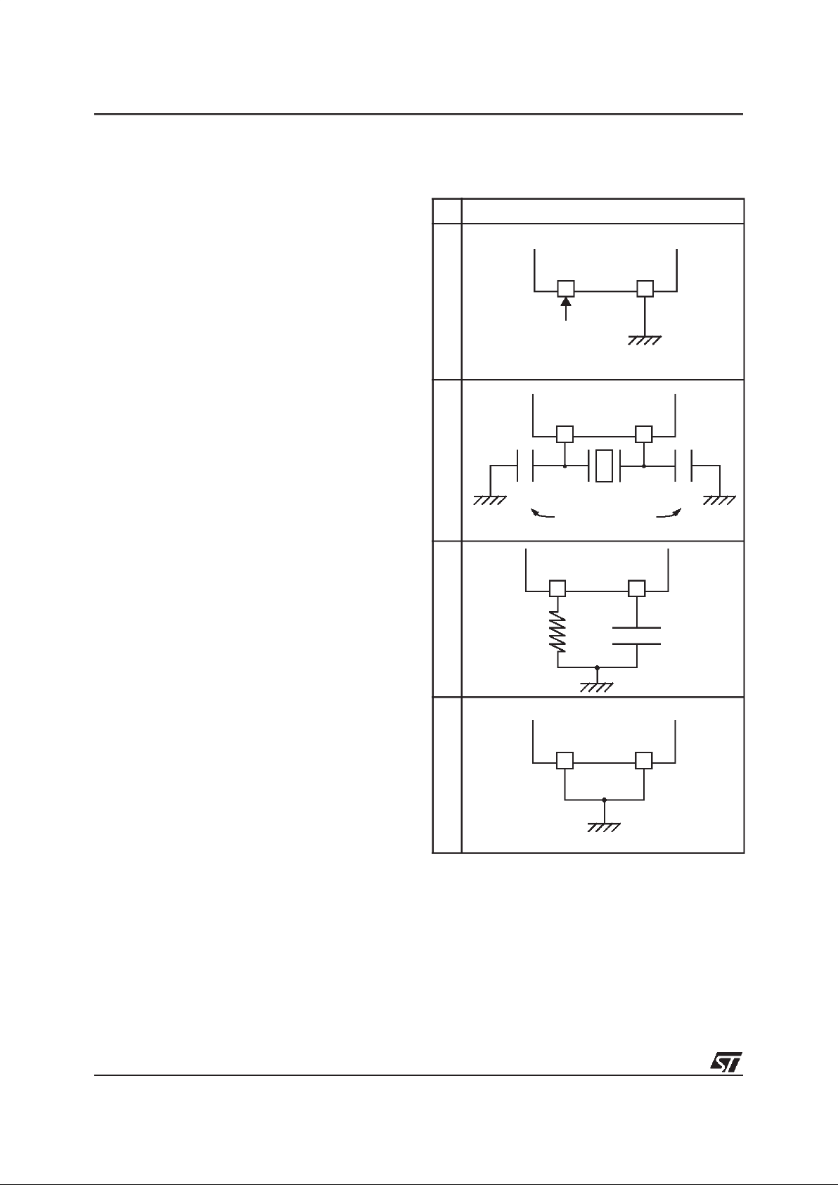
8.3 MULTI-OSCILLATOR (MO)
The main clock of the ST7 can be generated by
four different source types coming from the multioscillator block:
■ an external source
■ 4 crystal or ceramic resonator oscillators
■ an external RC oscillator
■ an internal high frequency RC oscillator
Each oscillator is optimized for a given frequency
range in terms of consumption and is selectable
through the option byte. The associated hardware
configuration are shown in Table 4. Refer to the
electrical characteristics section for more details.
External Clock Source
In this external clock mode, a clock signal (square,
sinus ortriangle) with~50% duty cycle has todrive
the OSC1 pinwhile theOSC2 pinis tied to ground.
Crystal/Ceramic Oscillators
This family of oscillators has theadvantage of producing a very accurate rate on the main clock of
the ST7. The selection within a list of 4 oscillators
with different frequency ranges has to be done by
option byte in order to reduce consumption. In this
mode of the multi-oscillator, the resonatorand the
load capacitors have to be placed as close as possible to the oscillator pins in order to minimize output distortion and start-up stabilization time. The
loading capacitance values must be adjusted according to the selected oscillator.
These oscillators are not stopped during the
RESET phase to avoid losing time in the oscillator
start-up phase.
External RC Oscillator
This oscillator allows a low cost solution for the
main clockof the ST7 using only an external resistor and anexternal capacitor.The frequencyof the
external RC oscillator (in the range of some MHz.)
is fixed by the resistor and the capacitor values.
Consequently in this MO mode, the accuracy of
the clock is directly linked to the accuracy of the
discrete components.
Internal RC Oscillator
The internal RC oscillator mode is based on the
same principle as the external RC oscillator including the resistance and the capacitance of the device. This mode is the most cost effective one with
the drawback of a lower frequency accuracy. Its
frequency is in the range of several MHz.
In this mode, the two oscillator pins have to be tied
to ground.
Table 4. ST7 Clock Sources
Hardware Configuration
External ClockCrystal/Ceramic ResonatorsExternal RC OscillatorInternal RC Oscillator
OSC1 OSC2
EXTERNAL
ST7
SOURCE
OSC1 OSC2
LOAD
CAPACITORS
ST7
C
L2
C
L1
OSC1 OSC2
ST7
C
EX
R
EX
OSC1 OSC2
ST7
ST72334J/N, ST72314J/N, ST72124J
29/148
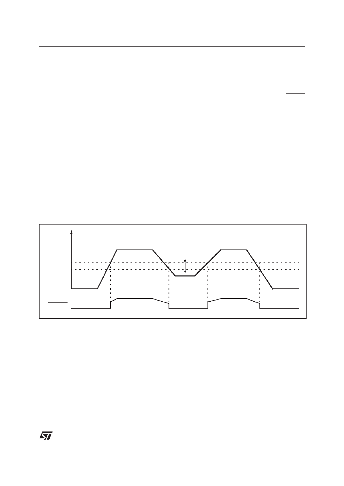
8.4 CLOCK SECURITY SYSTEM (CSS)
The Clock Security System (CSS) protects the
ST7 against main clock problems. To allow the integration of the security features in the applications, itis based on a clock filter control and anInternal safe oscillator. The CSS can be enabled or
disabled by option byte.
8.4.1 Clock Filter Control
The clock filter is based on a clock frequency limitation function.
This filter function is able to detect and filter high
frequency spikes on the ST7 main clock.
If the oscillator is not working properly (e.g. working at a harmonic frequency of the resonator), the
current active oscillator clock can be totally filtered, and then no clock signal is available for the
ST7 from this oscillator anymore. If the original
clock source recovers, the filtering is stopped automatically and the oscillator supplies the ST7
clock.
8.4.2 Safe Oscillator Control
The safe oscillator of the CSS block is a low frequency back-up clock source (see Figure 17).
If the clock signal disappears (due to a broken or
disconnected resonator...) during a safe oscillator
period, the safe oscillator delivers a low frequency
clock signalwhich allows the ST7 to perform some
rescue operations.
Automatically, theST7 clock sourceswitches back
from the safe oscillator if the original clock source
recovers.
Limitation detection
The automatic safe oscillator selection is notified
by hardware setting the CSSD bit of the CRSR
register. An interrupt can be generated if the CSSIE bit has been previously set.
These two bits are described in the CRSR register
description.
8.4.3 Low Power Modes
8.4.4 Interrupts
The CSS interrupt event generates an interrupt if
the corresponding Enable Control Bit (CSSIE) is
set and the interrupt mask in the CC register is reset (RIM instruction).
Figure 17. Clock Filter Function and Safe Oscillator Function
Mode Description
WAIT
No effect on CSS. CSS interrupt cause the
device to exit from Wait mode.
HALT
The CRSR register is frozen. The CSS (including the safe oscillator) is disabled until
HALT mode is exited.The previous CSS
configuration resumes when the MCU is
woken up by aninterrupt with “exit from
HALT mode” capability or from the counter
reset value when the MCU is woken up by a
RESET.
Interrupt Event
Event
Flag
Enable
Control
Bit
Exit
from
Wait
Exit
from
Halt
CSS event detection
(safe oscillator activated as main clock)
CSSD CSSIE Yes No
f
OSC
/2
f
CPU
f
OSC
/2
f
CPU
f
SFOSC
SAFE OSCILLATOR
FUNCTION
CLOCK FILTER
FUNCTION
ST72334J/N, ST72314J/N, ST72124J
30/148
8.5 SUPPLY, RESET AND CLOCK REGISTER DESCRIPTION
Read/Write
Reset Value: 000x 000x (xxh)
Bit 7:5 = Reserved, always read as 0.
Bit 4 = LVDRF
LVD reset flag
This bit indicates that the last RESET was generated by the LVD block. It is set by hardware (LVD
reset) and cleared by software (writing zero). See
WDGRF flag description for more details. When
the LVD is disabled by option byte, the LVDRF bit
value is undefined.
Bit 3 = Reserved, always read as 0.
Bit 2 = CSSIE
Clock security syst.interrupt enable
This bit enables the interrupt when a disturbance
is detected bythe clock security system (CSSD bit
set). It is set and cleared by software.
0: Clock security system interrupt disabled
1: Clock security system interrupt enabled
Refer to Table 6, “Interrupt Mapping,” on page 32
for more details on the CSS interrupt vector. When
the CSS is disabled by option byte, the CSSIE bit
has no effect.
Bit 1 = CSSD
Clock security system detection
This bit indicates that the safe oscillator of the
clock security system block has been selected by
hardware due to a disturbance on the main clock
signal (f
OSC
). It is set by hardware and cleared by
reading the CRSR register when the originaloscillator recovers.
0: Safe oscillator is not active
1: Safe oscillator has been activated
When the CSS is disabled by option byte, the
CSSD bit value is forced to 0.
Bit 0 = WDGRF
Watchdog reset flag
This bit indicates that the last RESET was generated by the watchdog peripheral. It is set by hardware (Watchdog RESET) and cleared by software
(writing zero) or an LVD RESET (to ensure a stable cleared state of the WDGRF flag when the
CPU starts).
Combined with the LVDRF flag information, the
flag description is given by the following table.
Application notes
The LVDRF flag is not cleared when another RESET type occurs (external or watchdog), the
LVDRF flagremains set to keep trace of the original failure.
In this case, a watchdog reset can be detected by
software while an external reset can not.
Table 5. Clock, Reset and Supply Register Map and Reset Values
70
000
LVD
RF
0
CSSIECSSDWDG
RF
RESET Sources LVDRF WDGRF
External RESET pin 0 0
Watchdog 0 1
LVD 1 X
Address
(Hex.)
Register
Label
76543210
002Bh
CRSR
Reset Value 0 0 0
LVDRF
x0
CFIE
0
CSSD0WDGRF
x

ST72334J/N, ST72314J/N, ST72124J
31/148
9 INTERRUPTS
The ST7 core may be interruptedby one oftwo different methods: maskable hardware interrupts as
listed in the Interrupt Mapping Table and a nonmaskable software interrupt (TRAP). The Interrupt
processing flowchart is shown in Figure 18.
The maskableinterrupts must be enabled clearing
the I bit in order to be serviced. However, disabled
interrupts may be latched and processed when
they are enabled (see external interrupts subsection).
When an interrupt has to be serviced:
– Normal processing is suspended at the end of
the current instruction execution.
– The PC, X, A and CC registers are saved onto
the stack.
– The I bit of the CC register is set to prevent addi-
tional interrupts.
– ThePC isthenloaded with the interrupt vectorof
the interruptto service and the first instruction of
the interrupt service routine is fetched (refer to
the Interrupt Mapping Tablefor vector addresses).
The interrupt service routine should finish with the
IRET instruction which causes the contents of the
saved registers to be recovered from thestack.
Note: As a consequence of the IRET instruction,
the I bit will be cleared and the main program will
resume.
Priority management
By default, a servicing interrupt cannot be interrupted because the I bit is set by hardware entering in interrupt routine.
In the case when severalinterrupts are simultaneously pending, an hardware priority defines which
one will be serviced first (see the Interrupt Mapping Table).
Interrupts and Low power mode
All interrupts allow the processor to leave the
WAIT low power mode. Only external and specifically mentioned interrupts allow the processor to
leave the HALT low power mode (refer to the “Exit
from HALT“ column in the Interrupt Mapping Table).
9.1 NON MASKABLE SOFTWARE INTERRUPT
This interrupt is entered when the TRAP instruction is executed regardless of the stateof theI bit.
It will be serviced according to the flowchart on
Figure 18.
9.2 EXTERNAL INTERRUPTS
External interrupt vectors can be loaded into the
PC register if the corresponding external interrupt
occurred and if the I bit is cleared. Theseinterrupts
allow the processor to leave the Halt low power
mode.
The external interrupt polarity is selected through
the miscellaneous register or interrupt register (if
available).
An external interrupt triggered on edge will be
latched and the interrupt request automatically
cleared upon entering the interrupt serviceroutine.
If several input pins, connected to the same interrupt vector, are configured as interrupts, their signals are logically ANDed beforeentering the edge/
level detection block.
Caution:The type of sensitivitydefinedin the Miscellaneous or Interrupt register (if available) applies to the ei source. In case of an ANDedsource
(as described on the I/O ports section), a low level
on an I/O pin configured as input with interrupt,
masks the interrupt requesteven in case of risingedge sensitivity.
9.3 PERIPHERAL INTERRUPTS
Different peripheral interrupt flags in the status
register are able to cause an interrupt when they
are active if both:
– The I bit of the CC register is cleared.
– Thecorresponding enable bit is setin thecontrol
register.
If any of these two conditions is false, the interrupt
is latched and thus remains pending.
Clearing an interrupt request is done by:
– Writing “0” to the corresponding bit in the status
register or
– Access tothe status registerwhile the flag isset
followed by a read or write of an associated register.
Note: the clearing sequence resets the internal
latch. A pending interrupt (i.e. waiting for being enabled) will therefore be lost ifthe clear sequence is
executed.

ST72334J/N, ST72314J/N, ST72124J
32/148
INTERRUPTS (Cont’d)
Figure 18. Interrupt Processing Flowchart
Table 6. Interrupt Mapping
N°
Source
Block
Description
Register
Label
Priority
Order
Exit
from
HALT
Address
Vector
RESET Reset
N/A
Highest
Priority
Lowest
Priority
yes FFFEh-FFFFh
TRAP Software Interrupt no FFFCh-FFFDh
0 Not used FFFAh-FFFBh
1
MCC/RTC
CSS
Main Clock Controller Time Base Interrupt
or Clock Security System Interrupt
MCCSR
CRSR
yes
FFF8h-FFF9h
2 ei0 External Interrupt Port A3..0
N/A
FFF6h-FFF7h
3 ei1 External Interrupt Port F2..0 FFF4h-FFF5h
4 ei2 External Interrupt Port B3..0 FFF2h-FFF3h
5 ei3 External Interrupt Port B7..4 FFF0h-FFF1h
6 Not used FFEEh-FFEFh
7 SPI SPI Peripheral Interrupts SPISR
no
FFECh-FFEDh
8 TIMER A TIMER A Peripheral Interrupts TASR FFEAh-FFEBh
9 TIMER B TIMER B Peripheral Interrupts TBSR FFE8h-FFE9h
10 SCI SCI Peripheral Interrupts SCISR FFE6h-FFE7h
11 Data-EEPROM Data EEPROM Interrupt EECSR FFE4h-FFE5h
12
Not used
FFE2h-FFE3h
13 FFE0h-FFE1h
I BIT SET?
Y
N
IRET?
Y
N
FROM RESET
LOAD PC FROM INTERRUPT VECTOR
STACK PC, X, A, CC
SET I BIT
FETCH NEXT INSTRUCTION
EXECUTEINSTRUCTION
THIS CLEARS I BIT BY DEFAULT
RESTORE PC,X, A,CC FROM STACK
INTERRUPT
Y
N
PENDING?

ST72334J/N, ST72314J/N, ST72124J
33/148
10 POWER SAVING MODES
10.1 INTRODUCTION
To give a large measure of flexibilitytotheapplication in terms of power consumption, four main
power saving modes are implemented in the ST7
(see Figure 19): SLOW, WAIT (SLOW WAIT), ACTIVE HALT and HALT.
After a RESET the normal operating mode is selected by default (RUN mode). This mode drives
the device (CPU and embedded peripherals) by
means of a master clock which is based on the
main oscillator frequency divided by 2 (f
CPU
).
From RUN mode, the different power saving
modes may be selected by setting the relevant
register bits or by calling the specific ST7 software
instruction whose action depends on the the oscillator status.
Figure 19. Power Saving Mode Transitions
10.2 SLOW MODE
This mode has two targets:
– To reduce powerconsumption bydecreasingthe
internal clock in the device,
– To adapt the internal clock frequency (f
CPU
)to
the available supply voltage.
SLOW mode is controlled by three bits in the
MISCR1 register: the SMS bit which enables or
disables Slow mode and two CPx bits whichselect
the internal slow frequency (f
CPU
).
In this mode, the oscillator frequency can bedivided by 4, 8, 16 or 32 instead of 2 in normal operating mode. The CPU and peripherals are clocked at
this lower frequency.
Note: SLOW-WAIT modeis activated when enterring the WAIT mode while the device is already in
SLOW mode.
Figure 20. SLOW Mode Clock Transitions
POWER CONSUMPTION
WAIT
SLOW
RUN
ACTIVE HALT
High
Low
SLOW WAIT
HALT
00 01
SMS
CP1:0
f
CPU
NEW SLOW
NORMAL RUN MODE
MISCR1
FREQUENCY
REQUEST
REQUEST
f
OSC
/2
f
OSC
/4 f
OSC
/8 f
OSC
/2

ST72334J/N, ST72314J/N, ST72124J
34/148
POWER SAVING MODES (Cont’d)
10.3 WAIT MODE
WAIT mode places the MCU in a low power consumption mode by stopping the CPU.
This power saving mode is selectedby calling the
‘WFI’ instruction.
All peripherals remain active. During WAIT mode,
the I bit of the CC register is cleared, to enable all
interrupts. All other registers and memory remain
unchanged. The MCU remains inWAIT modeuntil
an interrupt or RESET occurs, whereupon the Program Counter branches to the starting address of
the interrupt or Reset service routine.
The MCU will remain in WAIT mode until a Reset
or an Interrupt occurs, causing it to wake up.
Refer to Figure21.
Figure 21. WAIT Mode Flow-chart
Note:
1. Before servicing an interrupt, the CC register is
pushed on the stack. The I bit of the CCregister is
set during the interrupt routine and cleared when
the CC register is popped.
WFI INSTRUCTION
RESET
INTERRUPT
Y
N
N
Y
CPU
OSCILLATOR
PERIPHERALS
I BIT
ON
ON
0
OFF
FETCH RESET VECTOR
OR SERVICE INTERRUPT
CPU
OSCILLATOR
PERIPHERALS
I BIT
ON
OFF
0
ON
CPU
OSCILLATOR
PERIPHERALS
I BIT
ON
ON
X
1)
ON
4096 CPU CLOCK CYCLE
DELAY

ST72334J/N, ST72314J/N, ST72124J
35/148
POWER SAVING MODES (Cont’d)
10.4 ACTIVE-HALT AND HALT MODES
ACTIVE-HALT and HALT modes are the two lowest power consumption modes of the MCU. They
are both entered by executing the ‘HALT’ instruction. Thedecision to enter eitherin ACTIVE-HALT
or HALT mode is given by the MCC/RTC interrupt
enable flag (OIE bit in MCCSR register).
10.4.1 ACTIVE-HALT MODE
ACTIVE-HALT mode is the lowest power consumption mode of the MCU with a real time clock
available. It is entered by executing the ‘HALT’ instruction when the OIE bit of the Main Clock Controller Statusregister (MCCSR) is set (see Section
13.2 ”MAIN CLOCK CONTROLLER WITH REAL
TIME CLOCKTIMER (MCC/RTC)” on page 50 for
more details on the MCCSR register).
The MCU can exit ACTIVE-HALT mode on reception of either an MCC/RTC interrupt, a specific interrupt (see Table 6, “Interrupt Mapping,” on
page 32) or a RESET. When exiting ACTIVEHALT mode by means of a RESET or an interrupt,
a 4096 CPU cycle delay occurs. After the start up
delay, the CPU resumes operation by servicing
the interrupt or by fetching the reset vector which
woke it up (see Figure23).
When entering ACTIVE-HALT mode, the I bit in
the CC register is cleared to enable interrupts.
Therefore, if an interrupt is pending, the MCU
wakes up immediately.
In ACTIVE-HALT mode, only the main oscillator
and its associated counter (MCC/RTC) are running to keep a wake-up time base. All other peripherals are not clocked except those which get their
clock supply from another clock generator (such
as external or auxiliary oscillator).
The safeguard against staying locked in ACTIVEHALT mode is provided by the oscillator interrupt.
Note: As soon as the interrupt capability of one of
the oscillators is selected (MCCSR.OIE bit set),
entering ACTIVE-HALT modewhile the Watchdog
is active does not generate a RESET.
This means that the device cannot spend more
than a defined delay in this power saving mode.
Figure 22. ACTIVE-HALT Timing Overview
Figure 23. ACTIVE-HALT Mode Flow-chart
Notes:
1. Peripheral clocked with an external clock source
can still be active.
2. Only the MCC/RTC interrupt and some specific
interrupts can exit the MCU from ACTIVE-HALT
mode (such as external interrupt). Refer to
Table 6, “Interrupt Mapping,” on page 32 for more
details.
3. Before servicing an interrupt, the CC register is
pushed on the stack. The I bit of the CCregister is
set during the interrupt routine and cleared when
the CC register is popped.
MCCSR
OIE bit
Power Saving Mode entered when HALT
instruction is executed
0 HALT mode
1 ACTIVE-HALT mode
HALTRUN RUN
4096 CPU CYCLE
DELAY
RESET
OR
INTERRUPT
HALT
INSTRUCTION
FETCH
VECTOR
ACTIVE
[MCCSR.OIE=1]
HALT INSTRUCTION
RESET
INTERRUPT
2)
Y
N
N
Y
CPU
OSCILLATOR
PERIPHERALS
1)
I BIT
ON
OFF
0
OFF
FETCH RESET VECTOR
OR SERVICE INTERRUPT
CPU
OSCILLATOR
PERIPHERALS
1)
I BIT
ON
OFF
X
3)
ON
CPU
OSCILLATOR
PERIPHERALS
I BITS
ON
ON
X
3)
ON
4096 CPU CLOCK CYCLE
DELAY
(MCCSR.OIE=1)

ST72334J/N, ST72314J/N, ST72124J
36/148
POWER SAVING MODES (Cont’d)
10.4.2 HALT MODE
The HALT mode is the lowest power consumption
mode of the MCU. It is entered by executing the
‘HALT’ instruction when the OIE bit of the Main
Clock Controller Status register (MCCSR) is
cleared (see Section 13.2 ”MAIN CLOCK CONTROLLER WITH REAL TIME CLOCK TIMER
(MCC/RTC)” on page 50 for more details on the
MCCSR register).
The MCU can exit HALT mode on reception of either a specific interrupt (see Table 6, “Interrupt
Mapping,” on page 32) or a RESET. When exiting
HALT mode by means of a RESET or an interrupt,
the oscillator is immediately turned on and the
4096 CPU cycle delay is used to stabilize the oscillator. After the start up delay, the CPU resumes
operation by servicing the interrupt or by fetching
the reset vector which woke it up (see Figure 25).
When entering HALT mode, the I bit in the CC register is forced to 0 to enable interrupts. Therefore,
if an interrupt is pending, the MCU wakes immediately.
In HALT mode, the main oscillator is turned off
causing all internal processing to be stopped, including the operation of the on-chip peripherals.
All peripherals are not clocked except the ones
which get their clock supply from another clock
generator (such as an external or auxiliary oscillator).
The compatibility of Watchdog operation with
HALT mode is configured by the “WDGHALT” option bit of the option byte. The HALT instruction
when executed while the Watchdog system is enabled, can generate a Watchdog RESET (see
Section 17.1 on page 143 for more details).
Figure 24. HALT Timing Overview
Figure 25. HALT Mode Flow-chart
Notes:
1. WDGHALTis anoption bit. See option byte sec-
tion for more details.
2. Peripheral clocked with an external clock source
can still be active.
3. Only some specific interrupts can exit the MCU
from HALT mode (such as external interrupt). Refer to Table 6, “Interrupt Mapping,” on page 32 for
more details.
4. Before servicing an interrupt, the CC register is
pushed on the stack. The I bit of the CCregister is
set during the interrupt routine and cleared when
the CC register is popped.
HALTRUN RUN
4096 CPU CYCLE
DELAY
RESET
OR
INTERRUPT
HALT
INSTRUCTION
FETCH
VECTOR
[MCCSR.OIE=0]
HALT INSTRUCTION
RESET
INTERRUPT
3)
Y
N
N
Y
CPU
OSCILLATOR
PERIPHERALS
2)
I BIT
OFF
OFF
0
OFF
FETCH RESET VECTOR
OR SERVICE INTERRUPT
CPU
OSCILLATOR
PERIPHERALS
I BIT
ON
OFF
X
4)
ON
CPU
OSCILLATOR
PERIPHERALS
I BITS
ON
ON
X
4)
ON
4096 CPU CLOCK CYCLE
DELAY
WATCHDOG
ENABLE
DISABLE
WDGHALT
1)
0
WATCHDOG
RESET
1
(MCCSR.OIE=0)

ST72334J/N, ST72314J/N, ST72124J
37/148
11 I/O PORTS
11.1 INTRODUCTION
The I/O ports offer different functional modes:
– transferofdatathrough digitalinputs and outputs
and for specific pins:
– external interrupt generation
– alternate signal input/output for the on-chip pe-
ripherals.
An I/O port contains up to 8 pins.Each pin can be
programmed independently as digital input(with or
without interrupt generation)or digital output.
11.2 FUNCTIONAL DESCRIPTION
Each port has 2 main registers:
– Data Register (DR)
– Data Direction Register (DDR)
and one optional register:
– Option Register (OR)
Each I/Opin may be programmed using thecorre-
sponding register bits in the DDR and OR registers: bit X corresponding to pin X of the port. The
same correspondence is used for the DR register.
The following description takes into account the
OR register, (for specific ports which do not provide this register refer to the I/O Port Implementation section). The generic I/O block diagram is
shown in Figure 26
11.2.1 Input Modes
The input configuration is selected by clearing the
corresponding DDR register bit.
In this case, reading the DR register returns the
digital value applied to the external I/O pin.
Different input modes can beselected bysoftware
through the OR register.
Notes:
1. Writing the DR register modifies the latch value
but does not affect the pin status.
2. When switching from input to output mode, the
DR register has to be written first to drive the correct level on the pin as soon as the port is configured as an output.
External interrupt function
When an I/O is configured as Input with Interrupt,
an event on this I/O can generate anexternal interrupt request to the CPU.
Each pin can independently generate an interrupt
request. The interrupt sensitivity is independently
programmable using the sensitivity bits in the Miscellaneous register.
Each external interrupt vector is linked to a dedicated group of I/O port pins (seepinout description
and interrupt section). If several input pins are selected simultaneously as interrupt source, these
are logically ANDed. For this reason if one of the
interrupt pins is tied low, it masks the other ones.
In case of a floating input with interrupt configuration, special care must be taken when changing
the configuration (see Figure 27).
The external interrupts are hardware interrupts,
which means that the request latch (not accessible
directly by the application)is automatically cleared
when the corresponding interrupt vector is
fetched. To clear an unwanted pending interrupt
by software, the sensitivity bits in the Miscellaneous register must be modified.
11.2.2 Output Modes
The output configuration is selected by setting the
corresponding DDR register bit. In this case, writing the DR register applies this digital value to the
I/O pin through the latch. Then readingthe DR register returns the previously stored value.
Two different output modes can be selected by
software through the OR register: Output push-pull
and open-drain.
DR register value and output pin status:
11.2.3 Alternate Functions
When an on-chip peripheral is configured to use a
pin, the alternate function is automatically selected. This alternate function takes priority over the
standard I/O programming.
When the signal is coming froman on-chip peripheral, the I/O pin is automatically configured in output mode (push-pull or open drain according to the
peripheral).
When the signal is going to an on-chip peripheral,
the I/O pin must be configured in input mode. In
this case, the pin state is alsodigitally readableby
addressing theDR register.
Note: Input pull-up configuration can cause unexpected value attheinput ofthealternateperipheral
input. Whenan on-chip peripheral use a pin as input and output, this pin has to be configured in input floating mode.
DR Push-pull Open-drain
0V
SS
Vss
1V
DD
Floating

ST72334J/N, ST72314J/N, ST72124J
38/148
I/O PORTS (Cont’d)
Figure 26. I/O Port General Block Diagram
Table 7. I/O Port Mode Options
Legend: NI - not implemented
Off - implemented not activated
On - implemented and activated
Note: The diode to VDDis not implemented in the
true open drain pads. A local protection between
the pad and VSSis implemented to protect the device against positive stress.
Configuration Mode Pull-Up P-Buffer
Diodes
to V
DD
to V
SS
Input
Floating with/without Interrupt Off
Off
On
On
Pull-up with/without Interrupt On
Output
Push-pull
Off
On
Open Drain (logic level) Off
True Open Drain NI NI NI (see note)
DR
DDR
OR
DATA BUS
PAD
V
DD
ALTERNATE
ENABLE
ALTERNATE
OUTPUT
1
0
OR SEL
DDR SEL
DR SEL
PULL-UP
CONFIGURATION
P-BUFFER
(see table below)
N-BUFFER
PULL-UP
(see table below)
1
0
ANALOG
INPUT
If implemented
ALTERNATE
INPUT
V
DD
DIODES
(see table below)
FROM
OTHER
BITS
EXTERNAL
SOURCE (ei
x
)
INTERRUPT
POLARITY
SELECTION
CMOS
SCHMITT
TRIGGER
REGISTER
ACCESS

ST72334J/N, ST72314J/N, ST72124J
39/148
I/O PORTS (Cont’d)
Table 8. I/O Port Configurations
Notes:
1. When the I/O port is in input configuration and the associated alternatefunction is enabled as an output,
reading the DR register will read the alternate function output status.
2. When the I/O port is in outputconfiguration and the associated alternate functionisenabledas an input,
the alternate function reads the pin status given by the DR register content.
Hardware Configuration
INPUT
1)
OPEN-DRAIN OUTPUT
2)
PUSH-PULL OUTPUT
2)
CONFIGURATION
PAD
V
DD
R
PU
EXTERNAL INTERRUPT
POLARITY
DATA BUS
PULL-UP
INTERRUPT
DR REGISTER ACCESS
W
R
FROM
OTHER
PINS
SOURCE (ei
x
)
SELECTION
DR
REGISTER
CONFIGURATION
ALTERNATEINPUT
NOT IMPLEMENTED IN
TRUEOPEN DRAIN
I/O PORTS
ANALOG INPUT
PAD
R
PU
DATA BUS
DR
DR REGISTER ACCESS
R/W
V
DD
ALTERNATEALTERNATE
ENABLE OUTPUT
REGISTER
NOT IMPLEMENTED IN
TRUE OPEN DRAIN
I/O PORTS
PAD
R
PU
DATA BUS
DR
DR REGISTER ACCESS
R/W
V
DD
ALTERNATEALTERNATE
ENABLE OUTPUT
REGISTER
NOT IMPLEMENTED IN
TRUE OPEN DRAIN
I/O PORTS

ST72334J/N, ST72314J/N, ST72124J
40/148
I/O PORTS (Cont’d)
CAUTION: The alternate function must not be ac-
tivated as long as the pin is configured as input
with interrupt, in ordertoavoid generating spurious
interrupts.
Analog alternate function
When the pin is used as an ADC input, the I/O
must be configured as floating input. The analog
multiplexer (controlled by the ADC registers)
switches the analog voltage present on the selected pinto thecommon analog rail which is connected to the ADC input.
It is recommended not to change the voltage level
or loading on any port pin while conversion is in
progress. Furthermore it is recommended not to
have clocking pins located close to a selected analog pin.
WARNING: The analog input voltage level must
be within the limits stated in the absolute maximum ratings.
11.3 I/O PORT IMPLEMENTATION
The hardware implementation on each I/O port depends onthe settings in theDDRandORregisters
and specific feature of the I/O port such as ADC Input or true open drain.
Switching these I/O ports from one state toanother shouldbe done in a sequence that prevents unwanted side effects. Recommended safe transitions are illustrated in Figure 27 Other transitions
are potentially risky and should be avoided, since
they are likely to present unwanted side-effects
such as spurious interrupt generation.
Figure 27. Interrupt I/O Port State Transitions
The I/O port register configurations are summarized as follows.
Standard Ports
PA5:4, PC7:0, PD7:0, PE7:4, PE1:0, PF7:6, PF4
Interrupt Ports
PA2:0, PB6:4, PB2:0, PF1:0 (with pull-up)
PA3, PB7, PB3, PF2(without pull-up)
True Open Drain Ports
PA7:6
01
floating/pull-up
interrupt
INPUT
00
floating
(reset state)
INPUT
10
open-drain
OUTPUT
11
push-pull
OUTPUT
XX
= DDR, OR
MODE DDR OR
floating input 0 0
pull-up input 0 1
open drain output 1 0
push-pull output 1 1
MODE DDR OR
floating input 0 0
pull-up interrupt input 0 1
open drain output 1 0
push-pull output 1 1
MODE DDR OR
floating input 0 0
floating interrupt input 0 1
open drain output 1 0
push-pull output 1 1
MODE DDR
floating input 0
open drain (high sink ports) 1

ST72334J/N, ST72314J/N, ST72124J
41/148
I/O PORTS (Cont’d)
11.4 LOW POWER MODES 11.5 INTERRUPTS
The external interrupt event generates an interrupt
if the corresponding configuration is selected with
DDR and OR registers and the I-bit in the CC register is reset (RIM instruction).
Table 9. Port Configuration
Mode Description
WAIT
No effect on I/O ports. External interrupts
cause the device to exit from WAIT mode.
HALT
No effect on I/O ports. External interrupts
cause the device to exit from HALT mode.
Interrupt Event
Event
Flag
Enable
Control
Bit
Exit
from
Wait
Exit
from
Halt
External interrupt on
selected external
event
-
DDRx
ORx
Yes Yes
Port Pin name
Input Output
OR = 0 OR = 1 OR = 0 OR = 1 High-Sink
Port A
PA7:6 floating true open-drain
Yes
PA5:4 floating pull-up open drain push-pull
PA3 floating floating interrupt open drain push-pull
No
PA2:0 floating pull-up interrupt open drain push-pull
Port B
PB7, PB3 floating floating interrupt open drain push-pull
PB6:4, PB2:0 floating pull-up interrupt open drain push-pull
Port C
PC7:4, PC1:0 floating pull-up open drain push-pull
PC3:2 floating pull-up open drain push-pull Yes
Port D PD7:0 floating pull-up open drain push-pull No
Port E
PE7:4 floating pull-up open drain push-pull Yes
PE1:0 floating pull-up open drain push-pull No
Port F
PF7:6 floating pull-up open drain push-pull Yes
PF4 floating pull-up open drain push-pull
NoPF2 floating floating interrupt open drain push-pull
PF1:0 floating pull-up interrupt open drain push-pull

ST72334J/N, ST72314J/N, ST72124J
42/148
I/O PORTS (Cont’d)
11.5.1 Register Description
DATA REGISTER (DR)
Port x Data Register
PxDR with x = A, B, C, D, E or F.
Read/Write
Reset Value: 0000 0000 (00h)
Bit 7:0 = D[7:0]
Data register 8 bits.
The DR register has a specific behaviour according to the selectedinput/output configuration. Writing the DR register is always taken into account
even ifthe pinis configured as an input; this allows
to always have the expected level on the pin when
toggling to output mode. Reading the DR register
returns either the DR register latch content (pin
configured asoutput) or the digital value applied to
the I/O pin (pin configured as input).
DATA DIRECTION REGISTER (DDR)
Port x Data Direction Register
PxDDR with x = A, B, C, D, E or F.
Read/Write
Reset Value: 0000 0000 (00h)
Bit 7:0 = DD[7:0]
Data direction register 8 bits.
The DDR register gives the input/output direction
configuration of the pins. Each bits is set and
cleared by software.
0: Input mode
1: Output mode
OPTION REGISTER (OR)
Port x Option Register
PxOR with x = A, B, C, D, E or F.
Read/Write
Reset Value: 0000 0000 (00h)
Bit 7:0 = O[7:0]
Option register 8 bits.
For specific I/O pins, this register is not implemented. In this case the DDR register is enough to select the I/O pin configuration.
The OR register allows to distinguish: in input
mode if the pull-up with interrupt capability or the
basic pull-up configuration is selected, in output
mode if the push-pull or open drainconfigurationis
selected.
Each bit is set and cleared by software.
Input mode:
0: floating input
1: pull-up input with or without interrupt
Output mode:
0: output open drain (with P-Buffer unactivated)
1: output push-pull
70
D7 D6 D5 D4 D3 D2 D1 D0
70
DD7 DD6 DD5 DD4 DD3 DD2 DD1 DD0
70
O7 O6 O5 O4 O3 O2 O1 O0

ST72334J/N, ST72314J/N, ST72124J
43/148
I/O PORTS (Cont’d)
Table 10. I/O Port Register Map and Reset Values
Notes:
1) The bits corresponding to unavailable pins are forced to 1by hardware, this affects the reset status value.
Address
(Hex.)
Register
Label
76543210
Reset Value
of all IO port registers
00000000
0000h PADR
MSB LSB0001h PADDR
0002h PAOR
1)
0004h PCDR
MSB LSB0005h PCDDR
0006h PCOR
0008h PBDR
MSB LSB0009h PBDDR
000Ah PBOR
1)
000Ch PEDR
MSB LSB000Dh PEDDR
000Eh PEOR
1)
0010h PDDR
MSB LSB0011h PDDDR
0012h PDOR
1)
0014h PFDR
MSB LSB0015h PFDDR
0016h PFOR

ST72334J/N, ST72314J/N, ST72124J
44/148
12 MISCELLANEOUS REGISTERS
The miscellaneous registers allow control over
several different features such as the external interrupts or the I/O alternate functions.
12.1 I/O PORT INTERRUPT SENSITIVITY
The external interrupt sensitivity is controlled by
the ISxx bits of the MISCR1 miscellaneous register. This control allows to have two fully independent external interrupt source sensitivities.
Each external interrupt source can be generated
on four different events on the pin:
■ Falling edge
■ Rising edge
■ Falling and rising edge
■ Falling edge and low level
To guarantee correct functionality, the sensitivity
bits in the MISCR1 register must be modified only
when the I bit of the CC register is set to 1 (interrupt masked). See I/O port register and Miscellaneous registerdescriptions for moredetails on the
programming.
12.2 I/O PORT ALTERNATE FUNCTIONS
The MISCRregisters manage four I/O port miscellaneous alternate functions:
■ Main clock signal (f
CPU
) output on PF0
■ A beep signal output on PF1 (with 3 selectable
audio frequencies)
■ SPI pin configuration:
– SS pin internal control touse the PC7 I/O port
function while the SPI is active.
These functions are described in detail in the Section 12 ”MISCELLANEOUS REGISTERS” on
page 44.
Figure 28. Ext. Interrupt Sensitivity
ei2
INTERRUPT
SOURCE
IS10 IS11
MISCR1
SENSITIVITY
CONTROL
PB1
PB2
PB0
PB3
PB5
PB6
PB4
PB7
ei3
ei0
INTERRUPT
SOURCE
IS20 IS21
MISCR1
SENSITIVIT Y
CONTROL
PA1
PA2
PA0
PA3
PF1
PF2
PF0
ei1

ST72334J/N, ST72314J/N, ST72124J
45/148
MISCELLANEOUS REGISTERS (Cont’d)
12.3 REGISTERS DESCRIPTION
MISCELLANEOUS REGISTER 1 (MISCR1)
Read/Write
Reset Value: 0000 0000 (00h)
Bit 7:6 = IS1[1:0]
ei2 and ei3 sensitivity
The interruptsensitivity, definedusing the IS1[1:0]
bits, is appliedto the following external interrupts:
ei2 (port B3..0) and ei3 (port B7..4). These 2 bits
can bewritten only when the I bit of the CC register
is set to 1 (interrupt disabled).
Bit 5 = MCO
Main clock out selection
This bit enablesthe MCO alternatefunction on the
I/O port. It is set and cleared by software.
0: MCO alternate function disabled
(I/O pin free for general-purpose I/O)
1: MCO alternate function enabled
(f
OSC
/2 on I/O port)
Note: To reduce power consumption, the MCO
function is not active in ACTIVE-HALT mode.
Bit 4:3 = IS2[1:0]
ei0 and ei1 sensitivity
The interrupt sensitivity, defined using the IS2[1:0]
bits, is applied tothe following external interrupts:ei0 (port A3..0) and ei1 (port F2..0). These 2 bits
can be written only when theIbit of the CC register
is set to 1 (interrupt disabled).
Bit 2:1 = CP[1:0]
CPU clock prescaler
These bits select the CPU clock prescaler which is
applied in the different slow modes. Their action is
conditioned by the setting of the SMS bit. These
two bits are set and cleared by software
Bit 0 = SMS
Slow mode select
This bit is set andcleared by software.
0: Normal mode. f
CPU
= f
OSC
/2
1: Slow mode. f
CPU
is given by CP1, CP0
See low power consumption mode and MCC
chapters for more details.
70
IS11 IS10 MCO IS21 IS20 CP1 CP0 SMS
External Interrupt Sensitivity IS11 IS10
Falling edge & low level 0 0
Rising edge only 0 1
Falling edge only 1 0
Rising and falling edge 1 1
f
CPU
in SLOW mode CP1 CP0
f
OSC
/4 0 0
f
OSC
/8 1 0
f
OSC
/16 0 1
f
OSC
/32 1 1

ST72334J/N, ST72314J/N, ST72124J
46/148
MISCELLANEOUS REGISTERS (Cont’d)
MISCELLANEOUS REGISTER 2 (MISCR2)
Read/Write
Reset Value: 0000 0000 (00h)
Bit 7:6 = Reserved
Must always be cleared
Bit 5:4 = BC[1:0]
Beep control
These 2 bits select the PF1 pin beep capability.
The beep output signal is available in ACTIVEHALT mode but has to be disabled to reduce the
consumption.
Bit 3:2 = Reserved
Must always be cleared
Bit 1 = SSM
SS mode selection
It is set and cleared by software.
0: Normal mode - SS uses information coming
from the SS pin of the SPI.
1: I/O mode, the SPI uses the information stored
into bit SSI.
Bit 0 = SSI
SS internal mode
This bit replaces pin SSof theSPI when bitSSM is
set to 1. (see SPI description). Itis setand cleared
by software.
Table 11. Miscellaneous Register Map and Reset Values
70
- - BC1 BC0 - - SSM SSI
Beep mode with f
OSC
=16MHz BC1 BC0
Off 0 0
~2-KHz
Output
Beep signal
~50% duty cycle
01
~1-KHz 1 0
~500-Hz 1 1
Address
(Hex.)
Register
Label
76543210
0020h
MISCR1
Reset Value
IS11
0
IS10
0
MCO
0
IS21
0
IS20
0
CP1
0
CP0
0
SMS
0
0040h
MISCR2
Reset Value 0 0
BC1
0
BC0
000
SSM
0
SSI
0

ST72334J/N, ST72314J/N, ST72124J
47/148
13 ON-CHIP PERIPHERALS
13.1 WATCHDOG TIMER (WDG)
13.1.1 Introduction
The Watchdog timer is used to detect the occurrence of a software fault, usuallygenerated by external interference or by unforeseen logical conditions, which causes the application program to
abandon its normal sequence. The Watchdog circuit generates an MCU reset on expiry of a programmed timeperiod, unless theprogram refreshes the counter’s contents before the T6 bit becomes cleared.
13.1.2 Main Features
■ Programmable timer (64 increments of 12288
CPU cycles)
■ Programmable reset
■ Reset (if watchdog activated) after a HALT
instruction or when the T6 bit reaches zero
■ Hardware Watchdog selectable by option byte
■ Watchdog Reset indicated by status flag (in
versions with Safe Reset option only)
13.1.3 Functional Description
The counter value stored in the CR register (bits
T[6:0]), is decremented every 12,288 machine cycles, and the length of the timeout period can be
programmed by the user in 64 increments.
If the watchdog is activated (the WDGA bit is set)
and when the 7-bit timer (bits T[6:0]) rolls over
from 40h to 3Fh (T6 becomes cleared), it initiates
a reset cycle pulling low the reset pin for typically
500ns.
Figure 29. Watchdog Block Diagram
RESET
WDGA
7-BIT DOWNCOUNTER
f
CPU
T6 T0
CLOCK DIVIDER
WATCHDOG CONTROL REGISTER (CR)
÷12288
T1
T2
T3
T4
T5

ST72334J/N, ST72314J/N, ST72124J
48/148
WATCHDOG TIMER (Cont’d)
The application program must write in the CR reg-
ister at regularintervals during normal operation to
prevent an MCU reset. The value to be stored in
the CR register must be between FFh and C0h
(see Table12.WatchdogTiming (fCPU = 8 MHz)):
– The WDGA bit is set (watchdog enabled)
– The T6 bit is set to prevent generating an imme-
diate reset
– TheT[5:0] bits contain the number ofincrements
which represents the time delay before the
watchdog produces a reset.
Table 12.Watchdog Timing (f
CPU
= 8 MHz)
Notes: Following a reset, the watchdog is disa-
bled. Once activated it cannotbe disabled, except
by a reset.
The T6 bit can be used to generate a software reset (the WDGA bit is set and the T6 bit is cleared).
If the watchdog is activated, the HALT instruction
will generate a Reset.
13.1.4 Hardware Watchdog Option
If Hardware Watchdog is selected by option byte,
the watchdogis always active and the WDGA bit in
the CR is not used.
Refer to the device-specific Option Byte description.
13.1.5 Low Power Modes
13.1.6 Interrupts
None.
13.1.7 Register Description
CONTROL REGISTER (CR)
Read/Write
Reset Value: 0111 1111 (7Fh)
Bit 7 = WDGA
Activation bit
.
This bit is set by software and only cleared by
hardware after a reset. When WDGA = 1, the
watchdog can generate a reset.
0: Watchdog disabled
1: Watchdog enabled
Note: This bit is not used if the hardware watchdog option is enabled by option byte.
Bit 6:0 = T[6:0]
7-bit timer (MSB to LSB).
These bits contain the decremented value. A reset
is produced when it rolls over from 40h to 3Fh (T6
becomes cleared).
STATUS REGISTER (SR)
Read/Write
Reset Value*: 0000 0000 (00h)
Bit 0 = WDOGF
Watchdog flag
.
This bit is set by a watchdog reset and cleared by
software or a power on/off reset. This bit is useful
for distinguishing power/on off or external reset
and watchdog reset.
0: No Watchdog reset occurred
1: Watchdog reset occurred
* Only by software and power on/off reset
Note: This register is not used in versions without
LVD Reset.
CR Register
initialvalue
WDG timeout period
(ms)
Max FFh 98.304
Min C0h 1.536
Mode Description
WAIT No effect on Watchdog.
HALT
Immediate resetgenerationas soon as
the HALT instruction is executed if the
Watchdog is activated (WDGA bit is
set).
70
WDGA T6 T5 T4 T3 T2 T1 T0
70
- - - - - - - WDOGF

ST72334J/N, ST72314J/N, ST72124J
49/148
WATCHDOG TIMER (Cond’t)
Table 13. Watchdog Timer RegisterMap and Reset Values
Address
(Hex.)
Register
Label
76543210
002Ah
WDGCR
Reset Value
WDGA
0
T6
1
T5
1
T4
1
T3
1
T2
1
T1
1
T0
1

ST72334J/N, ST72314J/N, ST72124J
50/148
13.2 MAIN CLOCK CONTROLLER WITH REAL TIME CLOCK TIMER (MCC/RTC)
The Main Clock Controller consists of three different functions:
■ a programmable CPU clock prescaler
■ a clock-out signal to supply external devices
■ a real time clock timer with interrupt capability
Each function can be used independently and simultaneously.
13.2.1 Programmable CPU clock prescaler
The programmable CPU clock prescaler supplies
the clock for the ST7 CPU and its internal peripherals. Itmanages SLOW power saving mode (See
Section 10.2 ”SLOW MODE” on page 33 for more
details).
The prescaler selects the f
CPU
mainclock frequency and is controlled by three bits in the MISCR1
register: CP[1:0] and SMS.
CAUTION: Theprescaler does not act on the CAN
peripheral clock source. This peripheral is always
supplied by the f
OSC
/2 clock source.
13.2.2 Clock-out capability
The clock-out capability is an alternate function of
an I/O port pin that outputs a f
OSC
/2 clock to drive
external devices. It is controlled by the MCO bit in
the MISCR1 register.
CAUTION: When selected, the clock out pin suspends the clock during ACTIVE-HALT mode.
13.2.3 Real time clock timer (RTC)
The counter of the real time clock timer allows an
interrupt to be generated based on an accurate
real time clock. Four different time bases depending directly on f
OSC
are available. The whole functionality is controlled by four bits of the MCCSR
register: TB[1:0], OIE and OIF.
When the RTC interrupt is enabled (OIE bit set),
the ST7 enters ACTIVE-HALT mode when the
HALT instruction is executed. See Section 10.4
”ACTIVE-HALT AND HALT MODES” on page 35
for more details.
Figure 30. Main Clock Controller (MCC/RTC) Block Diagram
DIV2,4,8,16
MCC/RTC INTERRUPT
DIV 2
SMSCP1 CP0
TB1 TB0 OIE OIF
CPU CLOCK
MISCR1
RTC
COU NTER
TO CPU AND
PERIPHERALS
f
OSC
f
CPU
MCO
PORT
FUNCTION
ALTERNATE
MCO ----
0000
MCCSR
f
OSC
/2

ST72334J/N, ST72314J/N, ST72124J
51/148
MAIN CLOCK CONTROLLER WITH REAL TIME CLOCK TIMER (Cont’d)
MISCELLANEOUS REGISTER 1 (MISCR1)
See Section 12 on page 44.
MAIN CLOCK CONTROL/STATUS REGISTER
(MCCSR)
Read/Write
Reset Value: 0000 0001 (01h)
Bit 7:4 = Reserved, always read as 0.
Bit 3:2 = TB[1:0]
Time base control
These bits select the programmable divider time
base. They are set and cleared by software.
A modification of the time base is taken into account at the end of the current period (previously
set) to avoid unwanted time shift. This allows to
use this time base as a real time clock.
Bit 1 = OIE
Oscillator interrupt enable
This bit set and cleared by software.
0: Oscillatorinterrupt disabled
1: Oscillatorinterrupt enabled
This interrupt allows to exit from ACTIVE-HALT
mode.
When this bitis set, calling the ST7 software HALT
instruction enters the ACTIVE-HALTpower saving
mode.
Bit 0 = OIF
Oscillator interrupt flag
This bit is set by hardware andcleared by software
reading the CSR register. It indicates when set
that the mainoscillator has measured the selected
elapsed time (TB1:0).
0: Timeout not reached
1: Timeout reached
CAUTION: The BRES and BSET instructions
must not be used onthe MCCSR register to avoid
unintentionally clearing the OIF bit.
13.2.4 Low Power Modes
13.2.5 Interrupts
The MCC/RTC interrupt event generates an interrupt if theOIE bit of the MCCSR register is set and
the interrupt mask in the CC register is not active
(RIM instruction).
Note:
1. The MCC/RTC interrupt allows to exit from ACTIVE-HALT mode, not from HALT mode.
Table 14. MCC Register Map and Reset Values
70
0000TB1TB0OIEOIF
Counter
Prescaler
Time Base
TB1 TB0
f
OSC
=8MHz f
OSC
=16MHz
32000 4ms 2ms 0 0
64000 8ms 4ms 0 1
160000 20ms 10ms 1 0
400000 50ms 25ms 1 1
Mode Description
WAIT
No effect on MCC/RTC peripheral.
MCC/RTC interrupt cause the device to exit
from WAIT mode.
ACTIVEHALT
No effect on MCC/RTC counter (OIE bit is
set), the registers are frozen.
MCC/RTC interrupt cause the device to exit
from ACTIVE-HALT mode.
HALT
MCC/RTC counter and registers are frozen.
MCC/RTC operation resumes when the
MCU is woken up by an interrupt with “exit
from HALT” capability.
Interrupt Event
Event
Flag
Enable
Control
Bit
Exit
from
Wait
Exit
from
Halt
Time base overflow
event
OIF OIE Yes No
1)
Address
(Hex.)
Register
Label
76543210
0029h
MCCSR
Reset Value 0 0 0 0
TB1
0
TB0
0
OIE
0
OIF
1

ST72334J/N, ST72314J/N, ST72124J
52/148
13.3 16-BIT TIMER
13.3.1 Introduction
The timer consists of a 16-bit free-running counter
driven by a programmable prescaler.
It may be used fora variety of purposes, including
pulse length measurement of up to two input signals (
input capture
) or generation of up to two out-
put waveforms (
output compare
and
PWM
).
Pulse lengths and waveform periods can be modulated from a few microseconds to several milliseconds using the timer prescaler and the CPU
clock prescaler.
Some ST7 devices have two on-chip 16-bittimers.
They are completely independent, and do not
share any resources. They are synchronized after
a MCU reset as long as the timer clock frequencies are not modified.
This description covers oneor two 16-bit timers. In
ST7 devices with two timers, register names are
prefixed with TA (Timer A) or TB (Timer B).
13.3.2 Main Features
■ Programmableprescaler:f
CPU
dividedby2,4or8.
■ Overflow status flag and maskable interrupt
■ External clock input (must be at least 4 times
slower thantheCPUclock speed)withthechoice
of active edge
■ Output compare functions with
– 2 dedicated 16-bit registers
– 2 dedicated programmable signals
– 2 dedicated status flags
– 1 dedicated maskable interrupt
■ Input capturefunctions with
– 2 dedicated 16-bit registers
– 2 dedicated active edge selection signals
– 2 dedicated status flags
– 1 dedicated maskable interrupt
■ Pulse width modulation mode (PWM)
■ One pulse mode
■ 5 alternatefunctionson I/Oports (ICAP1,ICAP2,
OCMP1, OCMP2,EXTCLK)*
The Block Diagram is shown in Figure 31.
*Note: Some timer pins may not available (not
bonded) in some ST7 devices. Refer to the device
pin out description.
When reading an input signal on a non-bonded
pin, the value will always be ‘1’.
13.3.3 Functional Description
13.3.3.1 Counter
The main block of the Programmable Timer is a
16-bit free running upcounter and its associated
16-bit registers. The 16-bit registers are made up
of two 8-bit registers called high & low.
Counter Register (CR):
– Counter High Register (CHR) is the most sig-
nificant byte (MS Byte).
– Counter Low Register (CLR) is the least sig-
nificant byte (LS Byte).
Alternate Counter Register (ACR)
– Alternate Counter HighRegister (ACHR)is the
most significant byte(MS Byte).
– Alternate Counter Low Register (ACLR) is the
least significant byte (LS Byte).
These two read-only 16-bit registers contain the
same value but with thedifferencethat reading the
ACLR register does not clear the TOF bit (Timer
overflow flag), located in the Statusregister, (SR),
(see note atthe end of paragraph titled 16-bit read
sequence).
Writing in the CLR register or ACLR register resets
the free running counter to the FFFCh value.
Both counters have a reset value of FFFCh (this is
the only value which is reloaded in the 16-bit timer). The reset value of both counters is also
FFFCh in One Pulse mode and PWM mode.
The timer clock depends on the clock control bits
of the CR2 register,as illustrated in Table 15 Clock
Control Bits. The value in the counter register repeats every 131.072, 262.144 or 524.288 CPU
clock cycles depending on the CC[1:0] bits.
The timer frequency can be f
CPU
/2, f
CPU
/4, f
CPU
/8
or an external frequency.

ST72334J/N, ST72314J/N, ST72124J
53/148
16-BIT TIMER (Cont’d)
Figure 31. Timer Block Diagram
MCU-PERIPHERAL INTERFACE
COUNTER
ALTERNATE
OUTPUT
COMPARE
REGISTER
OUTPUT COMPARE
EDGE DETECT
OVERFLOW
DETECT
CIRCUIT
1/2
1/4
1/8
8-bit
buffer
ST7 INTERNAL BUS
LATCH1
OCMP1
ICAP1
EXTCLK
f
CPU
TIMER INTERRUPT
ICF2ICF1 000OCF2OCF1 TOF
PWMOC1E EXEDGIEDG2CC0CC1
OC2E
OPMFOLV2ICIE OLVL1IEDG1OLVL2FOLV1OCIETOIE
ICAP2
LATCH2
OCMP2
8
8
8 low
16
8high
16 16
16
16
(Control Register 1) CR1
(Control Register 2) CR2
(Status Register) SR
6
16
888
888
high
low
high
high
high
low
low
low
EXEDG
TIMER INTERNAL BUS
CIRCUIT1
EDGE DETECT
CIRCUIT2
CIRCUIT
1
OUTPUT
COMPARE
REGISTER
2
INPUT
CAPTURE
REGISTER
1
INPUT
CAPTURE
REGISTER
2
CC[1:0]
COUNTER
pin
pin
pin
pin
pin
REGISTER
REGISTER
Note: If IC, OC and TO interrupt requests have separate vectors
then the last OR is not present (See device Interrupt Vector Table)
(See note)

ST72334J/N, ST72314J/N, ST72124J
54/148
16-BIT TIMER (Cont’d)
16-bit read sequence: (from either the Counter
Register or the Alternate CounterRegister).
The user must read the MS Byte first, then the LS
Byte value is buffered automatically.
This buffered value remains unchanged until the
16-bit read sequence is completed, even if the
user reads the MS Byte several times.
After a complete reading sequence, if only the
CLR register or ACLR register are read, they return the LS Byte of the count value at the time of
the read.
Whatever thetimermodeused(input capture, output compare, one pulse mode or PWM mode) an
overflow occurs when the counter rolls over from
FFFFh to 0000h then:
– The TOF bit of the SR register is set.
– A timer interrupt is generated if:
– TOIE bit of the CR1 register isset and
– I bit of the CC register is cleared.
If one of these conditions is false, the interrupt remains pending to be issued as soon as they are
both true.
Clearing the overflow interrupt request is done in
two steps:
1.Reading theSR register whilethe TOF bit is set.
2.An access (read or write) to the CLR register.
Notes: The TOF bit is not cleared by accesses to
ACLR register. The advantage of accessing the
ACLR register rather thanthe CLR register is that
it allowssimultaneous use ofthe overflow function
and reading the free running counter at random
times (forexample, to measure elapsed time) without the risk of clearing the TOF bit erroneously.
The timer is not affected by WAIT mode.
In HALT mode, the counter stops counting until the
mode is exited. Counting then resumes from the
previous count (MCU awakened by an interrupt) or
from the reset count (MCU awakened by a Reset).
13.3.3.2 External Clock
The external clock (where available) is selected if
CC0=1 and CC1=1 in CR2 register.
The status of the EXEDG bit in the CR2 register
determines the type of level transition on the external clock pin EXTCLK that willtrigger the free running counter.
The counter is synchronised with the falling edge
of the internal CPU clock.
A minimum of four falling edges of the CPU clock
must occur betweentwo consecutive active edges
of the external clock; thus the external clock frequency must be less than a quarter of the CPU
clock frequency.
is buffered
Read
At t0
Read
Returns the buffered
LS Byte value at t0
At t0 +∆t
Other
instructions
Beginning of the sequence
Sequence completed
LS Byte
LS Byte
MS Byte

ST72334J/N, ST72314J/N, ST72124J
55/148
16-BIT TIMER (Cont’d)
Figure 32. Counter Timing Diagram, internal clock divided by 2
Figure 33. Counter Timing Diagram, internal clock divided by 4
Figure 34. Counter Timing Diagram, internal clock divided by 8
Note: The MCU is in reset state when the internal reset signal ishigh, when it is low the MCU is running.
CPU CLOCK
FFFD FFFE FFFF 0000 0001 0002 0003
INTERNAL RESET
TIMERCLOCK
COUNTER REGISTER
TIMER OVERFLOW FLAG (TOF)
FFFC FFFD 0000 0001
CPU CLOCK
INTERNAL RESET
TIMERCLOCK
COUNTER REGISTER
TIMER OVERFLOWFLAG (TOF)
CPU CLOCK
INTERNAL RESET
TIMER CLOCK
COUNTER REGISTER
TIMER OVERFLOW FLAG (TOF)
FFFC FFFD
0000

ST72334J/N, ST72314J/N, ST72124J
56/148
16-BIT TIMER (Cont’d)
13.3.3.3 Input Capture
In this section, the index,i, may be 1 or 2 because
there are 2 input capture functions in the 16-bit
timer.
The two input capture 16-bit registers (IC1R and
IC2R) are used to latch the value of the free running counter after a transition detected by the
ICAPipin (see figure 5).
ICiR register is a read-only register.
The active transition is software programmable
through the IEDGibit of Control Registers (CRi).
Timing resolution is one count of the free running
counter: (f
CPU
/CC[1:0]).
Procedure:
To use the input capture function select the following in the CR2 register:
– Select the timer clock (CC[1:0]) (see Table 15
Clock ControlBits).
– Select the edge of the active transition on the
ICAP2 pin with the IEDG2 bit (the ICAP2 pin
must be configured as floating input).
And select the following in the CR1 register:
– Set the ICIE bit to generate an interrupt after an
input capture coming from either the ICAP1 pin
or theICAP2 pin
– Select the edge of the active transition on the
ICAP1 pin with theIEDG1 bit(the ICAP1pinmust
be configured as floating input).
When an input capture occurs:
– ICFibit is set.
– The ICiR register contains the value of the free
running counter on the active transition on the
ICAPipin (see Figure 36).
– A timer interrupt is generated if the ICIEbit is set
and the I bit is clearedin the CC register. Otherwise, the interrupt remains pending until both
conditions become true.
Clearing the Input Capture interrupt request (i.e.
clearing the ICFibit) is done in two steps:
1.Reading the SR register while the ICFibitis set.
2.An access (read or write) to the ICiLR register.
Notes:
1.After reading the ICiHR register, transfer of
input capture data is inhibited and ICFiwill
never be set until the ICiLR register is also
read.
2.The ICiR register contains the free running
counter value which corresponds to the most
recent input capture.
3.The 2 input capture functions can be used
together even if the timer also uses the 2 output
compare functions.
4.In One pulse Mode and PWM mode only the
input capture 2 can be used.
5.The alternate inputs (ICAP1 & ICAP2) are
always directly connected to the timer. So any
transitions on these pins activate the input capture function.
Moreover if one of the ICAPipin is configured
as an input and the second one as an output,
an interrupt can be generated if the user toggle
the output pin and if the ICIE bit is set.
This can be avoided if the input capture functioniis disabledby readingthe ICiHR (see note
1).
6.The TOF bit can be used with interrupt in order
to measure event that go beyond the timer
range (FFFFh).
MS Byte LS Byte
ICiR IC
i
HR ICiLR

ST72334J/N, ST72314J/N, ST72124J
57/148
16-BIT TIMER (Cont’d)
Figure 35. Input Capture Block Diagram
Figure 36. Input Capture Timing Diagram
ICIE
CC0
CC1
16-BIT FREE RUNNING
COUNTER
IEDG1
(Control Register 1) CR1
(Control Register 2) CR2
ICF2ICF1 000
(Status Register) SR
IEDG2
ICAP1
ICAP2
EDGE DETECT
CIRCUIT2
16-BIT
IC1R RegisterIC2R Register
EDGE DETECT
CIRCUIT1
pin
pin
FF01 FF02 FF03
FF03
TIMER CLOCK
COUNTER REGISTER
ICAPi PIN
ICAPi FLAG
ICAPi REGISTER
Note: A
ctive edge is rising edge.

ST72334J/N, ST72314J/N, ST72124J
58/148
16-BIT TIMER (Cont’d)
13.3.3.4 Output Compare
In this section, the index,i, may be 1 or 2 because
there are 2 output compare functions in the 16-bit
timer.
This function can be used to control an output
waveform or indicate when a period of time has
elapsed.
When a match is found between the Output Compare register and the freerunning counter, the output compare function:
– Assigns pinswith a programmable valueif the
OCIE bit is set
– Sets a flag in thestatus register
– Generates an interrupt if enabled
Two 16-bit registers Output Compare Register 1
(OC1R) and Output Compare Register 2 (OC2R)
contain the value to be compared to the counter
register each timer clock cycle.
These registers are readable and writable and are
not affected by the timer hardware. A reset event
changes the OCiR value to 8000h.
Timing resolution is one count of the free running
counter: (f
CPU/
CC[1:0]
).
Procedure:
To use the output compare function, select the following in the CR2 register:
– Set the OCiE bit if an output is needed then the
OCMPipin is dedicated to the output compare
i
signal.
– Select the timer clock (CC[1:0]) (see Table 15
Clock ControlBits).
And select the following in the CR1 register:
– SelecttheOLVLibittoappliedto theOCMPipins
after the match occurs.
– Set the OCIE bit to generate an interrupt if it is
needed.
When a match is found between OCRi register
and CR register:
– OCFibit is set.
– The OCMPipin takes OLVLibit value (OCMP
i
pin latch is forced low during reset).
– A timer interrupt is generated if the OCIE bit is
set in the CR2 register and the I bit is cleared in
the CC register (CC).
The OCiR register value required for a specific timing application can be calculated using the following formula:
Where:
∆t = Output compare period (in seconds)
f
CPU
= CPU clock frequency (in hertz)
PRESC
= Timer prescaler factor (2, 4 or 8 de-
pending on CC[1:0] bits, see Table 15
Clock Control Bits)
If the timer clock is an external clock, the formula
is:
Where:
∆t = Output compare period (in seconds)
f
EXT
= External timerclockfrequency(inhertz)
Clearing the output compare interrupt request (i.e.
clearing the OCFibit) is done by:
1.Reading the SR register while the OCFibit is
set.
2.An access (read or write) to the OCiLR register.
The following procedure is recommended to prevent the OCFibit from being set between the time
it is read and the write to the OCiR register:
– Write to the OCiHR register (further compares
are inhibited).
– Readthe SR register (first step of the clearance
of the OCFibit, which may be already set).
– Write to the OCiLR register (enables the output
compare function and clears the OCFibit).
MS Byte LS Byte
OC
i
ROC
i
HR OCiLR
∆OC
i
R=
∆t*f
CPU
PRESC
∆OC
i
R=∆t
*fEXT

ST72334J/N, ST72314J/N, ST72124J
59/148
16-BIT TIMER (Cont’d)
Notes:
1. After a processor write cycle to theOCiHR register, the output compare function is inhibited
until the OCiLR register is also written.
2. If the OCiE bit is not set, the OCMPipin is a
general I/O port and the OLVLibit will not
appear when a match is found but an interrupt
could be generated if the OCIE bit is set.
3. When the timer clock is f
CPU
/2, OCFiand
OCMPiare set while the counter value equals
theOCiR register value (see Figure 38 onpage
60). This behaviour is the same in OPM or
PWM mode.
When the timer clock is f
CPU
/4, f
CPU
/8 or in
external clock mode, OCFiand OCMPiare set
while the counter value equals the OCiR register value plus 1 (see Figure 39 on page 60).
4. The output compare functions can be used both
for generating external events on the OCMP
i
pins even if the input capture mode is also
used.
5. The value in the 16-bit OCiR register and the
OLVibit should be changed after each successful comparison in order to control an output
waveform or establish a new elapsed timeout.
Forced Compare Output capability
When the FOLVibit is set by software, the OLVL
i
bit is copiedto theOCMPipin. TheOLVibit has to
be toggled in order to toggle the OCMPipin when
it isenabled (OCiE bit=1).The OCFibit is thennot
set by hardware, and thus no interrupt request is
generated.
FOLVLibits have no effect in both one pulsemode
and PWM mode.
Figure 37. Output Compare Block Diagram
OUTPUT COMPARE
16-bit
CIRCUIT
OC1R Register
16 BIT FREE RUNNING
COUNTER
OC1E CC0CC1
OC2E
OLVL1OLVL2OCIE
(Control Register 1) CR1
(Control Register 2) CR2
000OCF2OCF1
(Status Register) SR
16-bit
16-bit
OCMP1
OCMP2
Latch
1
Latch
2
OC2R Register
Pin
Pin
FOLV2 FOLV1

ST72334J/N, ST72314J/N, ST72124J
60/148
16-BIT TIMER (Cont’d)
Figure 38. Output Compare Timing Diagram, f
TIMER=fCPU
/2
Figure 39. Output Compare Timing Diagram, f
TIMER=fCPU
/4
INTERNAL CPU CLOCK
TIMERCLOCK
COUNTER REGISTER
OUTPUT COMPARE REGISTER
i
(OCRi)
OUTPUT COMPARE FLAG
i
(OCFi)
OCMP
i
PIN (OLVLi=1)
2ED3
2ED0 2ED1 2ED2 2ED3 2ED42ECF
INTERNAL CPU CLOCK
TIMER CLOCK
COUNTER REGISTER
OUTPUT COMPARE REGISTER
i
(OCRi)
COMPARE REGISTER
i
LATCH
2ED3
2ED0 2ED1 2ED2
2ED3
2ED42ECF
OCMP
i
PIN (OLVLi=1)
OUTPUT COMPARE FLAG
i
(OCFi)

ST72334J/N, ST72314J/N, ST72124J
61/148
16-BIT TIMER (Cont’d)
13.3.3.5 One Pulse Mode
One Pulse mode enables the generation of a
pulse when an external event occurs. This modeis
selected via the OPM bit in the CR2 register.
The one pulse mode uses the Input Capture1
function and the Output Compare1 function.
Procedure:
To use one pulse mode:
1. Load the OC1R register with the value corresponding to the length of the pulse (see the formula in the opposite column).
2. Select the following in the CR1 register:
– Using the OLVL1 bit, selectthe level to be ap-
plied to the OCMP1 pin after the pulse.
– Using the OLVL2 bit, selectthe level to be ap-
plied to the OCMP1 pin during the pulse.
– Select the edge of the active transitionon the
ICAP1 pin with the IEDG1 bit (the ICAP1 pin
must be configured as floating input).
3. Select the following in the CR2 register:
– Set the OC1Ebit, the OCMP1 pinis then ded-
icated to the Output Compare 1 function.
– Set the OPMbit.
– Select the timer clock CC[1:0] (see Table 15
Clock Control Bits).
Then, on a valid event on the ICAP1 pin, the counter is initialized to FFFCh and OLVL2 bit is loaded
on the OCMP1 pin, the ICF1 bit is set and the value FFFDh is loaded in the IC1R register.
Because the ICF1 bit is set when an active edge
occurs, an interrupt can be generated if the ICIE
bit is set.
Clearing the Input Capture interrupt request (i.e.
clearing the ICFibit) is done in two steps:
1.Reading the SR register while the ICFibitis set.
2.An access (read or write) to the ICiLR register.
The OC1R register value required for a specific
timing application can be calculated using the following formula:
Where:
t = Pulse period (in seconds)
f
CPU
= CPU clock frequency (in hertz)
PRESC
= Timer prescaler factor (2, 4 or 8depend-
ing on the CC[1:0] bits, see Table 15
Clock Control Bits)
If the timer clock is an external clock theformulais:
Where:
t = Pulse period (in seconds)
f
EXT
= External timerclockfrequency(inhertz)
When the value of the counter is equal to the value
of the contents of the OC1R register, the OLVL1
bit is output on the OCMP1 pin, (See Figure 40).
Notes:
1.The OCF1 bit cannot be set by hardware in one
pulse mode but the OCF2 bit can generate an
Output Compare interrupt.
2.When the Pulse Width Modulation (PWM) and
One Pulse Mode (OPM) bits are both set, the
PWM mode is the onlyactive one.
3.If OLVL1=OLVL2 a continuous signal will be
seen on the OCMP1 pin.
4.The ICAP1 pin can not be used to perform input
capture. The ICAP2 pin can be used to perform
input capture(ICF2 can be set and IC2R can be
loaded) but the user must take care that the
counter is reset each time a valid edge occurs
on the ICAP1 pin and ICF1 can also generates
interrupt if ICIE is set.
5.When one pulse mode is used OC1R is dedicated to this mode. Nevertheless OC2R and
OCF2 can be used to indicate a period of time
has been elapsed but cannot generate an output waveform because the level OLVL2 is dedicated to the one pulse mode.
event occurs
Counter
= OC1R
OCMP1 = OLVL1
When
When
on ICAP1
One pulse mode cycle
OCMP1 = OLVL2
Counter is reset
to FFFCh
ICF1 bit is set
OCiR Value=
t*f
CPU
PRESC
-5
OCiR=t
*fEXT
-5

ST72334J/N, ST72314J/N, ST72124J
62/148
16-BIT TIMER (Cont’d)
Figure 40. One Pulse Mode Timing Example
Figure 41. Pulse Width Modulation Mode Timing Example
COUNTER
FFFC FFFD FFFE 2ED0 2ED1 2ED2
2ED3
FFFC FFFD
OLVL2
OLVL2OLVL1
ICAP1
OCMP1
compare1
Note: IEDG1=1, OC1R=2ED0h, OLVL1=0, OLVL2=1
COUNTER
34E2
34E2 FFFC
OLVL2
OLVL2OLVL1
OCMP1
compare2 compare1 compare2
Note: OC1R=2ED0h, OC2R=34E2, OLVL1=0, OLVL2= 1
FFFC FFFD FFFE
2ED0 2ED1 2ED2

ST72334J/N, ST72314J/N, ST72124J
63/148
16-BIT TIMER (Cont’d)
13.3.3.6 Pulse Width Modulation Mode
Pulse Width Modulation (PWM) mode enables the
generation of a signal with a frequency and pulse
length determined by the value of the OC1R and
OC2R registers.
The pulse width modulation mode uses the complete Output Compare 1 function plus the OC2R
register, and so these functionality can not be
used when the PWM mode is activated.
Procedure
To use pulse width modulation mode:
1. Load the OC2R register with the value corresponding to the period of the signal using the
formula in the opposite column.
2. Load the OC1R register with the value corresponding to the period of the pulse if (OLVL1=0
and OLVL2=1) using the formula in the opposite column.
3. Select the following in the CR1 register:
– Using the OLVL1 bit, selectthe level to be ap-
plied to the OCMP1 pin after a successful
comparison with OC1R register.
– Using the OLVL2 bit, selectthe level to be ap-
plied to the OCMP1 pin after a successful
comparison with OC2R register.
4. Select the following in the CR2 register:
– Set OC1E bit: the OCMP1 pin is then dedicat-
ed to the output compare 1 function.
– Set the PWM bit.
– Select the timer clock (CC[1:0]) (see Table 15
Clock Control Bits).
If OLVL1=1 and OLVL2=0 the length of the positive pulse is the difference betweenthe OC2R and
OC1R registers.
If OLVL1=OLVL2 a continuous signal will be seen
on the OCMP1 pin.
The OCiR register value required for a specific timing application can be calculated using the following formula:
Where:
t = Signal or pulse period (in seconds)
f
CPU
= CPU clock frequency (in hertz)
PRESC
= Timer prescaler factor (2, 4 or 8depend-
ing on CC[1:0] bits, see Table 15 Clock
Control Bits)
If the timer clock is an external clock theformulais:
Where:
t = Signal or pulse period (in seconds)
f
EXT
= External timerclockfrequency(inhertz)
The Output Compare 2 event causes the counter
to be initialized to FFFCh (See Figure 41)
Notes:
1.After a write instruction to the OCiHR register,
the output compare function is inhibited until the
OCiLR register is also written.
2.The OCF1 and OCF2 bits cannot be set by
hardware in PWM mode therefore the Output
Compare interrupt is inhibited.
3.The ICF1 bit is set by hardware when the counter reaches the OC2R value and can produce a
timer interruptif the ICIE bit is setand the I bit is
cleared.
4.In PWM mode the ICAP1 pin can not be used
to perform input capture because it is disconnected to the timer.The ICAP2 pin can be used
to perform input capture (ICF2 can be set and
IC2R can be loaded) but the user must take
care that the counter is reset each period and
ICF1 can also generates interrupt if ICIEis set.
5.When the Pulse Width Modulation (PWM) and
One Pulse Mode (OPM) bits are both set, the
PWM mode is the onlyactive one.
Counter
OCMP1 = OLVL2
Counter
= OC2R
OCMP1 = OLVL1
When
When
= OC1R
Pulse Width Modulation cycle
Counter is reset
to FFFCh
ICF1 bit is set
OCiR Value=
t*f
CPU
PRESC
-5
OCiR=t
*fEXT
-5

ST72334J/N, ST72314J/N, ST72124J
64/148
16-BIT TIMER (Cont’d)
13.3.4 Low Power Modes
13.3.5 Interrupts
Note: The 16-bit Timer interrupt events are connected to the same interrupt vector (see Interrupts chap-
ter). These events generate an interrupt if the corresponding Enable Control Bit is set and the interrupt
mask in the CC register is reset (RIM instruction).
13.3.6 Summary of Timer modes
1)
See note 4 in Section 13.3.3.5 ”One Pulse Mode” on page 61
2)
See note 5 in Section 13.3.3.5 ”One Pulse Mode” on page 61
3)
See note 4 in Section 13.3.3.6 ”Pulse Width Modulation Mode” on page 63
Mode Description
WAIT
No effect on 16-bit Timer.
Timer interrupts cause the device to exit from WAIT mode.
HALT
16-bit Timer registers are frozen.
In HALT mode, the counter stops counting until Haltmode is exited. Counting resumes from the previous
count when the MCU is woken upby an interrupt with “exit from HALT mode” capability or from the counter
reset value when the MCU is woken up by a RESET.
If an input capture event occurs on the ICAP
i
pin, the input capture detection circuitry isarmed. Consequent-
ly, when the MCU is woken up by an interrupt with “exit from HALT mode” capability, the ICF
i
bit is set, and
the counter value present when exiting from HALT mode is captured into the IC
i
R register.
Interrupt Event
Event
Flag
Enable
Control
Bit
Exit
from
Wait
Exit
from
Halt
Input Capture 1 event/Counter reset in PWM mode ICF1
ICIE
Yes No
Input Capture 2 event ICF2 Yes No
Output Compare 1 event (not available in PWM mode) OCF1
OCIE
Yes No
Output Compare 2 event (not available in PWM mode) OCF2 Yes No
Timer Overflow event TOF TOIE Yes No
MODES
AVAILABLE RESOURCES
Input Capture 1 Input Capture 2 Output Compare 1 Output Compare 2
Input Capture (1 and/or 2) Yes Yes Yes Yes
Output Compare (1 and/or 2) Yes Yes Yes Yes
One Pulse Mode No Not Recommended
1)
No Partially
2)
PWM Mode No Not Recommended
3)
No No

ST72334J/N, ST72314J/N, ST72124J
65/148
16-BIT TIMER (Cont’d)
13.3.7 Register Description
Each Timer is associated with three control and
status registers, and with six pairsofdata registers
(16-bit values) relating to the two input captures,
the two output compares, the counter and the alternate counter.
CONTROL REGISTER 1 (CR1)
Read/Write
Reset Value: 0000 0000 (00h)
Bit 7 = ICIE
Input CaptureInterrupt Enable.
0: Interrupt is inhibited.
1: A timer interrupt is generated whenever the
ICF1 or ICF2 bit of the SR register is set.
Bit 6 = OCIE
Output Compare Interrupt Enable.
0: Interrupt is inhibited.
1: A timer interrupt is generated whenever the
OCF1 or OCF2 bit of the SR register is set.
Bit 5 = TOIE
Timer Overflow Interrupt Enable.
0: Interrupt is inhibited.
1: A timer interrupt is enabled whenever the TOF
bit of the SR register is set.
Bit 4 = FOLV2
Forced Output Compare 2.
This bit is set andcleared by software.
0: No effect on the OCMP2 pin.
1:Forces the OLVL2 bit to be copied to the
OCMP2 pin, if the OC2E bit is set and even if
there is no successful comparison.
Bit 3 = FOLV1
Forced Output Compare 1.
This bit is set andcleared by software.
0: No effect on the OCMP1 pin.
1: Forces OLVL1to becopied to theOCMP1 pin,if
the OC1E bit is set and even if there is no successful comparison.
Bit 2 = OLVL2
Output Level 2.
This bit is copied to the OCMP2 pin whenever a
successful comparison occurs with the OC2R register and OCxE is set in the CR2 register. This value is copied to the OCMP1 pin in One Pulse Mode
and Pulse Width Modulation mode.
Bit 1 = IEDG1
Input Edge 1.
This bit determines which type of level transition
on the ICAP1 pin will trigger the capture.
0: A falling edge triggers the capture.
1: A rising edge triggers the capture.
Bit 0 = OLVL1
Output Level 1.
The OLVL1 bit is copied to the OCMP1 pin whenever a successful comparison occurs with the
OC1R register and the OC1E bit is set in the CR2
register.
70
ICIE OCIE TOIE FOLV2 FOLV1 OLVL2 IEDG1 OLVL1

ST72334J/N, ST72314J/N, ST72124J
66/148
16-BIT TIMER (Cont’d)
CONTROL REGISTER 2 (CR2)
Read/Write
Reset Value: 0000 0000 (00h)
Bit 7 = OC1E
Output Compare 1 Pin Enable.
This bit is used only to output the signal from the
timer on the OCMP1 pin (OLV1 in Output Compare mode, both OLV1 and OLV2 in PWM and
one-pulse mode).Whatever the value of the OC1E
bit, the internal Output Compare 1 function of the
timer remains active.
0: OCMP1 pin alternate function disabled (I/O pin
free for general-purpose I/O).
1: OCMP1 pin alternate function enabled.
Bit 6 = OC2E
Output Compare 2 Pin Enable.
This bit is used only to output the signal from the
timer on the OCMP2 pin (OLV2 in Output Compare mode). Whatever the value of the OC2E bit,
the internalOutput Compare 2 function of the timer
remains active.
0: OCMP2 pin alternate function disabled (I/O pin
free for general-purpose I/O).
1: OCMP2 pin alternate function enabled.
Bit 5 = OPM
One Pulse Mode.
0: One Pulse Mode is not active.
1: One Pulse Mode isactive, theICAP1pin can be
used totrigger one pulse on the OCMP1 pin;the
active transition is given by the IEDG1 bit. The
length of the generated pulse depends on the
contents of the OC1R register.
Bit 4 = PWM
Pulse Width Modulation.
0: PWM mode is not active.
1: PWM mode is active, the OCMP1 pin outputs a
programmable cyclic signal; the length of the
pulse depends on the value of OC1R register;
the period depends on the value of OC2R register.
Bit 3, 2 = CC[1:0]
Clock Control.
The timer clock mode depends on these bits:
Table 15. Clock Control Bits
Note: If the external clock pin is not available, pro-
gramming the external clock configuration stops
the counter.
Bit 1 = IEDG2
Input Edge 2.
This bit determines which type of level transition
on the ICAP2 pin will trigger the capture.
0: A falling edge triggers the capture.
1: A rising edge triggers the capture.
Bit 0 = EXEDG
External Clock Edge.
This bit determines which type of level transition
on the external clock pin EXTCLK will trigger the
counter register.
0: A falling edge triggers the counter register.
1: A rising edge triggers the counter register.
70
OC1E OC2E OPM PWM CC1 CC0 IEDG2 EXEDG
Timer Clock CC1 CC0
f
CPU
/4 0 0
f
CPU
/2 0 1
f
CPU
/8 1 0
External Clock (where
available)
11

ST72334J/N, ST72314J/N, ST72124J
67/148
16-BIT TIMER (Cont’d)
STATUS REGISTER (SR)
Read Only
Reset Value: 0000 0000 (00h)
The three least significant bits are not used.
Bit 7 = ICF1
Input Capture Flag 1.
0: No input capture (reset value).
1: An input capture has occurred on theICAP1 pin
or the counter has reached the OC2R value in
PWM mode. To clear this bit, first read the SR
register, then read or write the low byte of the
IC1R (IC1LR) register.
Bit 6 = OCF1
Output Compare Flag 1.
0: No match (reset value).
1: The content of the free running counter has
matched the content of the OC1R register. To
clear thisbit, firstread the SRregister, then read
or write the low byte of the OC1R (OC1LR) register.
Bit 5 = TOF
Timer Overflow Flag.
0: No timer overflow (reset value).
1:The freerunning counter rolled over from FFFFh
to 0000h. To clear this bit, first read the SRregister, then read or write the low byte of the CR
(CLR) register.
Note: Reading or writing the ACLR register does
not clear TOF.
Bit 4 = ICF2
Input Capture Flag 2.
0: No input capture (reset value).
1: An input capture has occurred on the ICAP2
pin. To clear this bit, first read the SR register,
then read or write the low byte of the IC2R
(IC2LR) register.
Bit 3 = OCF2
Output Compare Flag 2.
0: No match (reset value).
1: The content of the free running counter has
matched the content of the OC2R register. To
clear thisbit, firstread the SRregister, then read
or write the low byte of the OC2R (OC2LR) register.
Bit 2-0 = Reserved, forced by hardwareto 0.
INPUT CAPTURE 1 HIGH REGISTER (IC1HR)
Read Only
Reset Value: Undefined
This is an 8-bit read only register thatcontains the
high part of the counter value (transferred by the
input capture 1 event).
INPUT CAPTURE 1 LOW REGISTER (IC1LR)
Read Only
Reset Value: Undefined
This is an 8-bit read only register thatcontains the
low part of the counter value (transferred by the input capture 1 event).
OUTPUT COMPARE 1 HIGH REGISTER
(OC1HR)
Read/Write
Reset Value: 1000 0000 (80h)
This is an 8-bit register that contains the high part
of the value to be compared to the CHR register.
OUTPUT COMPARE 1 LOW REGISTER
(OC1LR)
Read/Write
Reset Value: 0000 0000 (00h)
This is an 8-bit register that contains the low part of
the value to be compared to the CLR register.
70
ICF1 OCF1 TOF ICF2 OCF2 0 0 0
70
MSB LSB
70
MSB LSB
70
MSB LSB
70
MSB LSB

ST72334J/N, ST72314J/N, ST72124J
68/148
16-BIT TIMER (Cont’d)
OUTPUT COMPARE 2 HIGH REGISTER
(OC2HR)
Read/Write
Reset Value: 1000 0000 (80h)
This is an 8-bit register that contains the high part
of the value to be compared to the CHR register.
OUTPUT COMPARE 2 LOW REGISTER
(OC2LR)
Read/Write
Reset Value: 0000 0000 (00h)
This is an 8-bit register that contains the low part of
the value tobe compared to the CLR register.
COUNTER HIGH REGISTER (CHR)
Read Only
Reset Value: 1111 1111 (FFh)
This is an 8-bit register that contains the high part
of the counter value.
COUNTER LOW REGISTER (CLR)
Read Only
Reset Value: 1111 1100 (FCh)
This is an 8-bit register that contains the low part of
the countervalue. A write to thisregisterresets the
counter. An access to this register after accessing
the SR register clears the TOF bit.
ALTERNATE COUNTER HIGH REGISTER
(ACHR)
Read Only
Reset Value: 1111 1111 (FFh)
This is an 8-bit register that contains the high part
of the counter value.
ALTERNATE COUNTER LOW REGISTER
(ACLR)
Read Only
Reset Value: 1111 1100 (FCh)
This is an 8-bit register that contains the low part of
the counter value. A write to thisregister resets the
counter. An access to this register after anaccess
to SR register does not clear the TOF bit in SR
register.
INPUT CAPTURE 2 HIGH REGISTER (IC2HR)
Read Only
Reset Value: Undefined
This is an 8-bit read only register thatcontains the
high part of the counter value (transferred by the
Input Capture2 event).
INPUT CAPTURE 2 LOW REGISTER (IC2LR)
Read Only
Reset Value: Undefined
This is an 8-bit read only register thatcontains the
low part of the counter value(transferredby the Input Capture 2 event).
70
MSB LSB
70
MSB LSB
70
MSB LSB
70
MSB LSB
70
MSB LSB
70
MSB LSB
70
MSB LSB
70
MSB LSB

ST72334J/N, ST72314J/N, ST72124J
69/148
16-BIT TIMER (Cont’d)
Table 16. 16-Bit Timer Register Map and Reset Values
Address
(Hex.)
Register
Label
76543210
Timer A: 32
Timer B: 42
CR1
Reset Value
ICIE
0
OCIE
0
TOIE0FOLV20FOLV10OLVL20IEDG10OLVL1
0
Timer A: 31
Timer B: 41
CR2
Reset Value
OC1E
0
OC2E
0
OPM
0
PWM
0
CC1
0
CC0
0
IEDG20EXEDG
0
Timer A: 33
Timer B: 43SRReset Value
ICF1
0
OCF1
0
TOF
0
ICF2
0
OCF2
0
-
0
-
0
-
0
Timer A: 34
Timer B: 44
ICHR1
Reset Value
MSB
-
------
LSB
-
Timer A: 35
Timer B: 45
ICLR1
Reset Value
MSB
-
------
LSB
-
Timer A: 36
Timer B: 46
OCHR1
Reset Value
MSB
-
------
LSB
-
Timer A: 37
Timer B: 47
OCLR1
Reset Value
MSB
-
------
LSB
-
Timer A: 3E
Timer B: 4E
OCHR2
Reset Value
MSB
-
------
LSB
-
Timer A: 3F
Timer B: 4F
OCLR2
Reset Value
MSB
-
------
LSB
-
Timer A: 38
Timer B: 48
CHR
Reset Value
MSB
1111111
LSB
1
Timer A: 39
Timer B: 49
CLR
Reset Value
MSB
1111110
LSB
0
Timer A: 3A
Timer B: 4A
ACHR
Reset Value
MSB
1111111
LSB
1
Timer A: 3B
Timer B: 4B
ACLR
Reset Value
MSB
1111110
LSB
0
Timer A: 3C
Timer B: 4C
ICHR2
Reset Value
MSB
-
------
LSB
-
Timer A: 3D
Timer B: 4D
ICLR2
Reset Value
MSB
-
------
LSB
-

ST72334J/N, ST72314J/N, ST72124J
70/148
13.4 SERIAL PERIPHERAL INTERFACE (SPI)
13.4.1 Introduction
The Serial Peripheral Interface (SPI) allows fullduplex, synchronous, serial communication with
external devices. An SPI system may consist of a
master and one or more slaves or a system in
which devices may be either masters or slaves.
The SPI is normally used for communication between themicrocontroller and external peripherals
or another microcontroller.
Refer to the Pin Description chapter for the devicespecific pin-out.
13.4.2 Main Features
■ Full duplex, three-wiresynchronous transfers
■ Master or slave operation
■ Four master mode frequencies
■ Maximum slave mode frequency = fCPU/2.
■ Four programmable master bit rates
■ Programmable clock polarity and phase
■ End of transfer interrupt flag
■ Write collision flag protection
■ Master mode fault protection capability.
13.4.3 General description
The SPI is connected to external devices through
4 alternate pins:
– MISO: Master In Slave Out pin
– MOSI: Master Out Slave In pin
– SCK: Serial Clock pin
– SS: Slave select pin
A basic example of interconnections between a
single master and a single slave is illustrated on
Figure 42.
The MOSI pins are connected together as are
MISO pins. In this way data is transferred serially
between master and slave (most significant bit
first).
When the master device transmits data to a slave
device via MOSIpin, the slave device responds by
sending data to the master device via the MISO
pin. This implies full duplex transmission with both
data out and data in synchronized with the same
clock signal (which is provided by the master device via the SCK pin).
Thus, the byte transmitted is replaced by the byte
received and eliminates the need for separate
transmit-empty and receiver-full bits. A status flag
is used to indicate that the I/O operation is complete.
Four possible data/clock timing relationships may
be chosen (see Figure 45) but master and slave
must be programmed with the same timing mode.
Figure 42. Serial Peripheral Interface Master/Slave
8-BIT SHIFT REGISTER
SPI
CLOCK
GENERATOR
8-BIT SHIFT REGISTER
MISO
MOSI
MOSI
MISO
SCK
SCK
SLAVE
MASTER
SS
SS
+5V
MSBit LSBit MSBit LSBit
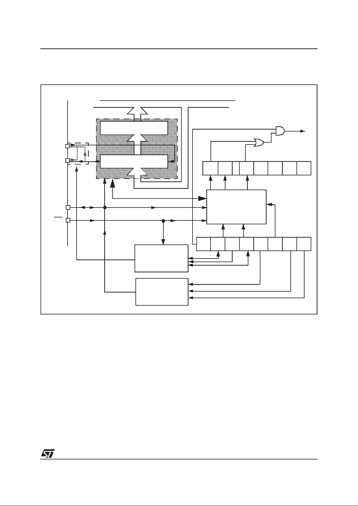
ST72334J/N, ST72314J/N, ST72124J
71/148
SERIAL PERIPHERAL INTERFACE (Cont’d)
Figure 43. Serial Peripheral Interface Block Diagram
DR
Read Buffer
8-Bit Shift Register
Write
Read
Internal Bus
SPI
SPIE SPE SPR2 MSTR CPHA SPR0SPR1CPOL
SPIF
WCOL
MODF
SERIAL
CLOCK
GENERATOR
MOSI
MISO
SS
SCK
CONTROL
STATE
CR
SR
-
--
--
IT
request
MASTER
CONTROL

ST72334J/N, ST72314J/N, ST72124J
72/148
SERIAL PERIPHERAL INTERFACE (Cont’d)
13.4.4 Functional Description
Figure 42 shows the serial peripheral interface
(SPI) block diagram.
This interface contains 3 dedicated registers:
– A Control Register (CR)
– A Status Register (SR)
– A Data Register (DR)
Refer to the CR, SR and DR registers in Section
13.4.7for the bit definitions.
13.4.4.1 Master Configuration
In a masterconfiguration, theserial clockisgenerated on the SCK pin.
Procedure
– Select theSPR0 & SPR1 bits to define the se-
rial clock baud rate (see CR register).
– Select the CPOL and CPHA bits to define one
of the four relationships between the data
transfer and the serial clock (see Figure 45).
– The SSpin must be connected to a high level
signal during the complete byte transmit sequence.
– The MSTRand SPE bits must be set (they re-
main set only if the SS pin is connected to a
high level signal).
In this configuration the MOSI pin is a data output
and to the MISO pin is a data input.
Transmit sequence
The transmit sequencebegins when a byte is written the DR register.
The data byte is parallel loaded into the 8-bit shift
register (from the internal bus) during a write cycle
and then shiftedout serially to the MOSI pin most
significant bit first.
When data transfer is complete:
– The SPIF bit is set by hardware
– An interrupt is generated if the SPIE bit is set
and the I bit in the CCR register is cleared.
During the last clock cycle the SPIF bit is set, a
copy of the data byte received in the shift register
is moved to a buffer. WhentheDR register is read,
the SPI peripheral returns this buffered value.
Clearing the SPIF bit is performed by the following
software sequence:
1.An access to the SR register while the SPIF bit
is set
2.A read to the DR register.
Note: While theSPIF bit is set, all writes to the DR
register are inhibited until the SR register is read.

ST72334J/N, ST72314J/N, ST72124J
73/148
SERIAL PERIPHERAL INTERFACE (Cont’d)
13.4.4.2 Slave Configuration
In slave configuration, the serial clock is received
on the SCK pin from the master device.
The valueof the SPR0& SPR1 bits is not used for
the data transfer.
Procedure
– For correct data transfer, the slave device
must be in the same timing mode as the master device (CPOL and CPHA bits).See Figure
45.
– The SS pin must be connected to a low level
signal during the complete byte transmit sequence.
– Clear the MSTR bit and set the SPE bit to as-
sign the pins to alternate function.
In this configuration the MOSI pin is a data input
and the MISO pin is a data output.
Transmit Sequence
The data byte is parallel loaded into the 8-bit shift
register (from the internal bus) during a write cycle
and then shifted out serially to the MISO pin most
significant bit first.
The transmit sequence begins when the slave device receives the clock signal andthe most significant bit of the data on its MOSI pin.
When data transfer is complete:
– The SPIF bit is set by hardware
– An interrupt is generated if SPIE bit is set and
I bit in CCR register is cleared.
During the last clock cycle the SPIF bit is set, a
copy of the data byte received in the shift register
is moved to a buffer. WhentheDR register is read,
the SPI peripheral returns this buffered value.
Clearing the SPIF bit is performed by the following
software sequence:
1.An access to the SR register while the SPIF bit
is set.
2.A readto the DR register.
Notes: While the SPIF bit is set, all writes to the
DR register are inhibited until the SR register is
read.
The SPIF bit can be cleared during a second
transmission; however, it must be cleared before
the second SPIF bit in order to prevent an overrun
condition (see Section 13.4.4.6).
Depending on the CPHA bit, the SS pin has to be
set to write to the DR register between each data
byte transfer to avoid a write collision (see Section
13.4.4.4).

ST72334J/N, ST72314J/N, ST72124J
74/148
SERIAL PERIPHERAL INTERFACE (Cont’d)
13.4.4.3 Data Transfer Format
During an SPI transfer, data is simultaneously
transmitted (shifted out serially) and received
(shifted in serially). The serial clock is used tosynchronize the data transfer during a sequence of
eight clock pulses.
The SS pin allows individual selection of a slave
device; theother slave devices that are notselected do not interfere with the SPI transfer.
Clock Phase and Clock Polarity
Four possible timing relationships may be chosen
by software, using the CPOL and CPHA bits.
The CPOL (clock polarity) bit controls the steady
state value of the clock when no data is being
transferred. This bit affects both master and slave
modes.
The combination between the CPOL and CPHA
(clock phase) bits selects the data capture clock
edge.
Figure 45, shows an SPI transfer with the four
combinations of the CPHA and CPOL bits. The diagram may be interpreted as a master or slave
timing diagram where the SCK pin, the MISOpin,
the MOSI pin are directly connected between the
master and the slave device.
The SSpin is the slave device selectinput andcan
be driven by the master device.
The master device applies data to its MOSI pinclock edge before the capture clock edge.
CPHA bitis set
The second edge on the SCK pin (falling edge if
the CPOL bit is reset, rising edge if the CPOL bit is
set) is the MSBit capture strobe. Data is latched on
the occurrence of the second clock transition.
No write collision should occur even if the SS pin
stays low during a transfer of several bytes (see
Figure 44).
CPHA bitis reset
The firstedge on the SCK pin (falling edge if CPOL
bit is set, rising edge if CPOL bit is reset) is the
MSBit capture strobe. Data is latched on the occurrence of the first clock transition.
The SS pin must be toggledhigh and low between
each byte transmitted (see Figure 44).
To protect the transmission from a write collision a
low value on the SS pin of a slave device freezes
the data in its DR register and does not allow it to
be altered. Therefore the SS pin must be high to
write a new data byte in the DR without producing
a write collision.
Figure 44. CPHA / SS Timing Diagram
MOSI/MISO
Master
SS
Slave SS
(CPHA=0)
Slave
SS
(CPHA=1)
Byte 1 Byte 2
Byte 3
VR02131A

ST72334J/N, ST72314J/N, ST72124J
75/148
SERIAL PERIPHERAL INTERFACE (Cont’d)
Figure 45. Data Clock Timing Diagram
CPOL = 1)
CPOL = 0)
MISO
(from master)
MOSI
(from slave)
SS
(to slave)
CAPTURE STROBE
CPHA =1
CPOL = 1
CPOL = 0
MSBit Bit 6 Bit 5
Bit 4 Bit3 Bit 2 Bit 1 LSBit
MSBit Bit 6 Bit 5 Bit 4 Bit3 Bit 2 Bit 1 LSBit
MISO
(from master)
MOSI
SS
(to slave)
CAPTURE STROBE
CPHA =0
Note: This figure should not be used as a replacement for parametric information.
Refer to the Electrical Characteristics chapter.
(from slave)
VR02131B
MSBit Bit 6 Bit 5
Bit 4 Bit3 Bit 2 Bit 1 LSBit
MSBit Bit 6 Bit 5
Bit 4 Bit3 Bit 2 Bit 1 LSBit
SCLK (with
SCLK (with

ST72334J/N, ST72314J/N, ST72124J
76/148
SERIAL PERIPHERAL INTERFACE (Cont’d)
13.4.4.4 Write Collision Error
A write collision occurs when the software tries to
write tothe DR register while a data transfer is taking place with an external device. When this happens, the transfer continues uninterrupted; and
the software write will be unsuccessful.
Write collisionscan occur both inmaster andslave
mode.
Note: a ”read collision” will never occur since the
received data byte is placed in a buffer in which
access is alwayssynchronous with the MCU operation.
In Slave mode
When the CPHA bit is set:
The slave device will receive a clock (SCK) edge
prior to the latch of the first data transfer. This first
clock edge will freeze the data in the slave device
DR register and output the MSBit on to the external MISO pin of the slave device.
The SS pin low state enables the slave device but
the output of the MSBit onto the MISO pin does
not take place until the first data transfer clock
edge.
When the CPHA bit is reset:
Data is latched on the occurrence of the first clock
transition. The slave device does not have any
way of knowing when that transition will occur;
therefore, the slave device collision occurs when
software attempts to write the DR register after its
SS pin has been pulled low.
For this reason, the SS pin mustbe high, between
each data byte transfer, to allow the CPU to write
in the DR register without generating a write collision.
In Master mode
Collision in the master device is defined as a write
of the DR register while the internal serial clock
(SCK) is in the process of transfer.
The SS pin signal must be always high on the
master device.
WCOL bit
The WCOL bit in the SR register is set if a write
collision occurs.
No SPI interrupt is generated when the WCOL bit
is set (the WCOL bit is a status flag only).
Clearing the WCOL bit is done through a software
sequence (see Figure 46).
Figure 46. Clearing the WCOL bit (Write Collision Flag) Software Sequence
Clearing sequence after SPIF = 1 (end of a data byte transfer)
1st Step
Read SR
Read DR Write DR
2nd Step
SPIF =0
WCOL=0
SPIF =0
WCOL=0 if no transfer has started
WCOL=1 if a transfer has started
Clearing sequence before SPIF = 1 (during a data byte transfer)
1st Step
2nd Step
WCOL=0
before the 2nd step
Read SR
Read DR
Note: Writing in DR register instead of reading in it do not reset
WCOL bit
Read SR
OR
THEN
THEN
THEN

ST72334J/N, ST72314J/N, ST72124J
77/148
SERIAL PERIPHERAL INTERFACE (Cont’d)
13.4.4.5 Master Mode Fault
Master mode fault occurs when the master device
has itsSS pin pulled low, then the MODF bit isset.
Master modefault affects theSPI peripheral in the
following ways:
– The MODF bit is set and an SPI interrupt is
generated if the SPIE bit is set.
– The SPE bit is reset. This blocks all output
from the device and disables the SPI peripheral.
– The MSTR bit is reset, thus forcing the device
into slave mode.
Clearing the MODF bit is done through a software
sequence:
1. A read or write access to the SR register while
the MODF bit is set.
2. A write to the CR register.
Notes: To avoid any multiple slave conflicts in the
case of a system comprising several MCUs, the
SS pin must be pulled high during the clearing sequence of the MODF bit. The SPE and MSTR bits
may be restored to their original state during or after this clearing sequence.
Hardware does not allow the user to set the SPE
and MSTR bits while the MODFbit is set except in
the MODF bit clearing sequence.
In a slave device the MODF bit can not be set, but
in a multi master configuration the device canbe in
slave mode with this MODF bit set.
The MODF bit indicates that there might have
been amulti-master conflict for system control and
allows a proper exit from system operation to a reset or default system state using an interrupt routine.
13.4.4.6 Overrun Condition
An overrun condition occurs when the master device has sent several data bytes and the slavedevice has not cleared the SPIF bit issuing from the
previous data byte transmitted.
In this case, the receiver buffer contains the byte
sent after the SPIF bit was last cleared. A read to
the DR register returns this byte. All other bytes
are lost.
This condition is not detected by the SPI peripheral.
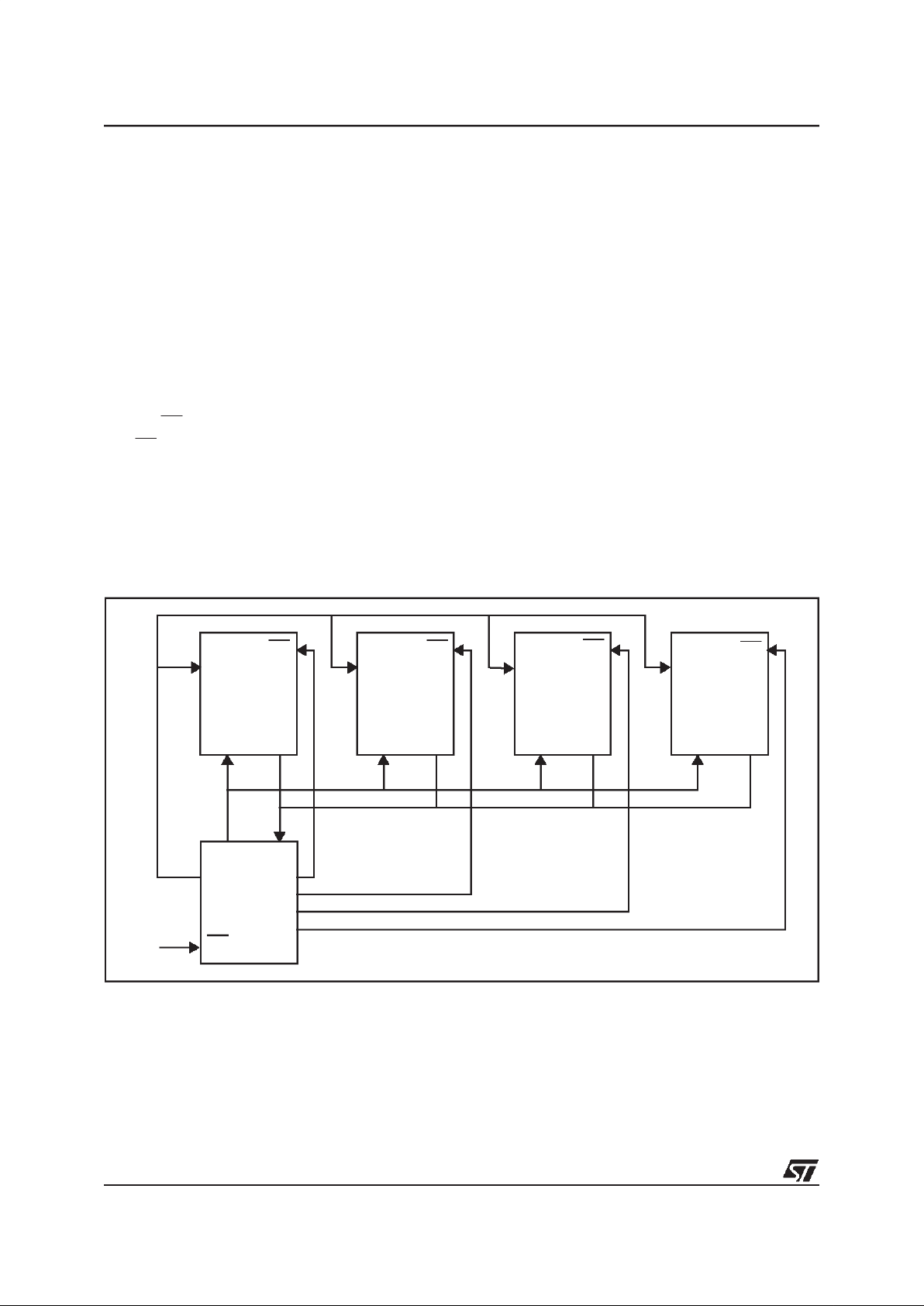
ST72334J/N, ST72314J/N, ST72124J
78/148
SERIAL PERIPHERAL INTERFACE (Cont’d)
13.4.4.7 Single Master and Multimaster Configurations
There are two types of SPI systems:
– Single Master System
– Multimaster System
Single Master System
A typical single master systemmay be configured,
using an MCU as the master and four MCUs as
slaves (see Figure 47).
The master device selects the individual slave devices byusing four pins of a parallel port to control
the four SS pins of the slave devices.
The SS pinsare pulled high during reset since the
master device ports will be forced to be inputs at
that time, thus disabling the slave devices.
Note: To prevent a bus conflict on the MISO line
the master allows only one active slave device
during a transmission.
For more security, the slave device may respond
to the master with the received data byte. Then the
master will receive the previous byte backfrom the
slave device if all MISO and MOSI pins are connected and the slave has not written its DR register.
Other transmission security methods can use
ports for handshake lines or data bytes with command fields.
Multi-master System
A multi-master system may also be configured by
the user. Transfer of master control could be implemented using a handshake methodthrough the
I/O ports or by an exchange of code messages
through the serial peripheral interface system.
The multi-master system is principally handled by
the MSTR bit in the CR register and the MODF bit
in the SR register.
Figure 47. Single Master Configuration
MISO
MOSI
MOSI
MOSI MOSI MOSIMISO MISO MISOMISO
SS
SS
SS
SS
SS
SCK SCK
SCK
SCK
SCK
5V
Ports
Slave
MCU
Slave
MCU
Slave
MCU
Slave
MCU
Master
MCU
ST72334J/N, ST72314J/N, ST72124J
79/148
SERIAL PERIPHERAL INTERFACE (Cont’d)
13.4.5 Low Power Modes
13.4.6 Interrupts
Note: The SPI interrupt events are connected to
the sameinterrupt vector(see Interrupts chapter).
They generate an interrupt if the corresponding
Enable Control Bitis set and the interrupt mask in
the CC register is reset (RIM instruction).
Mode Description
WAIT
No effect on SPI.
SPI interrupt events cause the device to exit fromWAIT mode.
HALT
SPI registers are frozen.
In HALT mode, the SPI is inactive. SPI operation resumes when the MCU is woken up by an interrupt with
“exit from HALT mode” capability.
Interrupt Event
Event
Flag
Enable
Control
Bit
Exit
from
Wait
Exit
from
Halt
SPI End of Transfer Event SPIF
SPIE
Yes No
Master Mode Fault Event MODF Yes No

ST72334J/N, ST72314J/N, ST72124J
80/148
SERIAL PERIPHERAL INTERFACE (Cont’d)
13.4.7 Register Description
CONTROL REGISTER (CR)
Read/Write
Reset Value: 0000xxxx (0xh)
Bit 7 = SPIE
Serial peripheral interrupt enable.
This bit is set and cleared bysoftware.
0: Interrupt is inhibited
1: An SPI interrupt is generated whenever SPIF=1
or MODF=1 in the SR register
Bit 6 = SPE
Serial peripheral output enable.
This bit is set and cleared by software. It is also
cleared by hardware when, inmaster mode, SS=0
(see Section 13.4.4.5 ”Master Mode Fault” on
page 77).
0: I/O port connected to pins
1: SPI alternate functions connected to pins
The SPEbit is cleared by reset, so the SPI peripheral is not initially connected to the external pins.
Bit 5 = SPR2
Divider Enable
.
this bit is set and cleared by software and it is
cleared by reset. It is usedwith the SPR[1:0] bits to
set the baud rate. Refer to Table 17.
0: Divider by 2 enabled
1: Divider by 2 disabled
Bit 4 = MSTR
Master.
This bit is set and cleared by software. It is also
cleared by hardware when, inmaster mode, SS=0
(see Section 13.4.4.5 ”Master Mode Fault” on
page 77).
0: Slave mode is selected
1: Master mode is selected, the function of the
SCK pin changes from an input to an output and
the functions of the MISO and MOSI pinsare reversed.
Bit 3 = CPOL
Clock polarity.
This bit is set and cleared by software. This bit determines the steady state of the serial Clock. The
CPOL bit affects both the master and slave
modes.
0: The steady state is a low value at the SCK pin.
1: The steady stateis a high value at the SCK pin.
Bit 2 = CPHA
Clock phase.
This bit is set andcleared by software.
0: The first clock transition is the first data capture
edge.
1: The second clock transition is the first capture
edge.
Bit 1:0 = SPR[1:0]
Serial peripheral rate.
These bits are set and cleared by software.Used
with the SPR2 bit, they select one of six baud rates
to be used as the serial clock when the device is a
master.
These 2 bits have no effect in slave mode.
Table 17. Serial Peripheral Baud Rate
70
SPIE SPE SPR2 MSTR CPOL CPHA SPR1 SPR0
Serial Clock SPR2 SPR1 SPR0
f
CPU
/2 1 0 0
f
CPU
/8 0 0 0
f
CPU
/16 0 0 1
f
CPU
/32 1 1 0
f
CPU
/64 0 1 0
f
CPU
/128 0 1 1

ST72334J/N, ST72314J/N, ST72124J
81/148
SERIAL PERIPHERAL INTERFACE (Cont’d)
STATUS REGISTER (SR)
Read Only
Reset Value: 0000 0000 (00h)
Bit 7 = SPIF
Serial Peripheraldata transfer flag.
This bit is set by hardware when a transfer has
been completed. An interrupt is generated if
SPIE=1 in the CR register. It is cleared by a software sequence (an access to the SR register followed by a read or write to the DR register).
0: Data transfer is in progress or has been ap-
proved by a clearing sequence.
1: Data transfer between thedevice and an exter-
nal device has been completed.
Note: Whilethe SPIF bit isset, all writes to the DR
register are inhibited.
Bit 6 = WCOL
Write Collision status.
This bit is set by hardware when a write to the DR
register is done during a transmit sequence. It is
cleared by a software sequence (see Figure 46).
0: No write collision occurred
1: A write collision has been detected
Bit 5 = Unused.
Bit 4 = MODF
Mode Fault flag.
This bit is set by hardware when the SS pin is
pulled low in master mode (see Section 13.4.4.5
”Master ModeFault” onpage77). An SPIinterrupt
can be generated if SPIE=1 in the CR register.
This bit is cleared by a software sequence(An access to the SR register while MODF=1followedby
a write to the CR register).
0: No master mode fault detected
1: A fault in master mode has been detected
Bits 3-0 = Unused.
DATA I/O REGISTER (DR)
Read/Write
Reset Value: Undefined
The DR register is used to transmit and receive
data on the serialbus. In the master device only a
write to this register will initiate transmission/reception of another byte.
Notes: During the last clock cycle the SPIF bit is
set, a copy of the received data byte in the shift
register is moved to a buffer. When the user reads
the serialperipheral data I/O register, the buffer is
actually being read.
Warning:
A write to the DR register places data directly into
the shift register fortransmission.
A write to the the DR register returns the value located inthe bufferand notthe contents of the shift
register (See Figure 43 ).
70
SPIF WCOL - MODF - - - -
70
D7 D6 D5 D4 D3 D2 D1 D0

ST72334J/N, ST72314J/N, ST72124J
82/148
SERIAL PERIPHERAL INTERFACE (Cont’d)
Table 18. SPI Register Map and Reset Values
Address
(Hex.)
Register
Label
76543210
0021h
SPIDR
Reset Value
MSB
xxxxxxx
LSB
x
0022h
SPICR
Reset Value
SPIE
0
SPE
0
SPR20MSTR0CPOL
x
CPHA
x
SPR1
x
SPR0
x
0023h
SPISR
Reset Value
SPIF
0
WCOL
00
MODF
00000

ST72334J/N, ST72314J/N, ST72124J
83/148
13.5 SERIAL COMMUNICATIONS INTERFACE (SCI)
13.5.1 Introduction
The Serial Communications Interface (SCI) offers
a flexible means of full-duplex data exchange with
external equipment requiring an industry standard
NRZ asynchronous serialdata format.The SCI offers a very wide range of baud rates using two
baud rate generator systems.
13.5.2 Main Features
■ Full duplex, asynchronous communications
■ NRZ standard format (Mark/Space)
■ Dual baud rate generator systems
■ Independently programmable transmit and
receive baud rates up to 250K baud.
■ Programmable data word length (8 or 9 bits)
■ Receive buffer full, Transmit buffer empty and
End of Transmission flags
■ Two receiver wake-up modes:
– Address bit (MSB)
– Idle line
■ Mutingfunctionformultiprocessorconfigurations
■ Separate enable bits for Transmitter and
Receiver
■ Three error detection flags:
– Overrun error
– Noise error
– Frame error
■ Five interrupt sources with flags:
– Transmit data register empty
– Transmission complete
– Receive data register full
– Idle line received
– Overrun error detected
13.5.3 General Description
The interface is externally connected to another
device by two pins (see Figure 49):
– TDO: TransmitData Output.When the transmit-
ter is disabled, the output pin returns to its I/O
port configuration. When the transmitter is enabled and nothing is to be transmitted, the TDO
pin is at high level.
– RDI: Receive Data Input is the serial data input.
Oversampling techniques are used for data recovery by discriminating between valid incoming
data and noise.
Through this pins, serialdata is transmittedand received as frames comprising:
– An Idle Line prior to transmission or reception
– A start bit
– A data word (8 or 9 bits) least significant bit first
– A Stop bit indicating that the frame is complete.
Thisinterfaceusestwotypesofbaudrategenerator:
– A conventional type for commonly-used baud
rates,
– An extended typewitha prescaler offeringa very
wide rangeofbaudrates even withnon-standard
oscillator frequencies.

ST72334J/N, ST72314J/N, ST72124J
84/148
SERIAL COMMUNICATIONS INTERFACE (Cont’d)
Figure 48. SCI Block Diagram
WAKE
UP
UNIT
RECEIVER
CONTROL
SR
TRANSMIT
CONTROL
TDRE TC RDRF
IDLE OR NF FE -
SCI
CONTROL
INTERRUPT
CR1
R8
T8
-
M
WAKE
-
--
Received Data Register (RDR)
Received Shift Register
Read
Transmit Data Register (TDR)
Transmit Shift Register
Write
RDI
TDO
(DATA REGISTER)DR
TRANSMITTER
CLOCK
RECEIVER
CLOCK
RECEIVER RATE
TRANSMITTER RATE
BRR
SCP1
f
CPU
CONTROL
CONTROL
SCP0SCT2 SCT1 SCT0SCR2SCR1SCR0
/2 /PR
/16
CONVENTIONAL BAUD RATE GENERATOR
SBKRWURETEILIERIETCIETIE
CR2

ST72334J/N, ST72314J/N, ST72124J
85/148
SERIAL COMMUNICATIONS INTERFACE (Cont’d)
13.5.4 Functional Description
The block diagram of the Serial Control Interface,
is shown in Figure 48. It contains 6 dedicated registers:
– Two control registers (CR1 & CR2)
– A status register (SR)
– A baud rate register (BRR)
– An extended prescaler receiver register (ERPR)
– Anextendedprescalertransmitterregister (ETPR)
Refer to the register descriptions in Section
13.5.7for the definitions of each bit.
13.5.4.1 Serial Data Format
Word lengthmay be selected as being either 8or 9
bits by programming the M bit in the CR1 register
(see Figure 48).
The TDOpin is in low state during the start bit.
The TDOpin is in high state during the stop bit.
An Idle character is interpreted as an entire frame
of “1”s followed by the start bit of the next frame
which contains data.
A Break character is interpreted on receiving “0”s
for some multiple of theframe period.At the end of
the last break frame the transmitter inserts an extra “1” bit to acknowledge the start bit.
Transmission and reception are driven by their
own baud rate generator.
Figure 49. Word length programming
Bit0 Bit1
Bit2
Bit3 Bit4 Bit5 Bit6 Bit7 Bit8
Start
Bit
Stop
Bit
Next
Start
Bit
Idle Frame
Bit0 Bit1
Bit2
Bit3 Bit4
Bit5 Bit6
Bit7
Start
Bit
Stop
Bit
Next
Start
Bit
Start
Bit
Idle Frame
Start
Bit
9-bit Word length (M bit is set)
8-bit Word length (M bit is reset)
Possible
Parity
Bit
Possible
Parity
Bit
Break Frame
Start
Bit
Extra
’1’
Data Frame
Break Frame
Start
Bit
Extra
’1’
Data Frame
Next Data Frame
Next Data Frame

ST72334J/N, ST72314J/N, ST72124J
86/148
SERIAL COMMUNICATIONS INTERFACE (Cont’d)
13.5.4.2 Transmitter
The transmitter can send data words of either 8 or
9 bits depending on the M bit status. When the M
bit is set, word length is 9 bits and the 9th bit (the
MSB) hasto be stored in the T8 bit in the CR1 register.
Character Transmission
During an SCI transmission, data shifts out least
significant bit first on the TDO pin. In this mode,
the DRregister consists of abuffer (TDR) between
the internal bus and the transmit shift register (see
Figure 48).
Procedure
– Select the M bit to define the word length.
– Select the desiredbaud rate using theBRR and
the ETPR registers.
– Set the TE bit to assign the TDO pinto the alter-
nate function and to send a idle frame as first
transmission.
– Access the SR register and write the data to
send in theDR register (thissequence clears the
TDRE bit).Repeat thissequencefor each datato
be transmitted.
Clearing the TDRE bit is always performed by the
following software sequence:
1. An access to the SR register
2. A write to the DR register
The TDRE bit is set by hardware and it indicates:
– The TDR register is empty.
– The data transfer is beginning.
– The next data can be written in the DR register
without overwriting the previous data.
This flag generates an interruptif the TIE bit is set
and the I bit is cleared in the CCR register.
When a transmission is taking place, a write instruction to the DR register stores the data in the
TDR register and which is copied in the shift register at the end of the current transmission.
When no transmission is taking place, a write instruction tothe DRregister places the data directly
in the shift register, the data transmission starts,
and the TDRE bit is immediately set.
When a frame transmission is complete (after the
stop bit or after the break frame) the TC bit is set
and an interrupt is generated if theTCIE is set and
the I bit is cleared in the CCR register.
Clearing the TC bit is performed by the following
software sequence:
1. An access to the SR register
2. A write to the DR register
Note: The TDRE and TC bits are cleared by the
same software sequence.
Break Characters
Setting the SBK bit loads the shift register with a
break character. The break frame length depends
on the M bit (see Figure 49).
As long as the SBK bit is set, the SCI send break
frames to the TDO pin. After clearing this bit by
software the SCI insert a logic 1 bit at the end of
the last break frame to guarantee the recognition
of the start bit of the next frame.
Idle Characters
Setting the TE bit drives the SCI to send an idle
frame before the first data frame.
Clearing and then settingthe TE bit during a transmission sends an idle frame after thecurrent word.
Note: Resetting and setting the TE bit causes the
data in the TDR register to be lost. Therefore the
best time to toggle the TE bit is when the TDRE bit
is set i.e. before writing the next byte inthe DR.

ST72334J/N, ST72314J/N, ST72124J
87/148
SERIAL COMMUNICATIONS INTERFACE (Cont’d)
13.5.4.3 Receiver
The SCI can receive data words of either 8 or 9
bits. When the M bit is set, word length is 9 bits
and the MSB isstored in the R8 bit in the CR1 register.
Character reception
During a SCI reception, data shifts in least significant bit first through the RDI pin. In this mode, DR
register consists in a buffer (RDR) between the internal bus and the received shift register (see Figure 48).
Procedure
– Select the M bit to define the word length.
– Select the desiredbaud rate using theBRR and
the ERPR registers.
– Set the RE bit, this enables the receiver which
begins searching for a start bit.
When a character is received:
– The RDRF bit is set. It indicates that the content
of the shift register is transferred to the RDR.
– An interrupt is generated if the RIE bit is set and
the I bit is cleared in the CCR register.
– The error flags can be set if a frame error, noise
or anoverrun errorhas been detected during re-
ception.
Clearing theRDRF bit isperformed by thefollowing
software sequence done by:
1. An access to the SR register
2. A read to the DR register.
The RDRFbit mustbe cleared beforetheendofthe
reception of the next character to avoid anoverrun
error.
Break Character
When a break character is received, the SPI handles it as a framing error.
Idle Character
When a idle frame is detected, there is the same
procedure as a data received character plus an interrupt if theILIE bit is set and the I bit is cleared in
the CCR register.
Overrun Error
An overrun error occurs when a character is received when RDRF has not been reset. Data can
not be transferred from the shift register to the
TDR register as long as the RDRF bit is not
cleared.
When a overrun error occurs:
– The OR bit is set.
– The RDR content will not be lost.
– The shift register will be overwritten.
– Aninterrupt is generated ifthe RIE bitis set and
the I bit is cleared in the CCR register.
The OR bit is reset by an access to theSR register
followed by a DR register read operation.
Noise Error
Oversampling techniques are used for data recovery by discriminating between valid incoming data
and noise.
When noise is detected in a frame:
– The NF is set at the rising edge of the RDRF bit.
– Data is transferred from the Shiftregister to the
DR register.
– No interrupt is generated. However this bit rises
at the same time as the RDRF bit which itself
generates an interrupt.
The NF bitis reset by a SR register read operation
followed by a DR register read operation.
Framing Error
A framing error is detected when:
– Thestop bit is not recognized on receptionat the
expected time, following either a de-synchroni-
zation or excessive noise.
– A break is received.
When the framing error is detected:
– the FE bit is set by hardware
– Data is transferred from the Shiftregister to the
DR register.
– No interrupt is generated. However this bit rises
at the same time as the RDRF bit which itself
generates an interrupt.
The FE bit is reset by a SR register read operation
followed by a DR register read operation.

ST72334J/N, ST72314J/N, ST72124J
88/148
SERIAL COMMUNICATIONS INTERFACE (Cont’d)
Figure 50. SCI Baud Rate and Extended Prescaler Block Diagram
TRANSMITTER
RECEIVER
ETPR
ERPR
EXTENDED PRESCALER RECEIVER RATE CONTROL
EXTENDED PRESCALER TRANSMITTERRATE CONTROL
EXTENDED PRESCALER
CLOCK
CLOCK
RECEIVER RATE
TRANSMITTER RATE
BRR
SCP1
f
CPU
CONTROL
CONTROL
SCP0SCT2 SCT1 SCT0SCR2SCR1SCR0
/2 /PR
/16
CONVENTIONAL BAUD RATE GENERATOR
EXTENDEDRECEIVER PRESCALER REGISTER
EXTENDEDTRANSMITTER PRESCALERREGISTER

ST72334J/N, ST72314J/N, ST72124J
89/148
SERIAL COMMUNICATIONS INTERFACE (Cont’d)
13.5.4.4 Conventional Baud Rate Generation
The baud rate for the receiver and transmitter (Rx
and Tx) are set independently and calculated as
follows:
with:
PR = 1, 3, 4 or 13 (see SCP0 & SCP1 bits)
TR = 1, 2, 4, 8, 16, 32, 64,128
(see SCT0, SCT1 & SCT2 bits)
RR = 1, 2, 4, 8, 16, 32, 64,128
(see SCR0,SCR1 & SCR2 bits)
All this bits are in the BRR register.
Example: If f
CPU
is 8 MHz (normal mode) and if
PR=13 and TR=RR=1, the transmit and receive
baud rates are 19200 baud.
Note: the baud rate registers MUST NOT be
changed while the transmitter or the receiverisenabled.
13.5.4.5 Extended Baud Rate Generation
The extended prescaler option gives a very fine
tuning onthe baud rate, using a 255 value prescaler, whereas the conventional Baud Rate Generator retains industry standard software compatibility.
The extended baud rate generator block diagram
is described in the Figure 50.
The output clock rate sent to the transmitter or to
the receiver will be the output from the 16 divider
divided bya factor ranging from 1 to 255 set in the
ERPR or theETPR register.
Note: the extended prescaler is activated by setting the ETPR or ERPR register to a value other
than zero. The baud rates are calculated as follows:
with:
ETPR = 1,..,255 (see ETPR register)
ERPR = 1,.. 255 (see ERPR register)
13.5.4.6 Receiver Muting andWake-up Feature
In multiprocessor configurations it is often desirable that only the intended message recipient
should actively receive the full message contents,
thus reducing redundant SCI service overhead for
all non addressed receivers.
The non addressed devices may be placed in
sleep mode by means of the muting function.
Setting the RWU bit by software puts the SCI in
sleep mode:
All the reception status bits can not be set.
All the receive interrupt are inhibited.
A mutedreceiver may be awakened by one of the
following two ways:
– by Idle Line detection if the WAKE bit is reset,
– by AddressMark detectionif the WAKEbitisset.
Receiver wakes-up by Idle Line detection when
the Receive line has recognised an Idle Frame.
Then the RWU bit is reset by hardware but the
IDLE bit is not set.
Receiver wakes-up by Address Mark detection
when it received a “1” as the most significant bit of
a word, thus indicating thatthe message is an address. The reception of this particular word wakes
up the receiver, resets the RWU bit and sets the
RDRF bit, which allows thereceiver to receive this
word normally and to use it as an addressword.
Tx =
(32*PR)*TR
f
CPU
Rx =
(32*PR)*RR
f
CPU
Tx =
16*ETPR
f
CPU
Rx =
16*ERPR
f
CPU

ST72334J/N, ST72314J/N, ST72124J
90/148
SERIAL COMMUNICATIONS INTERFACE (Cont’d)
13.5.5 Low Power Modes
13.5.6 Interrupts
The SCI interrupt events are connected to the
same interrupt vector (see Interrupts chapter).
These events generate an interrupt if the corresponding Enable Control Bit is set and the interrupt mask in the CC register is reset (RIMinstruction).
Mode Description
WAIT
No effect on SCI.
SCI interrupts cause the device to exitfrom Wait mode.
HALT
SCI registers are frozen.
In Halt mode, the SCI stops transmitting/receiving until Halt mode is exited.
Interrupt Event
Event
Flag
Enable
Control
Bit
Exit
from
Wait
Exit
from
Halt
Transmit Data Register Empty TDRE TIE Yes No
Transmission Complete TC TCIE Yes No
Received Data Ready to be Read RDRF
RIE
Yes No
Overrrun Error Detected OR Yes No
Idle Line Detected IDLE ILIE Yes No

ST72334J/N, ST72314J/N, ST72124J
91/148
SERIAL COMMUNICATIONS INTERFACE (Cont’d)
13.5.7 Register Description
STATUS REGISTER (SR)
Read Only
Reset Value: 1100 0000 (C0h)
Bit 7 = TDRE
Transmit data register empty.
This bit is set by hardware when the content of the
TDR register has been transferred into the shift
register. An interrupt is generated if the TIE =1 in
the CR2 register. It is cleared by a software sequence (an access to the SR register followed by a
write to the DR register).
0: Data is not transferred to the shift register
1: Data is transferred to the shift register
Note: data will not be transferred to the shift register as long as the TDRE bit is not reset.
Bit 6 = TC
Transmission complete.
This bit is set by hardware when transmission of a
frame containing Data, a Preamble or a Break is
complete. An interrupt is generated if TCIE=1 in
the CR2 register. It is cleared by a software sequence (an access to the SR register followed by a
write to the DR register).
0: Transmission is not complete
1: Transmission is complete
Bit 5 = RDRF
Received data ready flag.
This bit is set by hardware when the content of the
RDR register has been transferred into the DR
register. An interrupt is generated if RIE=1 in the
CR2 register. It is cleared by hardware when
RE=0 orbya software sequence (an access to the
SR register followed by a readto the DR register).
0: Data is not received
1: Received data is ready to be read
Bit 4 = IDLE
Idle line detect.
This bit is set by hardware when a Idle Line is detected. An interrupt is generated if the ILIE=1 in
the CR2 register. It is cleared by hardware when
RE=0 by a software sequence (an access to the
SR register followed by a readto the DR register).
0: No Idle Line is detected
1: Idle Lineis detected
Note: The IDLE bit will not be set again until the
RDRF bit has been set itself (i.e. a new idle line occurs). This bit isnotset by an idle line whenthe receiver wakes up from wake-up mode.
Bit 3 = OR
Overrun error.
This bit is set by hardware whenthe wordcurrently
being received in the shift register is ready to be
transferred into the RDR register while RDRF=1.
An interrupt is generated if RIE=1 in the CR2 register. It is cleared by hardware when RE=0 by a
software sequence (an access to the SR register
followed by a read to the DR register).
0: No Overrun error
1: Overrun error is detected
Note: When this bit is set RDR register content will
not be lost but the shift register will be overwritten.
Bit 2 = NF
Noise flag.
This bit is set by hardware when noise is detected
on a received frame. It is cleared by hardware
when RE=0 by a software sequence (an access to
the SR register followed bya read to the DR register).
0: No noise is detected
1: Noise is detected
Note: This bit does not generate interrupt as it appears at the same time as the RDRF bit which itself generates an interrupt.
Bit 1 = FE
Framing error.
This bit isset by hardware whena de-synchronization, excessive noise or a break character is detected. It is cleared by hardware when RE=0 by a
software sequence (an access to the SR register
followed by a read to the DR register).
0: No Framing error is detected
1: Framing error or break character is detected
Note: This bit does not generate interrupt as it appears at the same time as the RDRF bit which itself generates an interrupt. If the word currently
being transferred causes both frame error and
overrun error, it will be transferred and only theOR
bit will be set.
Bit 0 = Unused.
70
TDRE TC RDRF IDLE OR NF FE -

ST72334J/N, ST72314J/N, ST72124J
92/148
SERIAL COMMUNICATIONS INTERFACE (Cont’d)
CONTROL REGISTER 1 (CR1)
Read/Write
Reset Value: Undefined
Bit 7 = R8
Receive data bit 8.
This bit is used to store the 9th bit of the received
word when M=1.
Bit 6 = T8
Transmit data bit 8.
This bit is used to store the 9th bit of the transmitted word when M=1.
Bit 4 = M
Word length.
This bit determines the word length. It is set or
cleared by software.
0: 1 Start bit, 8 Data bits, 1 Stop bit
1: 1 Start bit, 9 Data bits, 1 Stop bit
Bit 3 = WAKE
Wake-Up method.
This bit determines the SCI Wake-Up method, it is
set or cleared by software.
0: Idle Line
1: Address Mark
CONTROL REGISTER 2 (CR2)
Read/Write
Reset Value: 0000 0000 (00h)
Bit 7 = TIE
Transmitter interrupt enable
.
This bit is set and cleared bysoftware.
0: interrupt is inhibited
1: An SCI interrupt is generated whenever
TDRE=1 in the SR register.
Bit 6 = TCIE
Transmission complete interrupt ena-
ble
This bit is set and cleared bysoftware.
0: interrupt is inhibited
1: AnSCI interruptis generated whenever TC=1 in
the SR register
Bit 5 = RIE
Receiver interrupt enable
.
This bit is set andcleared by software.
0: interrupt is inhibited
1: An SCI interrupt is generated whenever OR=1
or RDRF=1 in the SR register
Bit 4 = ILIE
Idle line interrupt enable.
This bit is set andcleared by software.
0: interrupt is inhibited
1: An SCIinterrupt is generated whenever IDLE=1
in the SR register.
Bit 3 = TE
Transmitter enable.
This bit enables the transmitter and assigns the
TDO pin to the alternate function. It is set and
cleared by software.
0: Transmitter is disabled, the TDO pin is back to
the I/O port configuration.
1: Transmitter is enabled
Note: during transmission, a “0” pulse on the TE
bit (“0” followed by “1”) sends a preamble after the
current word.
Bit 2 = RE
Receiver enable.
This bit enables the receiver. It is set and cleared
by software.
0: Receiver is disabled, it resets the RDRF, IDLE,
OR, NF and FE bits of theSR register.
1: Receiver is enabled and begins searching for a
start bit.
Bit 1 = RWU
Receiver wake-up.
This bit determines if the SCI is in mute mode or
not. It is set and cleared by software and can be
cleared by hardware when a wake-up sequence is
recognized.
0: Receiver in active mode
1: Receiver in mute mode
Bit 0 = SBK
Send break.
This bit set is used to send break characters. It is
set and cleared by software.
0: No break character is transmitted
1: Break characters are transmitted
Note: If the SBK bit issetto “1”and thento“0”, the
transmitter will send a BREAK word at the end of
the current word.
70
R8 T8 - M WAKE - -
-
70
TIE TCIE RIE ILIE TE RE RWU
SBK

ST72334J/N, ST72314J/N, ST72124J
93/148
SERIAL COMMUNICATIONS INTERFACE (Cont’d)
DATA REGISTER (DR)
Read/Write
Reset Value: Undefined
Contains the Received or Transmitted data char-
acter, depending onwhether it is read from or written to.
The Data register performs a double function (read
and write) since it is composed of two registers,
one for transmission (TDR) and one for reception
(RDR).
The TDR register provides the parallel interface
between the internal bus and the output shift register (see Figure 48).
The RDR register provides the parallel interface
between the input shift register and the internal
bus (see Figure48).
BAUD RATE REGISTER (BRR)
Read/Write
Reset Value: 00xx xxxx (XXh)
Bit 7:6= SCP[1:0]
First SCI Prescaler
These 2 prescaling bits allow several standard
clock division ranges:
Bit 5:3 = SCT[2:0]
SCI Transmitter rate divisor
These 3 bits, in conjunction with the SCP1& SCP0
bits define the total division applied to the bus
clock to yield thetransmit rate clock inconventional Baud Rate Generator mode.
Note: this TR factor is used only when the ETPR
fine tuning factor is equal to 00h; otherwise, TR is
replaced by the ETPR dividing factor.
Bit 2:0 = SCR[2:0]
SCI Receiver rate divisor.
These 3 bits, in conjunction with the SCP1& SCP0
bits define the total division applied to the bus
clock to yield thereceive rate clock in conventional
Baud Rate Generator mode.
Note: this RR factor is used only when the ERPR
fine tuningfactor is equal to 00h; otherwise, RR is
replaced by the ERPR dividing factor.
70
DR7 DR6 DR5 DR4 DR3 DR2 DR1 DR0
70
SCP1 SCP0 SCT2 SCT1 SCT0 SCR2 SCR1 SCR0
PR Prescaling factor SCP1 SCP0
100
301
410
13 1 1
TR dividingfactor SCT2 SCT1 SCT0
1 000
2 001
4 010
8 011
16 100
32 101
64 110
128 1 1 1
RR dividingfactor SCR2 SCR1 SCR0
1 000
2 001
4 010
8 011
16 100
32 101
64 110
128 1 1 1

ST72334J/N, ST72314J/N, ST72124J
94/148
SERIAL COMMUNICATIONS INTERFACE (Cont’d)
EXTENDED RECEIVE PRESCALER DIVISION
REGISTER (ERPR)
Read/Write
Reset Value: 0000 0000 (00h)
Allows setting of the Extended Prescaler rate divi-
sion factor for the receive circuit.
Bit 7:1 = ERPR[7:0]
8-bit Extended ReceivePres-
caler Register.
The extended Baud Rate Generator is activated
when a value different from 00h is stored in this
register. Therefore the clock frequency issued
from the 16 divider (see Figure 50) is divided by
the binary factor set in the ERPR register (in the
range 1 to 255).
The extended baud rate generator is not used after a reset.
EXTENDED TRANSMIT PRESCALER DIVISION
REGISTER (ETPR)
Read/Write
Reset Value:0000 0000 (00h)
Allows setting of the External Prescaler rate divi-
sion factor for the transmit circuit.
Bit 7:1 = ETPR[7:0]
8-bit ExtendedTransmitPres-
caler Register.
The extended Baud Rate Generator is activated
when a value different from 00h is stored in this
register. Therefore the clock frequency issued
from the 16 divider (see Figure 50) is divided by
the binary factor set in the ETPR register (in the
range 1 to 255).
The extended baud rate generator is not used after a reset.
Table 19. SCI Register Map and Reset Values
70
ERPR7ERPR6ERPR5ERPR4ERPR3ERPR2ERPR1ERPR
0
70
ETPR7ETPR6ETPR5ETPR4ETPR3ETPR2ETPR1ETPR
0
Address
(Hex.)
Register
Label
76543210
0050h
SCISR
Reset Value
TDRE
1
TC
1
RDRF
0
IDLE
0
OR
0
NF
0
FE
00
0051h
SCIDR
Reset Value
MSB
xxxxxxx
LSB
x
0052h
SCIBRR
Reset Value
SOG
00
VPOLx2FHDETxHVSELxVCORDISxCLPINVxBLKINV
x
0053h
SCICR1
Reset Value
R8
x
T8
x0
M
x
WAKE
x000
0054h
SCICR2
Reset Value
TIE
0
TCIE
0
RIE
0
ILIE
0
TE
0
RE
0
RWU
0
SBK
0
0055h
SCIPBRR
Reset Value
MSB
0000000
LSB
0
0057h
SCIPBRT
Reset Value
MSB
0000000
LSB
0

ST72334J/N, ST72314J/N, ST72124J
95/148
13.6 8-BIT A/D CONVERTER (ADC)
13.6.1 Introduction
The on-chipAnalogto Digital Converter (ADC) peripheral is a 8-bit, successive approximation converter with internal sample and hold circuitry. This
peripheral has up to 16 multiplexed analog input
channels (refer to device pin out description) that
allow the peripheral to convert the analog voltage
levels from up to 16 different sources.
The result of the conversion is stored in a 8-bit
Data Register. The A/D converter is controlled
through a Control/Status Register.
13.6.2 Main Features
■ 8-bit conversion
■ Up to 16 channels with multiplexed input
■ Linear successive approximation
■ Data register (DR) which contains the results
■ Conversion complete status flag
■ On/off bit (to reduce consumption)
The block diagram is shown in Figure 51.
13.6.3 Functional Description
13.6.3.1 Analog Power Supply
V
DDA
and V
SSA
are the high and low level reference voltage pins. In somedevices (refer to device
pin out description) they are internally connected
to the VDDand VSSpins.
Conversion accuracy may therefore be impacted
by voltage drops and noise in the event of heavily
loaded or badly decoupled power supply lines.
See electrical characteristics section for more details.
Figure 51. ADC Block Diagram
CH2 CH1CH3COCO 0 ADON 0 CH0
ADCCSR
AIN0
AIN1
ANALOG TO DIGITAL
CONVERTER
AINx
ANALOG
MUX
R
ADC
C
ADC
D2 D1D3D7 D6 D5 D4 D0
ADCDR
4
DIV 2
f
ADC
f
CPU
HOLD CONTROL

ST72334J/N, ST72314J/N, ST72124J
96/148
8-BIT A/D CONVERTER (ADC) (Cont’d)
13.6.3.2 Digital A/D Conversion Result
The conversionis monotonic, meaning that the result never decreases if the analog input does not
and never increases if the analog input does not.
If the input voltage (V
AIN
) is greater than or equal
to V
DDA
(high-level voltage reference) then the
conversion result in the DR register is FFh (full
scale) without overflow indication.
If input voltage (V
AIN
) is lower than or equal to
V
SSA
(low-level voltage reference) then the con-
version result in the DR register is 00h.
The A/D converter is linear and the digital result of
the conversion is stored in the ADCDR register.
The accuracy of the conversion is described in the
parametric section.
R
AIN
is the maximum recommended impedance
for an analog input signal. If the impedance is too
high, this will result in a loss of accuracy due to
leakage and sampling not being completed in the
alloted time.
13.6.3.3 A/D Conversion Phases
The A/D conversion is based on two conversion
phases as shown in Figure 52:
■ Sample capacitor loading [duration: t
LOAD
]
During this phase, the V
AIN
input voltage to be
measured is loaded into the C
ADC
sample
capacitor.
■ A/D conversion [duration: t
CONV
]
During this phase, the A/D conversion is
computed (8successive approximations cycles)
and the C
ADC
sample capacitor is disconnected
from the analog input pin to get the optimum
analog to digital conversion accuracy.
While theADC is on, these two phasesare continuously repeated.
At the end of each conversion, the sample capacitor is kept loaded with the previous measurement
load. The advantage of this behaviour is that it
minimizes the current consumption on the analog
pin in case of single input channel measurement.
13.6.3.4 Software Procedure
Refer tothe control/status register(CSR) and data
register (DR) in Section 13.6.6 for the bit definitions and toFigure 52 for the timings.
ADC Configuration
The total duration of the A/D conversion is 12 ADC
clock periods (1/f
ADC
=2/f
CPU
).
The analog input ports must be configured as input, no pull-up, no interrupt. Refer to the «I/O
ports» chapter. Using these pins as analog inputs
does not affect the ability of the port tobe read as
a logic input.
In the CSR register:
– Select the CH[3:0] bits to assign the analog
channel to be converted.
ADC Conversion
In the CSR register:
– Set the ADON bit to enable theA/D converter
and to start the first conversion. From thistime
on, the ADC performs a continuous conversion of the selected channel.
When a conversion is complete
– The COCO bit is set by hardware.
– No interrupt isgenerated.
– The result is in the DR register and remains
valid until the next conversion has ended.
A write to theCSR register (with ADON set)aborts
the current conversion, resets the COCO bit and
starts a new conversion.
Figure 52. ADC Conversion Timings
13.6.4 Low Power Modes
Note:TheA/D convertermay be disabled byreset-
ting the ADON bit. This feature allows reduced
power consumptionwhennoconversionis needed
and between single shot conversions.
13.6.5 Interrupts
None
Mode Description
WAIT No effect on A/D Converter
HALT
A/D Converter disabled.
After wakeup from Halt mode, the A/D Converter requires a stabilisation time before accurate conversions can be performed.
ADCCSR WRITE
ADON
COCO BIT SET
t
LOAD
t
CONV
OPERATION
HOLD
CONTROL

ST72334J/N, ST72314J/N, ST72124J
97/148
8-BIT A/D CONVERTER (ADC) (Cont’d)
13.6.6 Register Description
CONTROL/STATUSREGISTER (CSR)
Read/Write
Reset Value: 0000 0000 (00h)
Bit 7 = COCO
Conversion Complete
This bit is set by hardware. It is cleared by software reading the result in the DR register or writing
to the CSR register.
0: Conversion is not complete
1: Conversion can be read from theDR register
Bit 6 = Reserved.
must always be cleared.
Bit 5 = ADON
A/D Converter On
This bit is set and cleared bysoftware.
0: A/D converter is switched off
1: A/D converter is switched on
Bit 4 = Reserved.
must always be cleared.
Bit 3:0 = CH[3:0]
Channel Selection
These bits are set and cleared by software. They
select the analog input to convert.
*Note: Thenumber of pins AND the channel selection varies accordingto the device. Refer to the device pinout.
DATAREGISTER (DR)
Read Only
Reset Value: 0000 0000 (00h)
Bit 7:0 = D[7:0]
Analog Converted Value
This register contains the converted analog value
in the range 00h to FFh.
Note: Reading this register reset the COCO flag.
70
COCO 0 ADON 0 CH3 CH2 CH1 CH0
Channel Pin* CH3 CH2 CH1 CH0
AIN0 0 0 0 0
AIN1 0 0 0 1
AIN2 0 0 1 0
AIN3 0 0 1 1
AIN4 0 1 0 0
AIN5 0 1 0 1
AIN6 0 1 1 0
AIN7 0 1 1 1
AIN8 1 0 0 0
AIN9 1 0 0 1
AIN10 1 0 1 0
AIN11 1 0 1 1
AIN12 1 1 0 0
AIN13 1 1 0 1
AIN14 1 1 1 0
AIN15 1 1 1 1
70
D7 D6 D5 D4 D3 D2 D1 D0

ST72334J/N, ST72314J/N, ST72124J
98/148
8-BIT A/D CONVERTER (ADC) (Cont’d)
Table 20. ADCRegister Map and Reset Values
Address
(Hex.)
Register
Label
76543210
0070h
ADCDR
Reset Value
D7
0
D6
0
D5
0
D4
0
D3
0
D2
0
D1
0
D0
0
0071h
ADCCSR
Reset Value
COCO
00
ADON
00
CH3
0
CH2
0
CH1
0
CH0
0

ST72334J/N, ST72314J/N, ST72124J
99/148
14 INSTRUCTION SET
14.1 ST7 ADDRESSING MODES
The ST7 Core features 17 different addressing
modes which can be classified in 7 main groups:
The ST7 Instruction set is designed to minimize
the numberof bytes requiredper instruction: Todo
so, most of the addressing modes may be subdivided in two sub-modes called long and short:
– Long addressing mode is more powerful be-
cause itcan usethe full64Kbyte address space,
however it uses more bytes and moreCPU cycles.
– Short addressing modeisless powerful because
it can generally only access page zero (0000h 00FFh range), but the instruction size ismore
compact, and faster. All memory to memory instructions use short addressing modes only
(CLR, CPL, NEG, BSET, BRES, BTJT, BTJF,
INC, DEC, RLC, RRC, SLL, SRL, SRA, SWAP)
The ST7Assembler optimizes the use of long and
short addressing modes.
Table 21. ST7 Addressing Mode Overview
Note 1. At the time the instruction is executed, the Program Counter (PC) points to the instruction following JRxx.
Addressing Mode Example
Inherent nop
Immediate ld A,#$55
Direct ld A,$55
Indexed ld A,($55,X)
Indirect ld A,([$55],X)
Relative jrne loop
Bit operation bset byte,#5
Mode Syntax
Destination/
Source
Pointer
Address
(Hex.)
Pointer
Size
(Hex.)
Length
(Bytes)
Inherent nop + 0
Immediate ld A,#$55 + 1
Short Direct ld A,$10 00..FF + 1
Long Direct ld A,$1000 0000..FFFF + 2
No Offset Direct Indexed ld A,(X) 00..FF
+ 0 (with X register)
+ 1 (with Y register)
Short Direct Indexed ld A,($10,X) 00..1FE + 1
Long Direct Indexed ld A,($1000,X) 0000..FFFF + 2
Short Indirect ld A,[$10] 00..FF 00..FF byte + 2
Long Indirect ld A,[$10.w] 0000..FFFF 00..FF word + 2
Short Indirect Indexed ld A,([$10],X) 00..1FE 00..FF byte + 2
Long Indirect Indexed ld A,([$10.w],X) 0000..FFFF 00..FF word + 2
Relative Direct jrne loop PC-128/PC+127
1)
+1
Relative Indirect jrne [$10] PC-128/PC+127
1)
00..FF byte + 2
Bit Direct bset $10,#7 00..FF + 1
Bit Indirect bset [$10],#7 00..FF 00..FF byte + 2
Bit Direct Relative btjt $10,#7,skip 00..FF + 2
Bit Indirect Relative btjt [$10],#7,skip 00..FF 00..FF byte + 3

ST72334J/N, ST72314J/N, ST72124J
100/148
ST7 ADDRESSING MODES (Cont’d)
14.1.1 Inherent
All Inherent instructions consist of a single byte.
The opcode fullyspecifies all the required information for the CPU to process the operation.
14.1.2 Immediate
Immediate instructions have two bytes, the first
byte contains the opcode, the second byte contains the operand value.
14.1.3 Direct
In Direct instructions, the operands are referenced
by their memory address.
The direct addressing mode consists of two submodes:
Direct (short)
The addressis a byte, thus requires only one byte
after the opcode, but only allows 00 - FF addressing space.
Direct (long)
The addressis a word, thus allowing 64 Kbyte addressing space, but requires 2 bytes after the opcode.
14.1.4 Indexed (No Offset, Short, Long)
In this mode, the operand is referenced by its
memory address, whichis defined by the unsigned
addition of an index register (X or Y) with an offset.
The indirect addressing mode consists of three
sub-modes:
Indexed (No Offset)
There is no offset, (no extra byteafter theopcode),
and allows 00 - FF addressing space.
Indexed (Short)
The offset isabyte, thus requires only one byteafter the opcode and allows 00 - 1FE addressing
space.
Indexed (long)
The offset is a word, thus allowing 64 Kbyte addressing space and requires 2 bytes after the opcode.
14.1.5 Indirect (Short, Long)
The required data byte to do the operation is found
by its memory address, located in memory (pointer).
The pointer address follows the opcode. The indirect addressing mode consists of two sub-modes:
Indirect (short)
The pointer address is a byte, the pointer size is a
byte, thus allowing 00 - FFaddressing space, and
requires 1 byte after the opcode.
Indirect (long)
The pointer address is a byte, the pointer size is a
word, thus allowing 64 Kbyte addressing space,
and requires 1 byte after the opcode.
Inherent Instruction Function
NOP No operation
TRAP S/W Interrupt
WFI
Wait For Interrupt (Low Power
Mode)
HALT
Halt Oscillator (Lowest Power
Mode)
RET Sub-routine Return
IRET Interrupt Sub-routine Return
SIM Set Interrupt Mask
RIM Reset Interrupt Mask
SCF Set Carry Flag
RCF Reset Carry Flag
RSP Reset Stack Pointer
LD Load
CLR Clear
PUSH/POP Push/Pop to/from the stack
INC/DEC Increment/Decrement
TNZ Test Negative or Zero
CPL, NEG 1 or 2 Complement
MUL Byte Multiplication
SLL, SRL, SRA, RLC,
RRC
Shift and Rotate Operations
SWAP Swap Nibbles
Immediate Instruction Function
LD Load
CP Compare
BCP Bit Compare
AND, OR, XOR Logical Operations
ADC, ADD, SUB, SBC Arithmetic Operations
 Loading...