

SGS Thomson Microelectronics ST72C124J2, ST72C334N4, ST72C334N2, ST72C334J4, ST72C334J2 Datasheet
...
Rev. 2.1
May 2000 1/148
This ispreliminary information on anew product in development or undergoing evaluation. Details are subject tochange without notice.
ST72334J/N,
ST72314J/N, ST72124J
8-BIT MCU WITH SINGLE VOLTAGE FLASH MEMORY,
ADC, 16-BIT TIMERS, SPI, SCI INTERFACES
PRELIMINARY DATA
■ Memories
– 8K or 16K Program memory (ROM or single
voltage FLASH) with read-out protection and
in-situ programming (remote ISP)
– 256 bytes EEPROM Data memory (with read-
out protection option in ROM devices)
– 384 or 512 bytes RAM
■ Clock, Reset and Supply Management
– Enhanced reset system
– Enhanced low voltage supply supervisor with
3 programmable levels
– Clock sources: crystal/ceramic resonator os-
cillators or RC oscillators, external clock,
backup Clock Security System
– 4 Power Saving Modes: Halt, Active-Halt,
Wait and Slow
– Beep and clock-out capabilities
■ Interrupt Management
– 10 interrupt vectors plus TRAP and RESET
– 15 external interrupt lines (4 vectors)
■ 44 or 32 I/O Ports
– 44 or 32 multifunctionalbidirectional I/O lines:
– 21 or 19 alternate function lines
– 12 or 8 high sink outputs
■ 4 Timers
– Configurable watchdog timer
– Realtime base
– Two 16-bit timers with: 2 input captures (only
one on timer A), 2 output compares (only one
on timer A), External clock input on timer A,
PWM and Pulse generator modes
■ 2 Communications Interfaces
– SPI synchronous serial interface
– SCI asynchronous serial interface
■ 1 Analog Peripheral
– 8-bit ADC with 8 input channels (6 only on
ST72334Jx, not available on ST72124J2)
■ InstructionSet
– 8-bit data manipulation
– 63 basic instructions
– 17 main addressing modes
– 8 x 8 unsigned multiply instruction
– True bit manipulation
■ Development Tools
– Full hardware/softwaredevelopment package
Device Summary
TQFP44
10x10
PSDIP42
PSDIP56
TQFP64
14 x 14
Features ST72124J2 ST72314J2 ST72314J4 ST72314N2 ST72314N4 ST72334J2 ST72334J4 ST72334N2 ST72334N4
Program memory - bytes 8K 8K 16K 8K 16K 8K 16K 8K 16K
RAM (stack) - bytes 384 (256) 384 (256) 512 (256) 384 (256) 512 (256) 384 (256) 512 (256) 384 (256) 512 (256)
EEPROM - bytes - - - --256 256 256 256
Peripherals
Watchdog, Two 16-bit Timers, SPI, SCI
-ADC
Operating Supply 3.0V to 5.5V
CPU Frequency Up to 8 MHz (with up to 16 MHz oscillator)
Operating Temperature -40°C to +85°C (-40°C to +105/125°Coptional)
Packages TQFP44 / SDIP42 TQFP64 /SDIP56 TQFP44 /SDIP42 TQFP64 /SDIP56
1

Table of Contents
148
2/148
2
1 PREAMBLE: ST72C334 VERSUS ST72E331 SPECIFICATION . . . . . . . . . . . . . ............ 4
2 INTRODUCTION . . . . . . . . . . . . . . . . . . . . . ......................................... 5
3 PIN DESCRIPTION . . . . . . . . . . . . ................................................ 6
4 REGISTER & MEMORY MAP . . . ................................................ 12
5 FLASH PROGRAM MEMORY . . . . . . . . . . . . . . . . . ................................. 16
5.1 INTRODUCTION . ...................................................... 16
5.2 MAIN FEATURES . . . . . . . . . . . . . . . . . . . . . . . . . . . . . . . .. . .................... 16
5.3 STRUCTURAL ORGANISATION . . . . . . . . . . . . . . . ........................... 16
5.4 IN-SITU PROGRAMMING (ISP) MODE . .................................... 16
5.5 MEMORY READ-OUT PROTECTION . . . . . ................................. 16
6 DATA EEPROM . . . . . . . . . .................................................... 17
6.1 INTRODUCTION . ...................................................... 17
6.2 MAIN FEATURES . . . . . . . . . . . . . . . . . . . . . . . . . . . . . . . .. . .................... 17
6.3 MEMORY ACCESS . . . . . . . . . . . . . . . . . . . . . . . . . . . .. . . . . . . . . . . . . . . . . ........ 18
6.4 POWER SAVING MODES . . . . . . ......................................... 19
6.5 ACCESS ERROR HANDLING . . . . . . . . . . . ................................. 19
6.6 REGISTER DESCRIPTION . . . . . . . .. . . . . . . . . . . . . . . . . . . . . . . . . . . . . . . ........ 20
6.7 READ-OUT PROTECTION OPTION . . . . . . . . . . . . . . . . . . . . . . . . . . . . . . . . ........ 20
7 CENTRAL PROCESSING UNIT . . ............................................... 21
7.1 INTRODUCTION . ...................................................... 21
7.2 MAIN FEATURES . . . . . . . . . . . . . . . . . . . . . . . . . . . . . . . .. . .................... 21
7.3 CPU REGISTERS . . .. . . . . . . . . . . . . . . . . . ................................. 21
8 SUPPLY, RESET AND CLOCK MANAGEMENT . . . . ................................24
8.1 LOW VOLTAGE DETECTOR (LVD) . . . . . . . .................................25
8.2 RESET SEQUENCE MANAGER (RSM) . . . . ................................. 26
8.3 MULTI-OSCILLATOR (MO) . . . . . . . . . . . . . . . ................................ 28
8.4 CLOCK SECURITY SYSTEM (CSS) . . . . . . . . ................................29
8.5 SUPPLY, RESET AND CLOCK REGISTER DESCRIPTION . .................... 30
9 INTERRUPTS . . ............................................................. 31
9.1 NON MASKABLE SOFTWARE INTERRUPT . . . . . . ........................... 31
9.2 EXTERNAL INTERRUPTS . . . . . . . . . . . . . .................................. 31
9.3 PERIPHERAL INTERRUPTS . . ...........................................31
10 POWER SAVING MODES . . . . . ............................................... 33
10.1 INTRODUCTION . ...................................................... 33
10.2 SLOW MODE . . . . . . . . . . . . . . ...........................................33
10.3 WAIT MODE . . . . . . . . . . . ............................................... 34
10.4 ACTIVE-HALT AND HALT MODES . . . . . . . . . . . . . . . . . . . . . . . . . . . . . . . . . . . . . . . . 35
11 I/O PORTS . . . .............................................................. 37
11.1 INTRODUCTION . ...................................................... 37
11.2 FUNCTIONAL DESCRIPTION . . . . ........................................37
11.3 I/O PORT IMPLEMENTATION . . . . ........................................ 40
11.4 LOW POWER MODES . . . . . . . . . . . . . . . . . ................................. 41

Table of Contents
3/148
3
11.5 INTERRUPTS . . . . . . . . . . . . . . . . . . . . . . . . ................................. 41
12 MISCELLANEOUS REGISTERS . . . . . . . . . . . . . . . . . . . . . . . . . . . . . . . . . . .. . . . . . . . . . . . 44
12.1 I/O PORT INTERRUPT SENSITIVITY . . . . . . ................................44
12.2 I/O PORT ALTERNATE FUNCTIONS . . . . . .................................. 44
12.3 REGISTERS DESCRIPTION . . . . . . . . . .................................... 45
13 ON-CHIP PERIPHERALS . . . . . . ............................................... 47
13.1 WATCHDOG TIMER (WDG) . . . . . . . . . . . . . . . . . . . ........................... 47
13.2 MAIN CLOCK CONTROLLER WITH REAL TIME CLOCK TIMER (MCC/RTC) . .. . . . . 50
13.3 16-BIT TIMER . . . . . . . . . . . . . . . . . . . . . . . . . . . . . . . . . . . . . . . . . . . . . . . . . ........ 52
13.4 SERIAL PERIPHERAL INTERFACE (SPI) . .................................. 70
13.5 SERIAL COMMUNICATIONS INTERFACE (SCI) . . . . . . . . . . . . . . . . . . . . . . . . . . . . . . 83
13.6 8-BIT A/D CONVERTER (ADC) ........................................... 95
14 INSTRUCTION SET . . . . . . . . . . . . . . . . . . . . . . . . ................................. 99
14.1 ST7 ADDRESSING MODES . . . . . . . . . . . . . . . .. . . . . . . . . . . . . . . . . . . . . . . . . . . . . . 99
14.2 INSTRUCTION GROUPS . . . . . . . . . . . . . . . . . . ............................. 102
15 ELECTRICAL CHARACTERISTICS . . . . ........................................ 105
15.1 PARAMETER CONDITIONS . . . . . . . . .. . . . . . . ............................. 105
15.2 ABSOLUTE MAXIMUM RATINGS . . . . . . . . . . . . . . . . . . . . . . . . . . . . . . . . . . . . . . . . 106
15.3 OPERATING CONDITIONS . . . . . . . . . . ................................... 107
15.4 SUPPLY CURRENT CHARACTERISTICS . . . ...............................110
15.5 CLOCK AND TIMING CHARACTERISTICS . . . . . . . . . . . . . . . . . . . . . . . .......... 113
15.6 MEMORY CHARACTERISTICS . . . ....................................... 119
15.7 EMC CHARACTERISTICS . . . . . . . . . . . . . . . . . . . . . . . . . . . . . . . . . . . . . . . . . .. . . . 120
15.8 I/O PORT PIN CHARACTERISTICS .......................................125
15.9 CONTROL PIN CHARACTERISTICS . . . . . ................................. 128
15.10 TIMER PERIPHERAL CHARACTERISTICS . . . . . . . . . . . . . . . . . . . . . . . . . . ....... 131
15.11 COMMUNICATION INTERFACE CHARACTERISTICS . . . . . ................... 132
15.12 8-BIT ADC CHARACTERISTICS . . . . . . . . ................................. 135
16 PACKAGE CHARACTERISTICS . . . . . . ........................................ 137
16.1 PACKAGE MECHANICAL DATA . . . . . . . . . . . . ............................. 137
16.2 THERMAL CHARACTERISTICS . . . . . . . . . . . . . . . . . . . .. . ................... 139
16.3 SOLDERING AND GLUEABILITY INFORMATION . . . .. . . . . . . . . . . . . . . . . ....... 140
16.4 PACKAGE/SOCKET FOOTPRINT PROPOSAL . . . . . . . . . . . ................... 141
17 DEVICE CONFIGURATION AND ORDERING INFORMATION . . . . . . . . . . . . . . . . . . . . . . . 143
17.1 OPTION BYTES . . . ................................................... 143
17.2 DEVELOPMENT TOOLS . . . . . . . . . . . . . . . . . . . . . .......................... 146
18 SUMMARY OF CHANGES . .................................................. 147

ST72334J/N, ST72314J/N, ST72124J
4/148
1 PREAMBLE: ST72C334 VERSUS ST72E331 SPECIFICATION
New Features available on the ST72C334
■ 8 or 16K FLASH/ROM with In-Situ
Programming and Read-out protection
■ New ADC with abetter accuracyand conversion
time
■ New configurable Clock, Reset and Supply
system
■ New power saving mode with real time base:
Active Halt
■ Beep capability on PF1
■ New interrupt source: Clock security system
(CSS) or Main clock controller(MCC)
ST72C334 I/O Configuration and Pinout
■ Same pinout as ST72E331
■ PA6 and PA7 are true open drain I/O ports
without pull-up (same as ST72E331)
■ PA3, PB3, PB4 and PF2 have no pull-up
configuration (all I/Os present on TQFP44)
■ PA5:4, PC3:2, PE7:4 and PF7:6 have high sink
capabilities (20mA on N-buffer, 2mA on P-buffer
and pull-up). On the ST72E331, all these pads
(except PA5:4) were 2mA push-pull pads
without high sink capabilities. PA4 and PA5
were 20mA true open drains.
New Memory Locations in ST72C334
■ 20h: MISCR register becomes MISCR1 register
(naming change)
■ 29h: new control/status register for the MCC
module
■ 2Bh: new control/status register for the Clock,
Reset and Supply control.This registerreplaces
the WDGSR register keeping the WDOGF flag
compatibility.
■ 40h: new MISCR2 register
ST72334J/N, ST72314J/N, ST72124J
5/148
2 INTRODUCTION
The ST72334J/N,ST72314J/N and ST72124J devices aremembers of the ST7 microcontroller family. They can be grouped as follows:
– ST72334J/Ndevices are designed formid-range
applications with Data EEPROM, ADC, SPI and
SCI interface capabilities.
– ST72314J/N devices target the same range of
applications but without Data EEPROM.
– ST72124J devices are for applications that do
not need Data EEPROM and the ADC peripheral.
All devices are based on a common industrystandard 8-bit core, featuringan enhanced instruction set.
The ST72C334J/N, ST72C314J/N and
ST72C124J versions feature single-voltage
FLASH memory with byte-by-byte In-Situ Programming (ISP) capability.
Under software control, all devices can be placed
in WAIT, SLOW, ACTIVE-HALT or HALT mode,
reducing power consumption when the application
is in idle or standby state.
The enhanced instruction set and addressing
modes of the ST7 offer both power and flexibilityto
software developers, enabling the design ofhighly
efficient andcompact application code. In addition
to standard 8-bit data management, all ST7 microcontrollers feature true bit manipulation, 8x8 unsigned multiplication and indirect addressing
modes.
For easy reference, all parametric data are located
in Section 15 on page 105.
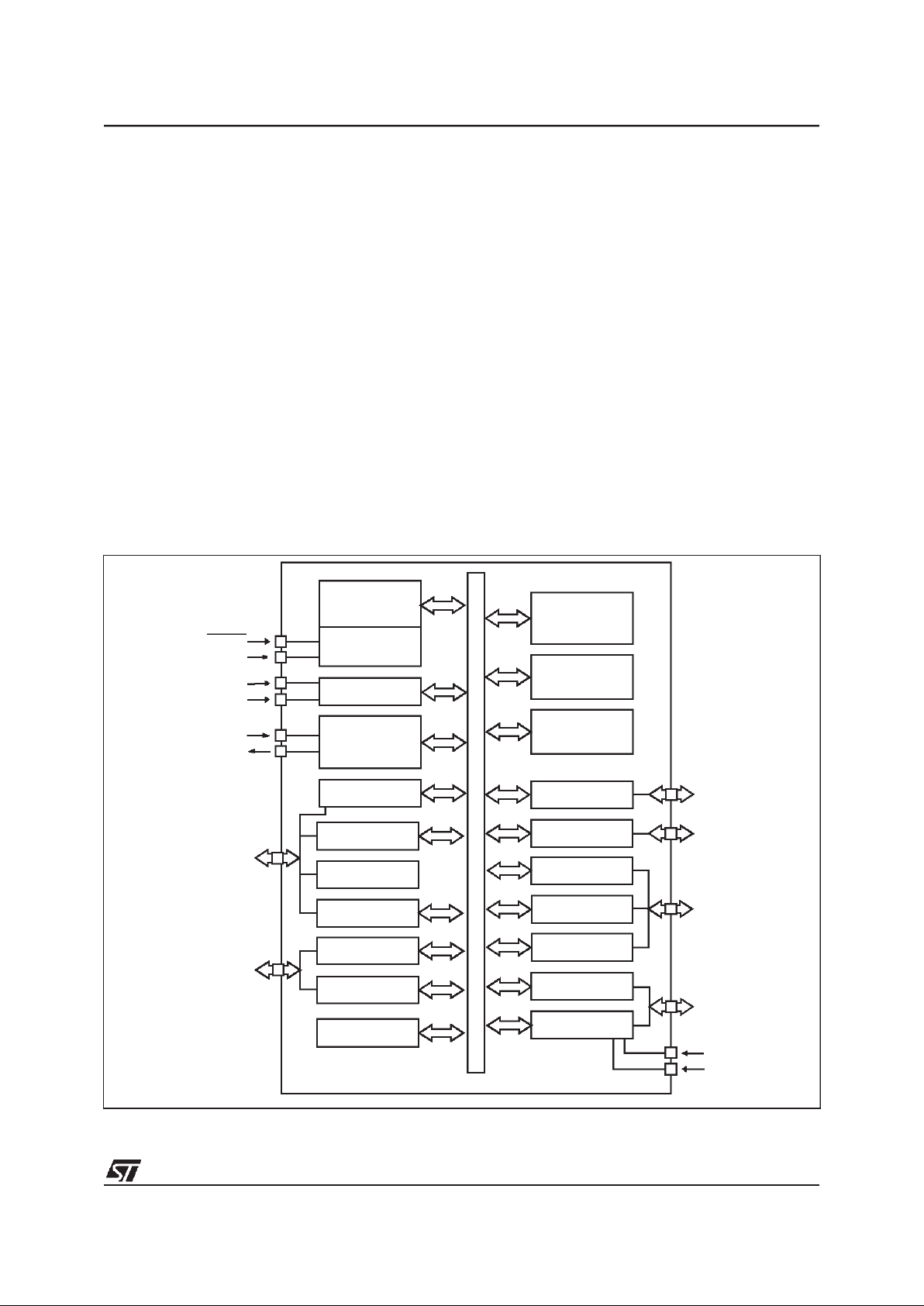
Figure 1. General Block Diagram
8-BIT CORE
ALU
ADDRESS AND DATA BUS
OSC1
ISPSEL
CONTROL
PROGRAM
(8K or 16K Bytes)
V
SS
RESET
PORT F
PF7,6,4,2:0
(6-BIT)
TIMER A
BEEP
PORT A
RAM
(384 or 512 Bytes)
PORT C
8-BIT ADC
V
DDA
V
SSA
PORT B
PB7:0
PORT E
PE7:0
SCI
TIMER B
PA7:0
PORT D
PD7:0
SPI
PC7:0
(8-BIT)
V
DD
EEPROM
(256 Bytes)
WATCHDOG
MULTI OSC
LVD
OSC2
MEMORY
MCC/RTC
+
CLOCK FILTER
(8-BIT for N versions)
(5-BIT for J versions)
(8-BIT for N versions)
(5-BIT for J versions)
(6-BIT for N versions)
(2-BIT for J versions)
(8-BIT for N versions)
(6-BIT for J versions)
ST72334J/N, ST72314J/N, ST72124J
6/148
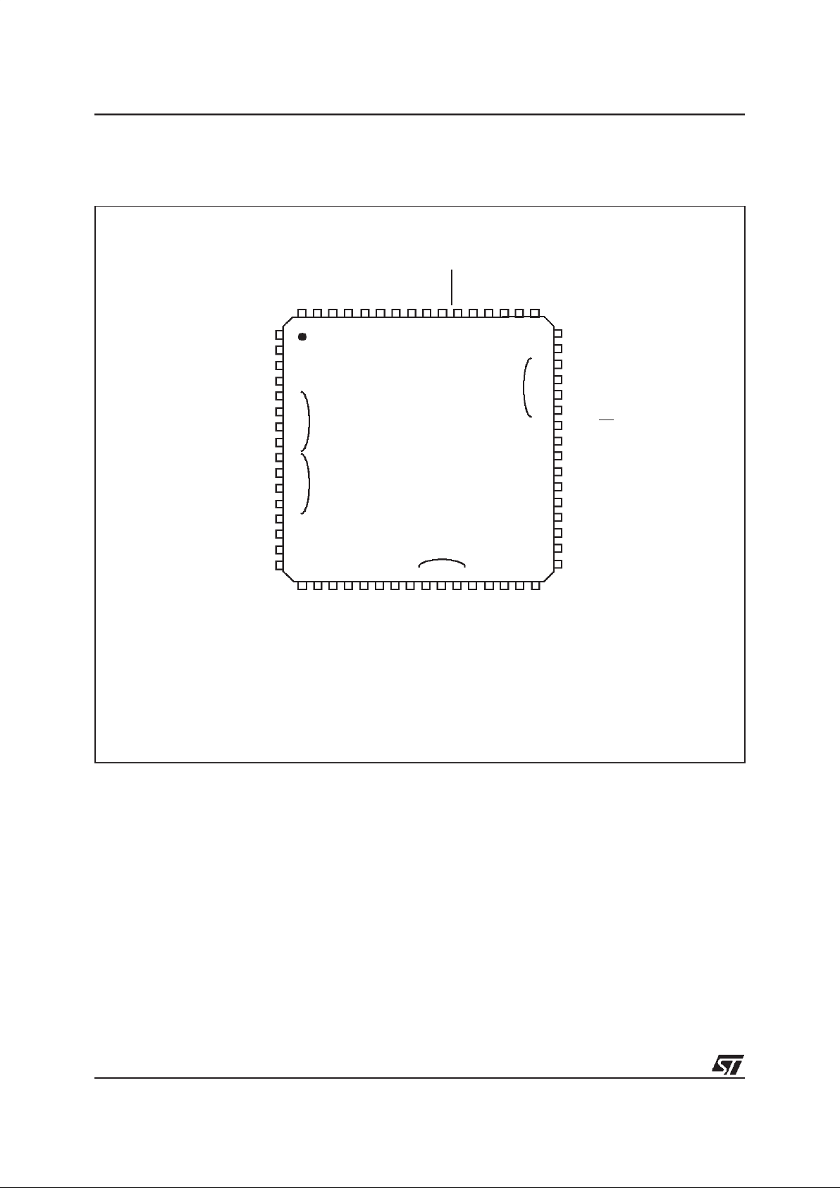
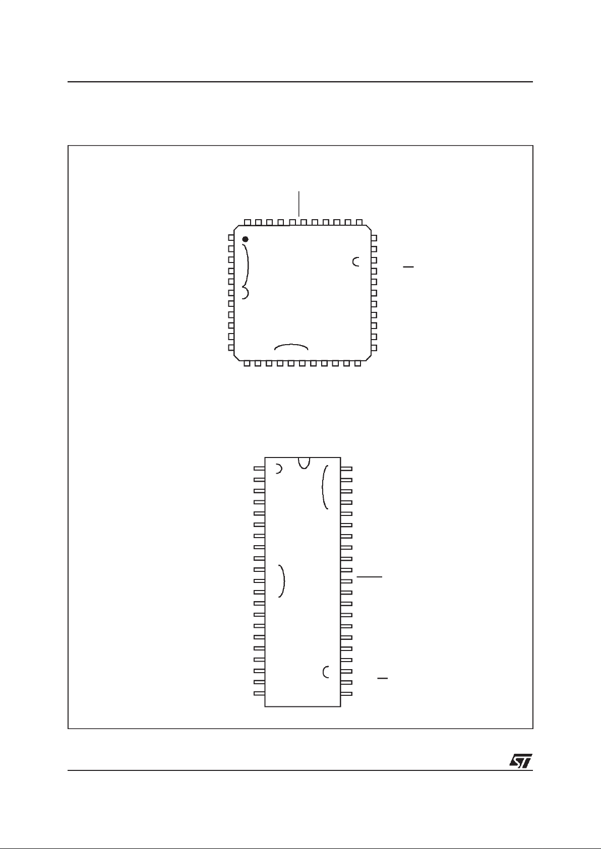
3 PIN DESCRIPTION
Figure 2. 64-Pin TQFP Package Pinout (N versions)
V
DDA
V
SSA
V
DD_3
V
SS_3
MCO / PF0
BEEP / PF1
PF2
NC
OCMP1_A / PF4
NC
ICAP1_A / (HS) PF6
EXTCLK_A / (HS) PF7
AIN4 / PD4
AIN5 / PD5
AIN6 / PD6
AIN7 / PD7
64 63 62 61 60 59 58 57 56 55 54 53 52 51 50 49
48
47
46
45
44
43
42
41
40
39
38
37
36
35
34
33
17 18 19 20 21 22 23 24 29 30 31 3225 26 27 28
1
2
3
4
5
6
7
8
9
10
11
12
13
14
15
16
ei2
ei3
ei0
ei1
PB0
PB1
PB2
PB3
PB4
PB5
PB6
PB7
AIN0 / PD0
AIN1 / PD1
AIN2 / PD2
AIN3 / PD3
(HS) PE4
(HS) PE5
(HS) PE6
(HS) PE7
PA1
PA0
PC7 / SS
PC6 / SCK / ISPCLK
PC5 / MOSI
PC4 / MISO / ISPDATA
PC3 (HS)/ ICAP1_B
PC2 (HS)/ ICAP2_B
PC1 / OCMP1_B
PC0 / OCMP2_B
V
SS_0
V
DD_0
V
SS_1
V
DD_1
PA3
PA2
V
DD
_2
OSC1
OSC2
V
SS
_2
NCNCRESET
ISPSEL
PA7 (HS)
PA6 (HS)
PA5 (HS)
PA4 (HS)
NCNCPE1 / RDI
PE0 / TDO
(HS) 20mA high sink capability
ei
x
associated external interrupt vector
ST72334J/N, ST72314J/N, ST72124J
7/148
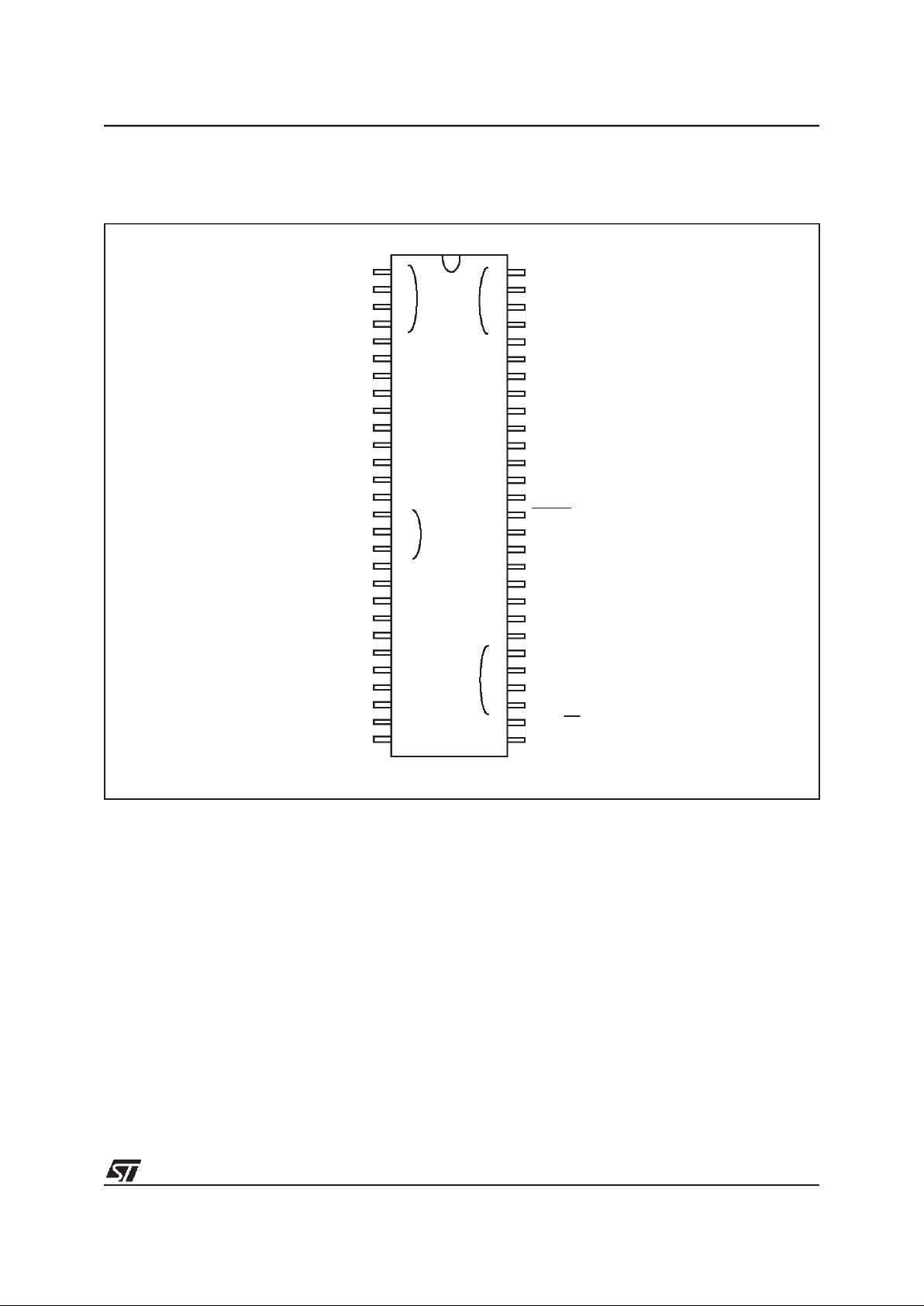
PIN DESCRIPTION (Cont’d)
Figure 3. 56-Pin SDIP Package Pinout (N versions)
52
51
50
49
48
47
46
45
44
43
42
41
16
15
1
2
3
4
5
6
7
8
9
10
11
12
13
14
53
54
55
56
PB4
PB5
BEEP / PF1
MCO / PF0
V
SSA
V
DDA
AIN7 / PD7
AIN6 / PD6
AIN5 / PD5
AIN2 / PD2
AIN1 / PD1
AIN0 / PD0
PB7
PB6
AIN4 / PD4
AIN3 / PD3
PB3
PB2
ISPSEL
RESET
V
SS
_2
OSC2
OSC1
V
DD
_2
PE0 / TDO
PE5 (HS)
PE6 (HS)
PE7 (HS)
PB0
PB1
PE4 (HS)
PE1 / RDI
ei3
ei0
ei2
ei1
21
20
17
18
19
V
DD_0
EXTCLK_A / (HS) PF7
ICAP1_A / (HS) PF6
OCMP1_A / PF4
PF2
40
39
38
37
36
V
SS_1
PA4 (HS)
PA5 (HS)
PA6 (HS)I
PA7 (HS)
23
22
OCMP2_B / PC0
V
SS_0
28
27
24
25
26
MOSI / PC5
ISPDATA/ MISO /PC4
ICAP1_B / (HS) PC3
ICAP2_B / (HS) PC2
OCMP1_B / PC1
35
34
PA3
V
DD_1
33
32
31
30
29
PC6 / SCK / ISPCLK
PC7 / SS
PA0
PA1
PA2
(HS) 20mA high sink capability
ei
x
associated external interrupt vector
ST72334J/N, ST72314J/N, ST72124J
8/148
PIN DESCRIPTION (Cont’d)
Figure 4. 44-Pin TQFP and 42-Pin SDIP Package Pinouts (J versions)
MCO / PF0
BEEP / PF1
PF2
OCMP1_A / PF4
ICAP1_A / (HS) PF6
EXTCLK_A / (HS) PF7
V
DD_0
V
SS_0
AIN5 / PD5
V
DDA
V
SSA
44 43 42 41 40 39 38 37 36 35 34
33
32
31
30
29
28
27
26
25
24
23
12 13 14 15 16 17 18 19 20 21 22
1
2
3
4
5
6
7
8
9
10
11
ei2
ei3
ei0
ei1
PB3
PB4
AIN0 / PD0
AIN1 / PD1
AIN2 / PD2
AIN3 / PD3
AIN4 / PD4
PE1 / RDI
PB0
PB1
PB2
PC6 / SCK / ISPCLK
PC5 / MOSI
PC4 / MISO / ISPDATA
PC3 (HS) / ICAP1_B
PC2 (HS) / ICAP2_B
PC1 / OCMP1_B
PC0 / OCMP2_B
V
SS_1
V
DD_1
PA3
PC7 / SS
V
SS
_2
RESET
ISPSEL
PA7 (HS)
PA6 (HS)
PA5 (HS)
PA4 (HS)
PE0 / TDO
V
DD
_2
OSC1
OSC2
38
37
36
35
34
33
32
31
30
29
28
27
16
15
1
2
3
4
5
6
7
8
9
10
11
12
13
14
39
40
41
42
PB4
AIN0 / PD0
OCMP2_B / PC0
EXTCLK_A / (HS) PF7
ICAP1_A / (HS) PF6
OCMP1_A / PF4
PF2
BEEP / PF1
MCO / PF0
AIN5 / PD5
AIN4 / PD4
AIN3 / PD3
AIN2 / PD2
AIN1 / PD1
V
SSA
V
DDA
PB3
PB2
PA4 (HS)
PA5 (HS)
PA6 (HS)
PA7 (HS)
ISPSEL
RESET
V
SS
_2
V
DD
_2
PE0 / TDO
PE1 / RDI
PB0
PB1
OSC1
OSC2
EI3
ei0
ei2
ei1
21
20
17
18
19
MOSI / PC5
ISPDATA / MISO / PC4
ICAP1_B / (HS) PC3
ICAP2_B/ (HS) PC2
OCMP1_B / PC1
26
25
24
23
22
PC6 / SCK / ISPCLK
PC7 / SS
PA3
V
DD_1
V
SS_1
(HS) 20mA high sink capability
ei
x
associated external interrupt vector
ST72334J/N, ST72314J/N, ST72124J
9/148
PIN DESCRIPTION (Cont’d)
For externalpin connection guidelines, refer to Section 15 ”ELECTRICAL CHARACTERISTICS” on page
105.
Legend / Abbreviations for Table 1:
Type: I = input, O = output, S = supply
Input level: A = Dedicated analog input
In/Output level: C = CMOS 0.3VDD/0.7VDD,
CT= CMOS 0.3VDD/0.7VDDwith input trigger
Output level: HS = 20mA high sink (on N-buffer only)
Port and control configuration:
– Input: float = floating, wpu = weak pull-up, int = interrupt1), ana = analog
– Output: OD = open drain2), PP = push-pull
Refer to Section 11 ”I/O PORTS” on page 37 for more details on the software configuration of the I/O
ports.
The RESETconfiguration ofeach pin is shown in bold. This configuration is valid as long as the device is
in reset state.
Table 1. Device Pin Description
Pin n°
Pin Name
Type
Level Port
Main
function
(after
reset)
Alternate function
TQFP64
SDIP56
QFP44
SDIP42
Input
Output
Input Output
float
wpu
int
ana
OD
PP
1 49 PE4 (HS) I/O CTHS X X X X Port E4
2 50 PE5 (HS) I/O C
T
HS X X X X Port E5
3 51 PE6 (HS) I/O C
T
HS X X X X Port E6
4 52 PE7 (HS) I/O C
T
HS X X X X Port E7
5 53 2 39 PB0 I/O C
T
X ei2 X X Port B0
6 54 3 40 PB1 I/O C
T
X ei2 X X Port B1
7 55 4 41 PB2 I/O C
T
X ei2 X X Port B2
8 56 5 42 PB3 I/O C
T
X ei2 X X Port B3
9 1 6 1 PB4 I/O C
T
X ei3 X X Port B4
10 2 PB5 I/O C
T
X ei3 X X Port B5
11 3 PB6 I/O C
T
X ei3 X X Port B6
12 4 PB7 I/O C
T
X ei3 X X Port B7
13 5 7 2 PD0/AIN0 I/O C
T
X X X X X Port D0 ADC Analog Input 0
14 6 8 3 PD1/AIN1 I/O C
T
X X X X X Port D1 ADC Analog Input 1
15 7 9 4 PD2/AIN2 I/O C
T
X X X X X Port D2 ADC Analog Input 2
16 8 10 5 PD3/AIN3 I/O C
T
X X X X X Port D3 ADC Analog Input 3
17 9 11 6 PD4/AIN4 I/O C
T
X X X X X Port D4 ADC Analog Input 4
18 10 12 7 PD5/AIN5 I/O C
T
X X X X X Port D5 ADC Analog Input 5
19 11 PD6/AIN6 I/O C
T
X X X X X Port D6 ADC Analog Input 6
20 12 PD7/AIN7 I/O C
T
X X X X X Port D7 ADC Analog Input 7
21 13 13 8 V
DDA
S Analog Power Supply Voltage
22 14 14 9 V
SSA
S Analog Ground Voltage
23 V
DD_3
S Digital Main Supply Voltage
ST72334J/N, ST72314J/N, ST72124J
10/148
24 V
SS_3
S Digital Ground Voltage
25 15 15 10 PF0/MCO I/O C
T
X ei1 X X Port F0 Main clock output (f
OSC
/2)
26 16 16 11 PF1/BEEP I/O C
T
X ei1 X X Port F1 Beep signal output
27 17 17 12 PF2 I/O C
T
X ei1 X X Port F2
28 NC Not Connected
29 18 18 13 PF4/OCMP1_A I/O C
T
X X X X Port F4 Timer A Output Compare 1
30 NC Not Connected
31 19 19 14 PF6 (HS)/ICAP1_A I/O C
T
HS X X X X Port F6 Timer A Input Capture 1
32 20 20 15 PF7 (HS)/EXTCLK_A I/O C
T
HS X X X X Port F7 Timer A External Clock Source
33 21 21 V
DD_0
S Digital Main Supply Voltage
34 22 22 V
SS_0
S Digital Ground Voltage
35 23 23 16 PC0/OCMP2_B I/O C
T
X X X X Port C0 Timer B Output Compare 2
36 24 24 17 PC1/OCMP1_B I/O C
T
X X X X Port C1 Timer B Output Compare 1
37 25 25 18 PC2 (HS)/ICAP2_B I/O C
T
HS X X X X Port C2 Timer B Input Capture 2
38 26 26 19 PC3 (HS)/ICAP1_B I/O C
T
HS X X X X Port C3 Timer B Input Capture 1
39 27 27 20 PC4/MISO I/O C
T
X X X X Port C4 SPI Master In / Slave Out Data
40 28 28 21 PC5/MOSI I/O C
T
X X X X Port C5 SPI Master Out / Slave In Data
41 29 29 22 PC6/SCK I/O C
T
X X X X Port C6 SPI Serial Clock
42 30 30 23 PC7/SS I/O C
T
X X X X Port C7 SPI Slave Select (active low)
43 31 PA0 I/O C
T
X ei0 X X Port A0
44 32 PA1 I/O C
T
X ei0 X X Port A1
45 33 PA2 I/O C
T
X ei0 X X Port A2
46 34 31 24 PA3 I/O C
T
X ei0 X X Port A3
47 35 32 25 V
DD_1
S Digital Main Supply Voltage
48 36 33 26 V
SS_1
S Digital Ground Voltage
49 37 34 27 PA4 (HS) I/O C
T
HS X X X X Port A4
50 38 35 28 PA5 (HS) I/O C
T
HS X X X X Port A5
51 39 36 29 PA6 (HS) I/O C
T
HS X T Port A6
52 40 37 30 PA7 (HS) I/O C
T
HS X T Port A7
53 41 38 31 ISPSEL I
Must be tied low in user mode. In programming mode when available, this pin
acts as In-Situ Programming mode selection.
54 42 39 32 RESET I/O C X X
Top priority non maskable interrupt (active low)
55 NC
Not Connected
56 NC
57 43 40 33 V
SS_3
S Digital Ground Voltage
58 44 41 34 OSC2
3)
O
Resonator oscillator inverter output or
capacitor input for RC oscillator
Pin n°
Pin Name
Type
Level Port
Main
function
(after
reset)
Alternate function
TQFP64
SDIP56
QFP44
SDIP42
Input
Output
Input Output
float
wpu
int
ana
OD
PP
ST72334J/N, ST72314J/N, ST72124J
11/148
Notes:
1. In the interrupt input column, “eix” defines the associated external interrupt vector. If the weak pull-up
column (wpu)is merged with theinterruptcolumn (int), then the I/O configuration is pull-up interruptinput,
else the configuration is floating interrupt input.
2. In the open drainoutput column, “T” defines a true open drain I/O(P-Buffer and protectiondiodeto V
DD
are not implemented). See Section 11”I/O PORTS” on page 37 and Section 15.8 ”I/O PORT PIN CHARACTERISTICS” on page 125 for more details.
3. OSC1 and OSC2 pins connect a crystal or ceramic resonator, an external RC, or an external source to
the on-chiposcillatorsee Section 3 ”PIN DESCRIPTION” onpage 6 and Section 15.5 ”CLOCK AND TIMING CHARACTERISTICS” on page 113 for more details.
59 45 42 35 OSC1
3)
I
External clock input orResonator oscillator inverter input or resistor input for RC
oscillator
60 46 43 36 V
DD_3
S Digital Main Supply Voltage
61 47 44 37 PE0/TDO I/O C
T
X X X X Port E0 SCI Transmit Data Out
62 48 1 38 PE1/RDI I/O C
T
X X X X Port E1 SCI Receive Data In
63 NC
Not Connected
64 NC
Pin n°
Pin Name
Type
Level Port
Main
function
(after
reset)
Alternate function
TQFP64
SDIP56
QFP44
SDIP42
Input
Output
Input Output
float
wpu
int
ana
OD
PP
ST72334J/N, ST72314J/N, ST72124J
12/148
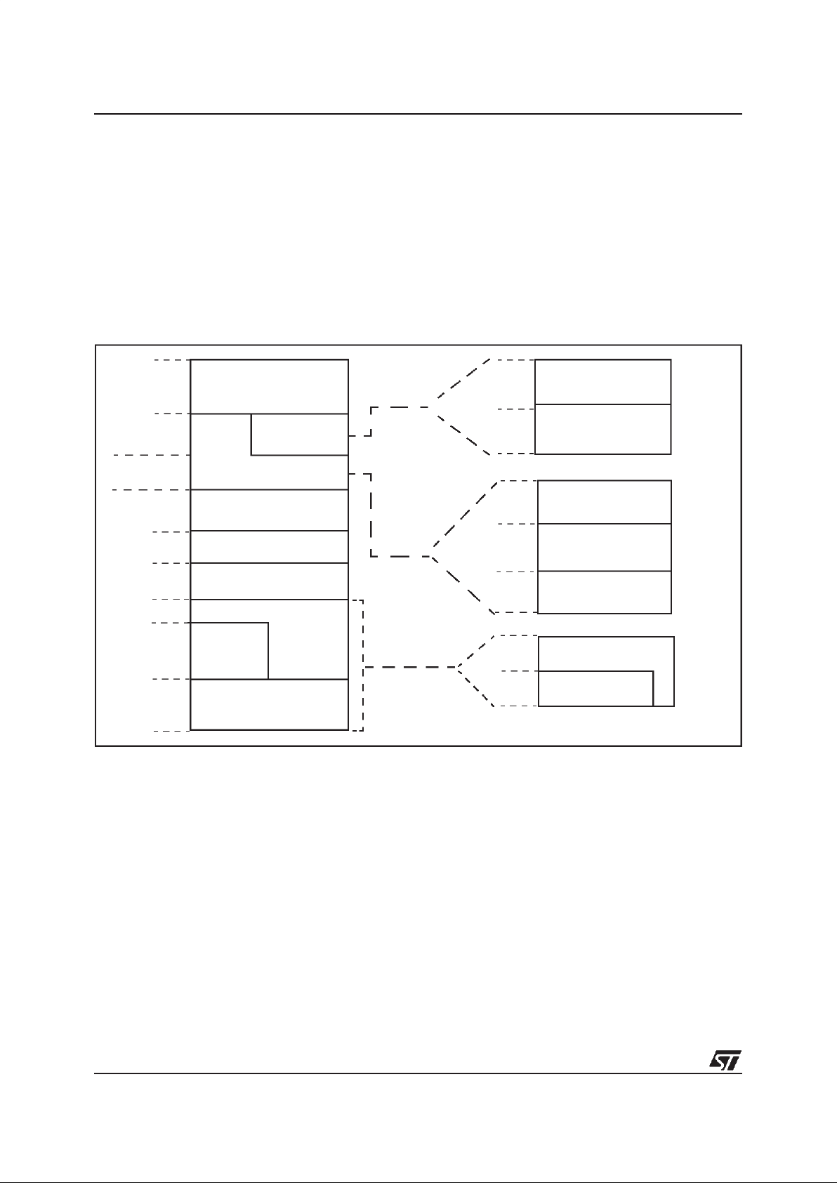
4 REGISTER & MEMORY MAP
As shown in the Figure 5, the MCU is capable of
addressing 64K bytes of memories and I/O registers.
The available memory locations consist of 128
bytes of register locations, 384 or 512 bytes of
RAM, up to 256 bytes of data EEPROM and 4 or
8 Kbytes of user program memory. The RAM
space includes up to 256 bytes for the stack from
0100h to 01FFh.
The highest address bytes contain the user reset
and interrupt vectors.
IMPORTANT: Memory locations marked as “Reserved” must never be accessed. Accessing a reseved area can have unpredicable effects on the
device.
Figure 5. Memory Map
0000h
Interrupt & Reset Vectors
HW Registers
027Fh
0080h
16-bit Addressing
RAM
007Fh
0200h / 0280h
0BFFh
Reserved
0080h
(see Table 2)
0C00h
FFDFh
FFE0h
FFFFh
(see Table 6 on page 32)
027Fh
C000h
Reserved
256 Bytes Data EEPROM
0CFFh
0D00h
BFFFh
00FFh
0100h
01FFh
0200h
8K Bytes
E000h
16K Bytes
Program
Short Addressing RAM
Zero page
0080h
00FFh
01FFh
01FFh
384 Bytes RAM
512 Bytes RAM
Stack or
16-bit Addressing RAM
0100h
Memory
Program
Memory
8 KBytes
E000h
C000h
16 KBytes
FFFFh
(128 Bytes)
(256 Bytes)
Short Addressing RAM
Zero page
Stack or
16-bit Addressing RAM
(128 Bytes)
(256 Bytes)

ST72334J/N, ST72314J/N, ST72124J
13/148
REGISTER & MEMORY MAP (Cont’d)
Table 2. Hardware Register Map
Address Block
Register
Label
Register Name
Reset
Status
Remarks
0000h
0001h
0002h
Port A
PADR
PADDR
PAOR
Port A Data Register
Port A Data Direction Register
Port A Option Register
00h
1)
00h
00h
R/W
R/W
R/W
2)
0003h Reserved Area (1 Byte)
0004h
0005h
0006h
Port C
PCDR
PCDDR
PCOR
Port C Data Register
Port C Data Direction Register
Port C Option Register
00h
1)
00h
00h
R/W
R/W
R/W
0007h Reserved Area (1 Byte)
0008h
0009h
000Ah
Port B
PBDR
PBDDR
PBOR
Port B Data Register
Port B Data Direction Register
Port B Option Register
00h
1)
00h
00h
R/W
R/W
R/W
2)
000Bh Reserved Area (1 Byte)
000Ch
000Dh
000Eh
Port E
PEDR
PEDDR
PEOR
Port E Data Register
Port E Data Direction Register
Port E Option Register
00h
1)
00h
00h
R/W
R/W
R/W
2)
000Fh Reserved Area (1 Byte)
0010h
0011h
0012h
Port D
PDDR
PDDDR
PDOR
Port D Data Register
Port D Data Direction Register
Port D Option Register
00h
1)
00h
00h
R/W
R/W
R/W
2)
0013h Reserved Area (1 Byte)
0014h
0015h
0016h
Port F
PFDR
PFDDR
PFOR
Port F Data Register
Port F Data Direction Register
Port F Option Register
00h
1)
00h
00h
R/W
R/W
R/W
0017h
to
001Fh
Reserved Area (9 Bytes)
0020h MISCR1 Miscellaneous Register 1 00h R/W
0021h
0022h
0023h
SPI
SPIDR
SPICR
SPISR
SPI Data I/O Register
SPI Control Register
SPI Status Register
xxh
0xh
00h
R/W
R/W
Read Only
0024h
to
0028h
Reserved Area (5 Bytes)
0029h MCC MCCSR Main Clock Control / Status Register 01h R/W

ST72334J/N, ST72314J/N, ST72124J
14/148
002Ah WATCHDOG WDGCR Watchdog Control Register 7Fh R/W
002Bh CRSR Clock, Reset, Supply Control / Status Register 000x 000x R/W
002Ch Data-EEPROM EECSR Data-EEPROM Control/Status Register 00h R/W
002Dh
0030h
Reserved Area (4 Bytes)
0031h
0032h
0033h
0034h
0035h
0036h
0037h
0038h
0039h
003Ah
003Bh
003Ch
003Dh
003Eh
003Fh
TIMER A
TACR2
TACR1
TASR
TAIC1HR
TAIC1LR
TAOC1HR
TAOC1LR
TACHR
TACLR
TAACHR
TAACLR
TAIC2HR
TAIC2LR
TAOC2HR
TAOC2LR
Timer A Control Register 2
Timer A Control Register 1
Timer A Status Register
Timer A Input Capture 1 High Register
Timer A Input Capture 1 Low Register
Timer A Output Compare 1 High Register
Timer A Output Compare 1 Low Register
Timer A Counter High Register
Timer A Counter Low Register
Timer A Alternate Counter High Register
Timer A Alternate Counter Low Register
Timer A Input Capture 2 High Register
Timer A Input Capture 2 Low Register
Timer A Output Compare 2 High Register
Timer A Output Compare 2 Low Register
00h
00h
xxh
xxh
xxh
80h
00h
FFh
FCh
FFh
FCh
xxh
xxh
80h
00h
R/W
R/W
Read Only
Read Only
Read Only
R/W
R/W
Read Only
Read Only
Read Only
Read Only
Read Only
3)
Read Only
3)
R/W
3)
R/W
3)
0040h MISCR2 Miscellaneous Register 2 00h R/W
0041h
0042h
0043h
0044h
0045h
0046h
0047h
0048h
0049h
004Ah
004Bh
004Ch
004Dh
004Eh
004Fh
TIMER B
TBCR2
TBCR1
TBSR
TBIC1HR
TBIC1LR
TBOC1HR
TBOC1LR
TBCHR
TBCLR
TBACHR
TBACLR
TBIC2HR
TBIC2LR
TBOC2HR
TBOC2LR
Timer B Control Register 2
Timer B Control Register 1
Timer B Status Register
Timer B Input Capture 1 High Register
Timer B Input Capture 1 Low Register
Timer B Output Compare 1 High Register
Timer B Output Compare 1 Low Register
Timer B Counter High Register
Timer B Counter Low Register
Timer B Alternate Counter High Register
Timer B Alternate Counter Low Register
Timer B Input Capture 2 High Register
Timer B Input Capture 2 Low Register
Timer B Output Compare 2 High Register
Timer B Output Compare 2 Low Register
00h
00h
xxh
xxh
xxh
80h
00h
FFh
FCh
FFh
FCh
xxh
xxh
80h
00h
R/W
R/W
Read Only
Read Only
Read Only
R/W
R/W
Read Only
Read Only
Read Only
Read Only
Read Only
Read Only
R/W
R/W
0050h
0051h
0052h
0053h
0054h
0055h
0056h
0057h
SCI
SCISR
SCIDR
SCIBRR
SCICR1
SCICR2
SCIERPR
SCIETPR
SCI Status Register
SCI Data Register
SCI Baud Rate Register
SCI Control Register 1
SCI Control Register 2
SCI Extended Receive Prescaler Register
Reserved area
SCI Extended Transmit Prescaler Register
C0h
xxh
00xx xxxx
xxh
00h
00h
---
00h
Read Only
R/W
R/W
R/W
R/W
R/W
R/W
Address Block
Register
Label
Register Name
Reset
Status
Remarks

ST72334J/N, ST72314J/N, ST72124J
15/148
Legend: x=undefined, R/W=read/write
Notes:
1. The contentsof the I/O port DR registers are readable only in output configuration. In input configuration, the values of the I/O pins are returnedinstead of the DR register contents.
2. The bits corresponding to unavailable pins are forced to 1 byhardware, affecting accordingly the reset
status value. These bits must always keep their reset value.
3. External pin not available.
0058h
006Fh
Reserved Area (24 Bytes)
0070h
0071h
ADC
ADCDR
ADCCSR
Data Register
Control/Status Register
xxh
00h
Read Only
R/W
0072h
to
007Fh
Reserved Area (14 Bytes)
Address Block
Register
Label
Register Name
Reset
Status
Remarks
ST72334J/N, ST72314J/N, ST72124J
16/148
5 FLASH PROGRAM MEMORY
5.1 INTRODUCTION
FLASH devices have a single voltage non-volatile
FLASH memory that may be programmed in-situ
(or plugged in a programming tool) on a byte-bybyte basis.
5.2 MAIN FEATURES
■ Remote In-Situ Programming (ISP) mode
■ Up to 16 bytes programmedin the same cycle
■ MTP memory (Multiple Time Programmable)
■ Read-out memory protection against piracy
5.3 STRUCTURAL ORGANISATION
The FLASH program memory is organised in a
single 8-bit wide memory block which can be used
for storing both code and data constants.
The FLASH program memory is mappedin the upper part ofthe ST7 addressing space and includes
the reset and interrupt user vector area .
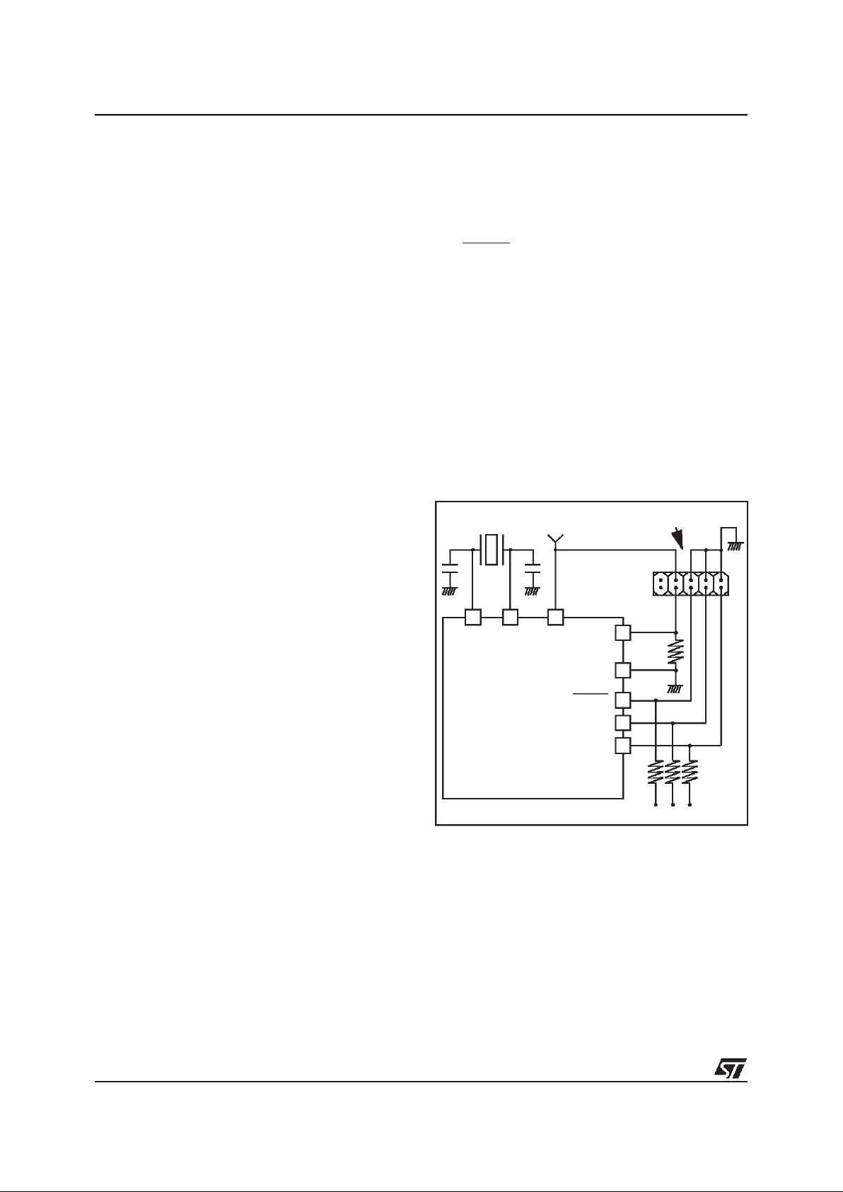
5.4 IN-SITU PROGRAMMING (ISP) MODE
The FLASH program memory canbe programmed
using Remote ISP mode. This ISP mode allows
the contentsoftheST7program memory to be updated usingastandard ST7 programming tools after the device is mounted on the application board.
This feature can be implemented with a minimum
number of added components and board area impact.
An exampleRemote ISP hardware interface to the
standard ST7 programming tool is described below. For more details on ISP programming, refer to
the ST7 Programming Specification.
Remote ISP Overview
The Remote ISP mode is initiatedby a specific sequence on the dedicated ISPSEL pin.
The Remote ISP is performedin three steps:
– Selection of the RAM execution mode
– Download of Remote ISP codein RAM
– Execution ofRemote ISP code in RAM to pro-
gram the user program into the FLASH
Remote ISP hardware configuration
In Remote ISP mode, the ST7 has to be supplied
with power (VDDand VSS) and a clock signal (oscillator and application crystal circuit for example).
This mode needs five signals (plus the VDDsignal
if necessary) to be connected to the programming
tool. This signals are:
– RESET: device reset
–VSS: device ground power supply
– ISPCLK: ISP outputserial clock pin
– ISPDATA: ISP input serial data pin
– ISPSEL: Remote ISP modeselection. Thispin
must be connected to VSSon the application
board through a pull-down resistor.
If any of thesepins areused for other purposeson
the application, a serial resistor has to be implemented to avoid a conflict ifthe other deviceforces
the signal level.
Figure 6 shows a typical hardware interface to a
standard ST7 programming tool. For more details
on the pin locations, refer to the device pinout description.
Figure 6. Typical Remote ISP Interface
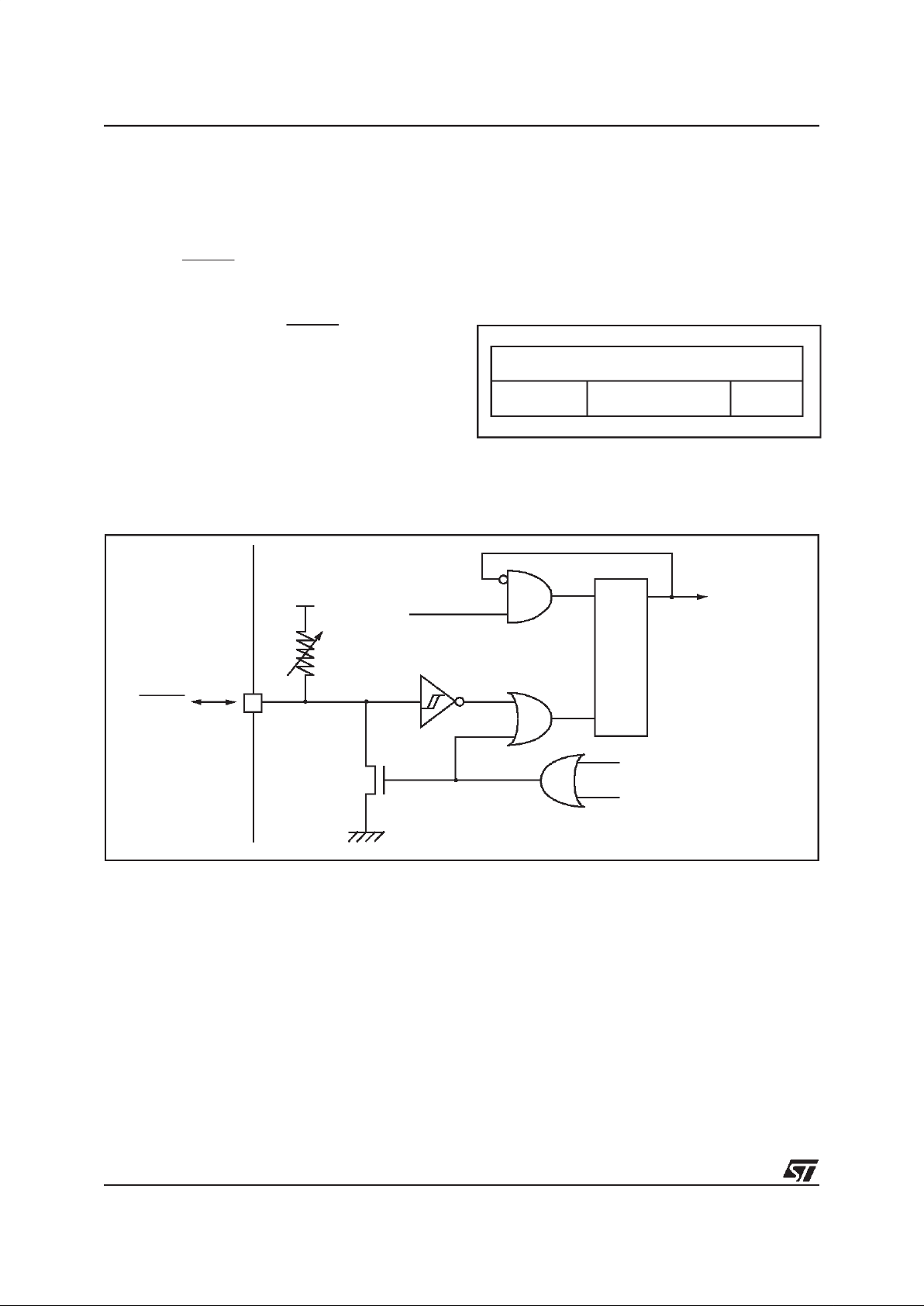
5.5 MEMORY READ-OUT PROTECTION
The read-out protection is enabled through an option bit.
For FLASH devices, when this option is selected,
the program and data stored in the FLASH memory are protected against read-out piracy (including
a re-write protection). When this protection option
is removed the entire FLASH program memory is
first automatically erased. However, the E2PROM
data memory (when available) can be protected
only with ROM devices.
ISPSEL
V
SS
RESET
ISPCLK
ISPDATA
OSC1
OSC2
V
DD
ST7
HE10 CONNECTOR TYPE
TO PROGRAMMINGTOOL
10KΩ
C
L0
C
L1
APPLICATION
47KΩ
1
XTAL
ST72334J/N, ST72314J/N, ST72124J
17/148
6 DATA EEPROM
6.1 INTRODUCTION
The Electrically Erasable Programmable Read
Only Memory can be used as a non volatile backup for storing data.Using the EEPROM requires a
basic access protocol described in this chapter.
6.2 MAIN FEATURES
■ Up to 16 Bytes programmed in the same cycle
■ EEPROM mono-voltage (charge pump)
■ Chained erase and programming cycles
■ Internal control of the global programming cycle
duration
■ End of programming cycle interrupt flag
■ WAIT mode management
Figure 7. EEPROM Block Diagram
EECSR
EEPROM INTERRUPT
FALLING
EDGE
HIGH VOLTAGE
PUMP
IE LAT00000 PGM
EEPROMRESERVED
DETECTOR
EEPROM
MEMORY MATRIX
(1 ROW = 16 x 8 BITS)
ADDRESS
DECODER
DATA
MULTIPLEXER
16 x 8 BITS
DATA LATCHES
ROW
DECODER
DATA BUS
4
4
4
128128
ADDRESS BUS
ST72334J/N, ST72314J/N, ST72124J
18/148
DATA EEPROM (Cont’d)
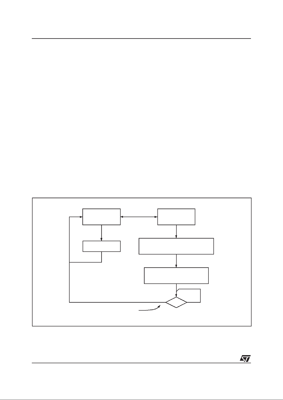
6.3 MEMORY ACCESS
The Data EEPROM memory read/write access
modes are controlled by the LAT bit of the EEPROM Control/Status register (EECSR). The flowchart inFigure 8 describes these different memory
access modes.
Read Operation (LAT=0)
The EEPROM canbe read as a normal ROM location when the LAT bit of the EECSR register is
cleared. Ina read cycle, the byte to be accessed is
put onthedatabusin less than 1CPUclock cycle.
This means that reading data from EEPROM
takes the same time as reading data from
EPROM, but this memory cannot be used to execute machine code.
Write Operation (LAT=1)
To access the write mode, the LAT bit has to be
set by software (the PGM bit remains cleared).
When a write access to the EEPROM area occurs,
the value is latched inside the 16 data latches according to its address.
When PGM bit is set by the software, all the previous bytes written in the data latches(up to16) are
programmed in the EEPROM cells. The effective
high address (row) is determined by the last EEPROM write sequence. To avoid wrong programming, the user must take care that all the bytes
written between two programming sequences
have the same high address: only the four Least
Significant Bits of the address can change.
At the end of the programming cycle, the PGM and
LAT bits are cleared simultaneously, and an interrupt is generated if the IE bitis set. The Data EEPROM interrupt request is cleared by hardware
when the Data EEPROM interrupt vector is
fetched.
Note: Care should be taken during the programming cycle. Writing to the same memory location
will over-program the memory (logical AND between the two write access data result) because
the data latches are only cleared at the end of the
programming cycle and by thefalling edge of LAT
bit.
It is not possible toread the latched data.
This note is ilustrated by the Figure 9.
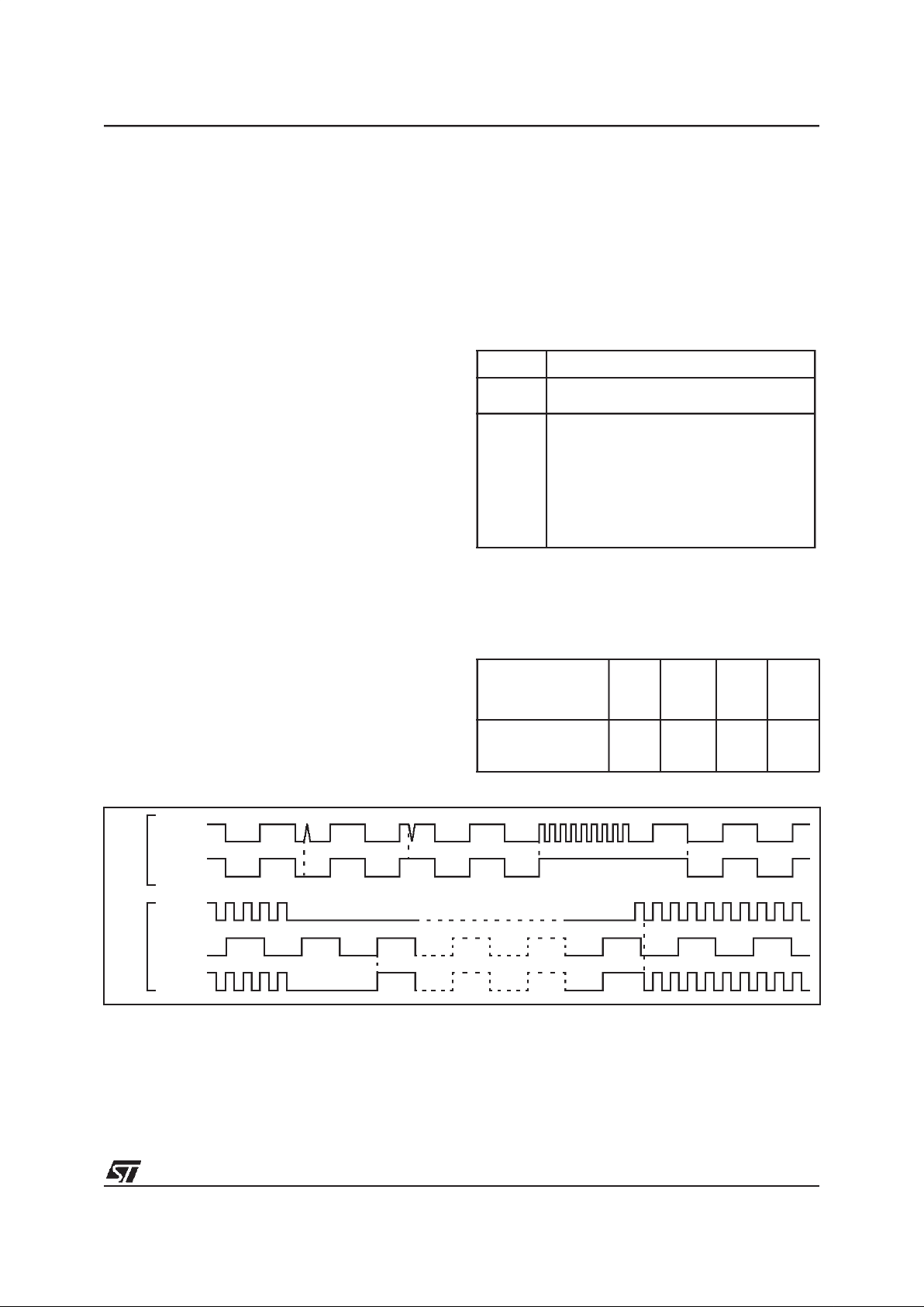
Figure 8. Data EEPROM ProgrammingFlowchart
READ MODE
LAT=0
PGM=0
WRITEMODE
LAT=1
PGM=0
READ BYTES
IN EEPROM AREA
WRITE UP TO 16 BYTES
IN EEPROM AREA
(with the same 12 MSB of the address)
START PROGRAMMING CYCLE
LAT=1
PGM=1 (set by software)
LAT
INTERRUPT GENERATION
IF IE=1 0 1
CLEARED BY HARDWARE
ST72334J/N, ST72314J/N, ST72124J
19/148
DATA EEPROM (Cont’d)
6.4 POWER SAVING MODES
Wait mode
The DATAEEPROMcan enter WAIT mode on execution of the WFI instruction of the microcontroller. The DATA EEPROM will immediately enter
this mode if there is no programming in progress,
otherwise the DATA EEPROM will finish the cycle
and then enter WAIT mode.
Halt mode
The DATA EEPROM immediatly enters HALT
mode if themicrocontroller executes the HALT instruction. Therefore the EEPROM will stop the
function in progress, and data may be corrupted.
6.5 ACCESS ERROR HANDLING
If a read access occurs while LAT=1, then the data
bus will not be driven.
If a write access occurs while LAT=0, then the
data on the bus will not be latched.
If a programming cycle is interrupted (by software/
RESET action), the memory data will not be guaranteed.
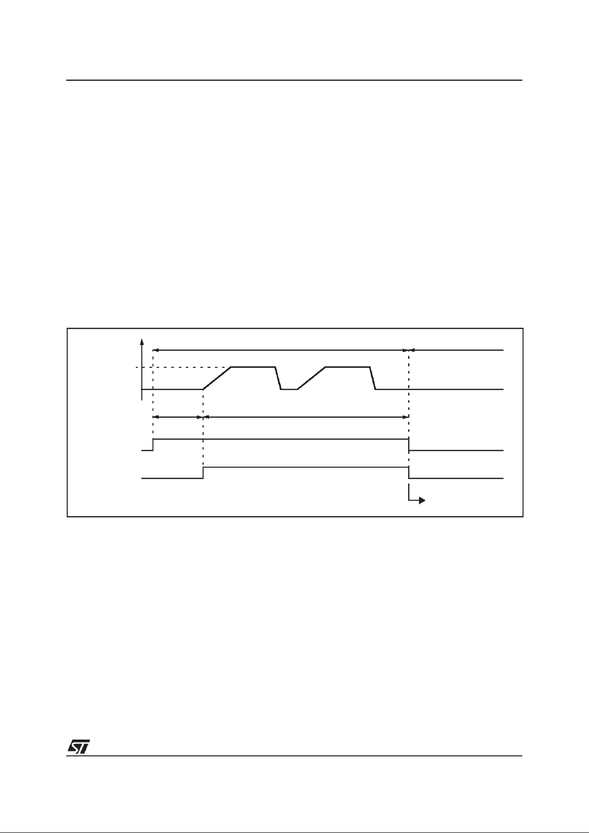
Figure 9. Data EEPROM ProgrammingCycle
LAT
ERASE CYCLE WRITE CYCLE
PGM
t
PROG
READ OPERATION NOT POSSIBLE
WRITE OF
DATA LATCHES
READ OPERATION POSSIBLE
INTERNAL
PROGRAMMING
VOLTAGE
EEPROM INTERRUPT

ST72334J/N, ST72314J/N, ST72124J
20/148
DATA EEPROM (Cont’d)
6.6 REGISTER DESCRIPTION
CONTROL/STATUS REGISTER (CSR)
Read/Write
Reset Value: 0000 0000 (00h)
Bit 7:3 = Reserved, forced by hardware to 0.
Bit 2 = IE
Interrupt enable
Thisbitissetandclearedbysoftware.Itenables the
Data EEPROM interrupt capability when the PGM
bit iscleared by hardware. The interrupt request is
automatically cleared when thesoftware enters the
interrupt routine.
0: Interrupt disabled
1: Interrupt enabled
Bit 1 = LAT
Latch Access Transfer
This bit is set by software. It is cleared by hardware at the end of the programming cycle. It can
only be cleared by software if PGM bit is cleared.
0: Read mode
1: Write mode
Bit 0 = PGM
Programming controland status
Thisbitis setbysoftware tobegin theprogramming
cycle. At the end of the programming cycle, this bit
isclearedby hardwareandaninterruptisgenerated
if theITE bit is set.
0: Programming finished or not yet started
1: Programming cycle isin progress
Note: if thePGM bit is cleared during the programming cycle, the memory data is not guaranteed
Table 3. DATA EEPROM Register Map and Reset Values
6.7 READ-OUT PROTECTION OPTION
The Data EEPROM can be optionally read-out
protected in ST72334 ROM devices (see option
list onpage 145). ST72C334 Flash devices do not
have this protection option.
70
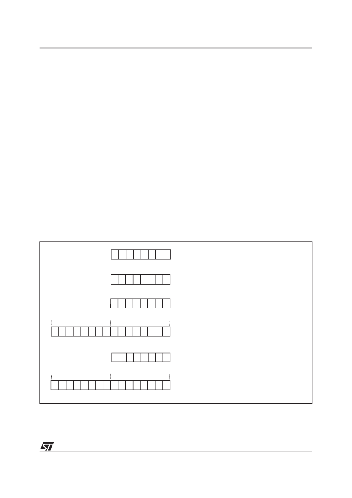
00000IELATPGM
Address
(Hex.)
Register
Label
76543210
002Ch
EECSR
Reset Value
00000IE0
RWM
0
PGM
0
ST72334J/N, ST72314J/N, ST72124J
21/148
7 CENTRAL PROCESSING UNIT
7.1 INTRODUCTION
This CPU has a full 8-bit architecture and contains
six internal registers allowing efficient 8-bit data
manipulation.
7.2 MAIN FEATURES
■ 63 basic instructions
■ Fast 8-bit by 8-bit multiply
■ 17 main addressing modes
■ Two 8-bit index registers
■ 16-bit stack pointer
■ Low power modes
■ Maskable hardware interrupts
■ Non-maskable software interrupt
7.3 CPU REGISTERS
The 6 CPU registers shown in Figure 10 are not
present in the memory mapping and are accessed
by specific instructions.
Accumulator (A)
The Accumulator is an 8-bit general purpose register used to hold operands and the results of the
arithmetic and logic calculations and to manipulate
data.
Index Registers (X and Y)
In indexed addressing modes, these 8-bitregisters
are used to create either effective addresses or
temporary storage areas for data manipulation.
(The Cross-Assembler generates a precede instruction (PRE) to indicate that the following instruction refers to the Y register.)
The Y registeris not affectedby the interrupt automatic procedures (notpushed to and popped from
the stack).
Program Counter (PC)
The program counter is a 16-bit register containing
the address of the next instruction to be executed
by the CPU. It is made of two 8-bit registers PCL
(Program Counter Low which is the LSB) andPCH
(Program CounterHigh which is the MSB).
Figure 10. CPU Registers
ACCUMULATOR
X INDEX REGISTER
Y INDEX REGISTER
STACK POINTER
CONDITION CODE REGISTER
PROGRAM COUNTER
70
1C11HI NZ
RESET VALUE = RESET VECTOR @ FFFEh-FFFFh
70
70
70
0
7
15 8
PCH
PCL
15
87 0
RESET VALUE = STACKHIGHER ADDRESS
RESET VALUE =
1X11X1XX
RESET VALUE = XXh
RESET VALUE = XXh
RESET VALUE= XXh
X = Undefined Value

ST72334J/N, ST72314J/N, ST72124J
22/148
CPU REGISTERS (Cont’d)
CONDITION CODE REGISTER (CC)
Read/Write
Reset Value: 111x1xxx
The 8-bit Condition Code register contains the interrupt mask and four flags representative of the
result ofthe instruction just executed. This register
can also be handled by the PUSH and POP instructions.
These bits can be individually tested and/or controlled by specific instructions.
Bit 4 = H
Half carry
.
This bit is set by hardware whena carryoccursbetween bits 3 and 4 of the ALU during an ADD or
ADC instruction. It is reset by hardware during the
same instructions.
0: No half carry has occurred.
1: A half carry has occurred.
This bit is tested using the JRH or JRNH instruction. The H bit is useful in BCD arithmetic subroutines.
Bit 3 = I
Interrupt mask
.
This bit is set by hardware when entering in interrupt or by software to disable all interrupts except
the TRAP software interrupt. This bit is cleared by
software.
0: Interrupts are enabled.
1: Interrupts are disabled.
This bit is controlledby the RIM, SIM and IRET instructions and is tested by the JRM and JRNM instructions.
Note: Interrupts requested while I is set are
latched and can be processed when I is cleared.
By default an interrupt routine is not interruptable
because the I bit is set by hardware when you enter it and resetby the IRETinstruction at the endof
the interrupt routine. If the I bit is cleared by software in the interrupt routine, pending interrupts are
serviced regardless of the priority level of the current interrupt routine.
Bit 2 = N
Negative
.
This bit is set and cleared by hardware. It is representative of the result sign of the last arithmetic,
logical or data manipulation. It is a copy of the 7
th
bit of the result.
0:Theresultof the last operation is positive or null.
1: The result of the last operation is negative
(i.e. the most significant bit is a logic 1).
This bit isaccessed bythe JRMI andJRPL instructions.
Bit 1 = Z
Zero
.
This bit is set and cleared by hardware. Thisbit indicates that the result of the last arithmetic, logical
or data manipulation is zero.
0: The result of the last operation is different from
zero.
1: The result of the last operation is zero.
This bit is accessed by the JREQ and JRNE test
instructions.
Bit 0 = C
Carry/borrow.
This bit is set and cleared by hardware and software. It indicates an overflow or an underflow has
occurred during the last arithmetic operation.
0: No overflow or underflow has occurred.
1: An overflow or underflow hasoccurred.
This bit is driven by the SCF and RCF instructions
and tested by the JRC and JRNC instructions. It is
also affected by the “bit test and branch”, shift and
rotate instructions.
70
111HINZC
ST72334J/N, ST72314J/N, ST72124J
23/148
CENTRAL PROCESSING UNIT (Cont’d)
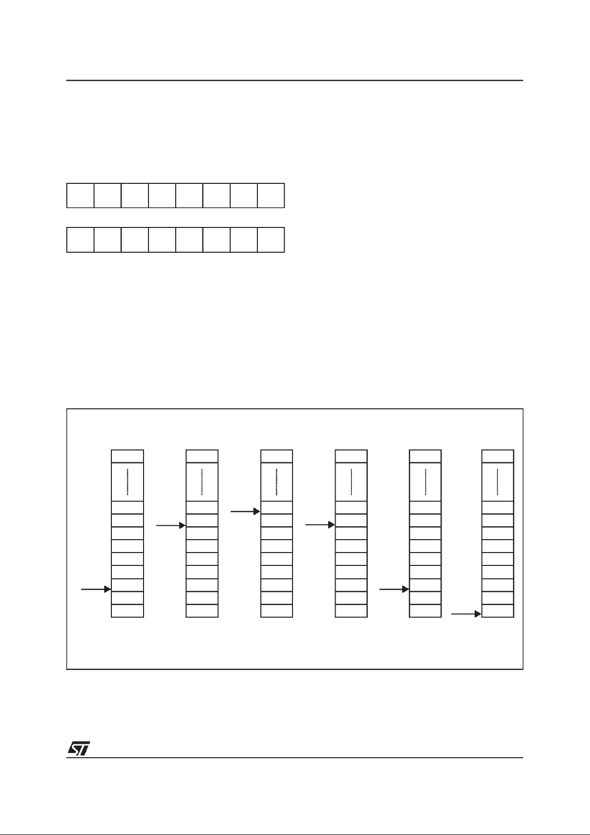
Stack Pointer (SP)
Read/Write
Reset Value: 01 FFh
The Stack Pointer is a 16-bit register which is always pointingto the next free location in the stack.
It isthen decremented after data has been pushed
onto the stack and incremented before data is
popped from the stack (see Figure 11).
Since the stack is 256 bytes deep, the 8th most
significant bits are forced by hardware. Following
an MCU Reset, or after a Reset Stack Pointer instruction (RSP), the Stack Pointer contains its reset value (the SP7 to SP0 bits areset) which is the
stack higher address.
The least significant byte of the Stack Pointer
(called S) can be directly accessed by a LD instruction.
Note: When the lower limit is exceeded, the Stack
Pointer wraps around to the stack upper limit, without indicating the stack overflow. The previously
stored information is then overwritten and therefore lost. The stack also wrapsin case of anunderflow.
The stack is used to save the return address during a subroutine call and the CPU context during
an interrupt. The user may also directly manipulate
the stack by meansof the PUSH and POP instructions. In the case of an interrupt, the PCL is stored
at the first location pointed to by the SP. Then the
other registers are stored in the next locations as
shown in Figure 11.
– When an interrupt is received, the SP is decre-
mented and the context is pushed on the stack.
– On return from interrupt, the SP is incremented
and the context is popped from thestack.
A subroutine call occupies twolocations and an interrupt five locations in the stack area.
Figure 11. Stack Manipulation Example
15 8
00000001
70
SP7 SP6 SP5 SP4 SP3 SP2 SP1 SP0
PCH
PCL
SP
PCH
PCL
SP
PCL
PCH
X
A
CC
PCH
PCL
SP
PCL
PCH
X
A
CC
PCH
PCL
SP
PCL
PCH
X
A
CC
PCH
PCL
SP
SP
Y
CALL
Subroutine
Interrupt
Event
PUSH Y POP Y IRET
RET
or RSP
@ 01FFh
@ 0100h
Stack Higher Address = 01FFh
Stack Lower Address =
0100h
ST72334J/N, ST72314J/N, ST72124J
24/148
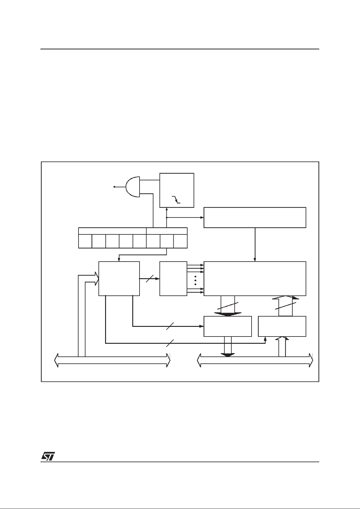
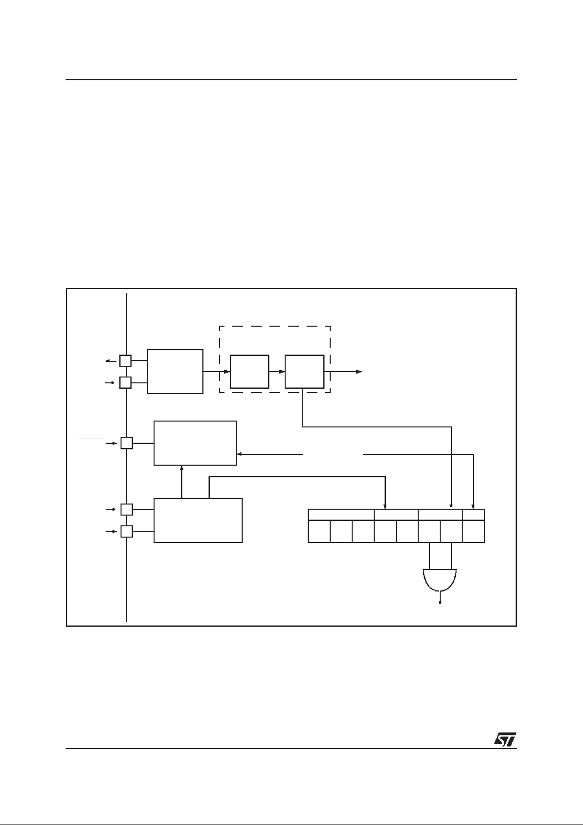
8 SUPPLY, RESET AND CLOCK MANAGEMENT
The ST72334J/N, ST72314J/N and ST72124J microcontrollers include a range of utility features for
securing the application in critical situations (for
example in case of a power brown-out), and reducing the number of external components. An
overview is shown in Figure 12.
See Section 15 ”ELECTRICAL CHARACTERISTICS” on page 105 for more details.
Main Features
■ Supply Manager with main supply low voltage
detection (LVD)
■ Reset Sequence Manager (RSM)
■ Multi-Oscillator (MO)
– 4 Crystal/Ceramic resonator oscillators
– 1 External RC oscillator
– 1 Internal RC oscillator
■ Clock Security System (CSS)
– Clock Filter
– Backup Safe Oscillator
Figure 12. Clock, Reset and Supply Block Diagram
IE D00 0 0 RF RF
CRSR
CSS WDG
f
OSC
CSS INTERRUPT
LVD
LOW VOLTAGE
DETECTOR
(LVD)
MULTI-
OSCILLATOR
(MO)
FROM
WATCHDOG
PERIPHERAL
OSC1
RESET
VDD
VSS
RESET SEQUENCE
MANAGER
(RSM)
CLOCK
FILTER
SAFE
OSC
CLOCK SECURITYSYSTEM
(CSS)
OSC2
TO
MAIN CLOCK
CONTROLLER
ST72334J/N, ST72314J/N, ST72124J
25/148
8.1 LOW VOLTAGE DETECTOR (LVD)
To allow the integration of power management
features in the application, the Low Voltage Detector function (LVD) generates a static reset when
the VDDsupply voltage is below a V
IT-
reference
value. This means that it secures the power-up as
well as the power-down keeping the ST7 in reset.
The V
IT-
referencevalue fora voltage drop is lower
than the V
IT+
referencevalue forpower-on in order
to avoid a parasitic reset when theMCUstarts running and sinks current on the supply (hysteresis).
The LVD Reset circuitry generates a reset when
VDDis below:
–V
IT+
when VDDis rising
–V
IT-
when VDDis falling
The LVD function is illustrated in the Figure 13.
Provided the minimum VDDvalue (guaranteed for
the oscillator frequency) is above V
IT-
, the MCU
can only be in two modes:
– under full software control
– in static safe reset
In these conditions, secure operation is always ensured for the application without the need for external reset hardware.
During aLow Voltage Detector Reset, the RESET
pin is held low, thus permitting the MCU to reset
other devices.
Notes:
1. The LVD allows the device to be used without
any external RESET circuitry.
2. Three different reference levels are selectable
through the option byte according to the application requirement.
LVD application note
Application software can detect a reset caused by
the LVD by reading the LVDRF bit in the CRSR
register.
This bit is set by hardware when a LVD reset is
generated and cleared by software (writing zero).
Figure 13. Low Voltage Detector vs Reset
V
DD
V
IT+
RESET
V
IT-
V
hyst
ST72334J/N, ST72314J/N, ST72124J
26/148
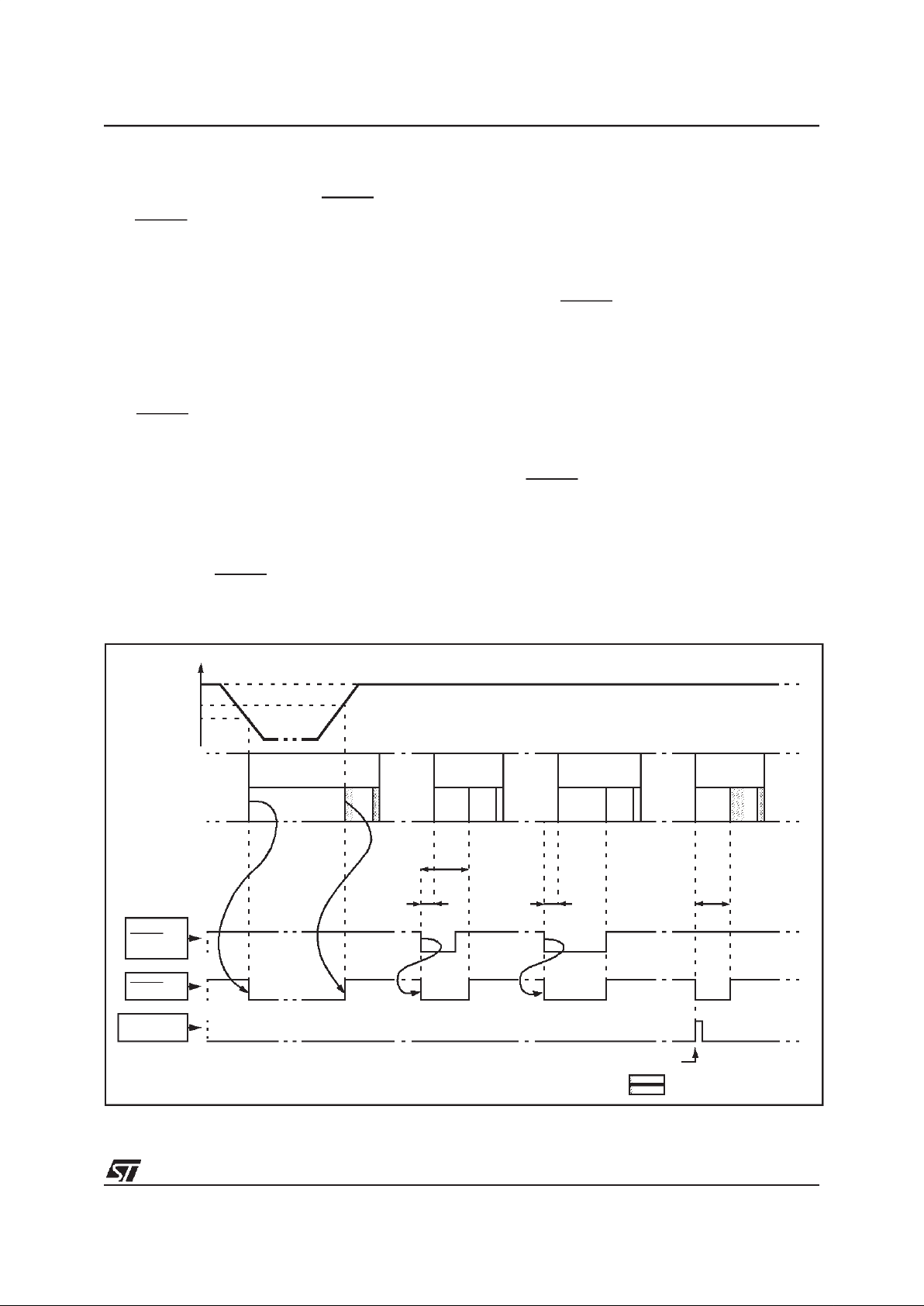
8.2 RESET SEQUENCE MANAGER (RSM)
8.2.1 Introduction
The reset sequence manager includes three RESET sources as shown in Figure 15:
■ External RESET source pulse
■ Internal LVD RESET (Low Voltage Detection)
■ Internal WATCHDOG RESET
These sources act on the RESET pin and it is always kept low during the delay phase.
The RESET service routine vector is fixed at addresses FFFEh-FFFFh in the ST7 memory map.
The basic RESET sequence consists of 3 phases
as shown in Figure 14:
■ Delay depending on the RESET source
■ 4096 CPU clock cycle delay
■ RESET vector fetch
The 4096 CPU clock cycle delay allows the oscillator to stabilise and ensures that recovery has
taken place from the Reset state.
The RESET vector fetch phase duration is 2 clock
cycles.
Figure 14. RESET Sequence Phases
Figure 15. Reset Block Diagram
RESET
DELAY
INTERNAL RESET
4096 CLOCK CYCLES
FETCH
VECTOR
f
CPU
COUNTER
RESET
R
ON
V
DD
WATCHDOG RESET
LVD RESET
INTERNAL
RESET
ST72334J/N, ST72314J/N, ST72124J
27/148
RESET SEQUENCE MANAGER (Cont’d)
8.2.2 Asynchronous External RESET pin
The RESETpin is both an input andan open-drain
output with integrated RONweak pull-up resistor.
This pull-up has no fixed value but varies in accordance with the input voltage. It can be pulled
low by external circuitry to reset the device. See
electrical characteristics section for more details.
A RESET signal originating from an external
source must have a duration of at least t
h(RSTL)in
in
order to be recognized. This detection is asynchronous and therefore the MCU can enter reset state
even in HALT mode.
The RESET pin is an asynchronous signal which
plays a major role in EMS performance. In a noisy
environment, it is recommended to follow the
guidelines mentioned in the electrical characteristics section.
Two RESET sequences can be associated with
this RESET source: short or long external reset
pulse (see Figure 16).
Starting from the external RESET pulse recognition, the device RESET pin acts as an output that
is pulled low during at least t
w(RSTL)out
.
8.2.3 Internal Low Voltage Detection RESET
Two different RESET sequences caused by the internal LVD circuitry can be distinguished:
■ Power-On RESET
■ Voltage Drop RESET
The device RESET pin acts as an output that is
pulled low when VDD<V
IT+
(rising edge) or
VDD<V
IT-
(falling edge) as shown in Figure 16.
The LVD filters spikes on VDDlarger than t
g(VDD)
to
avoid parasitic resets.
8.2.4 Internal Watchdog RESET
The RESET sequence generated by a internal
Watchdog counter overflow is shown in Figure 16.
Starting from the Watchdog counter underflow, the
device RESET pin acts as an output that is pulled
low during at least t
w(RSTL)out
.
Figure 16. RESET Sequences
V
DD
RUN
RESET PIN
EXTERNAL
WATCHDOG
DELAY
V
IT+
V
IT-
t
h(RSTL)in
t
w(RSTL)out
RUN
DELAY
t
h(RSTL)in
DELAY
WATCHDOG UNDERFLOW
t
w(RSTL)out
RUN RUN
DELAY
RUN
RESET
RESET
SOURCE
SHORT EXT.
RESET
LVD
RESET
LONG EXT.
RESET
WATCHDOG
RESET
INTERNAL RESET (4096T
CPU
)
FETCH VECTOR
ST72334J/N, ST72314J/N, ST72124J
28/148
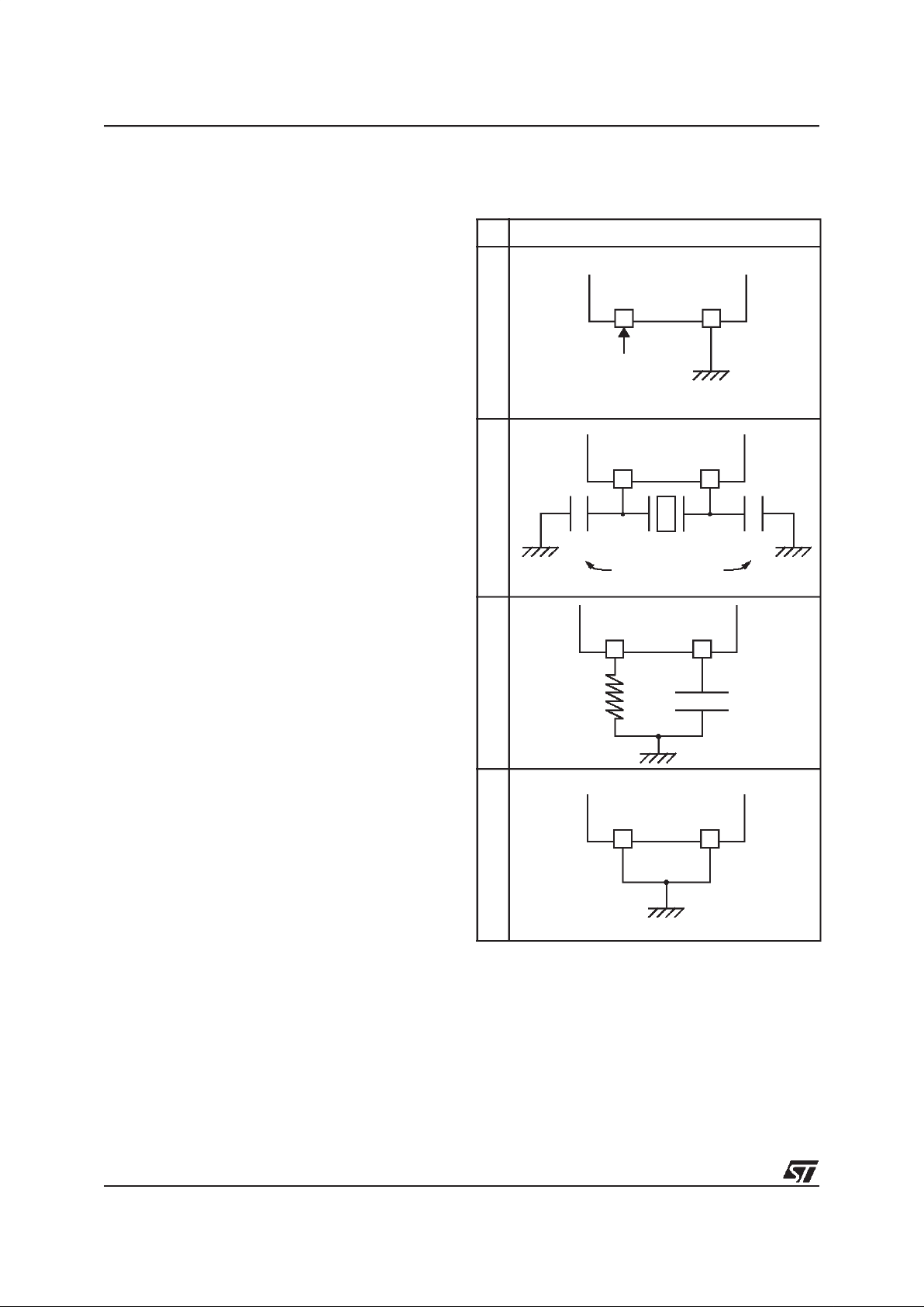
8.3 MULTI-OSCILLATOR (MO)
The main clock of the ST7 can be generated by
four different source types coming from the multioscillator block:
■ an external source
■ 4 crystal or ceramic resonator oscillators
■ an external RC oscillator
■ an internal high frequency RC oscillator
Each oscillator is optimized for a given frequency
range in terms of consumption and is selectable
through the option byte. The associated hardware
configuration are shown in Table 4. Refer to the
electrical characteristics section for more details.
External Clock Source
In this external clock mode, a clock signal (square,
sinus ortriangle) with~50% duty cycle has todrive
the OSC1 pinwhile theOSC2 pinis tied to ground.
Crystal/Ceramic Oscillators
This family of oscillators has theadvantage of producing a very accurate rate on the main clock of
the ST7. The selection within a list of 4 oscillators
with different frequency ranges has to be done by
option byte in order to reduce consumption. In this
mode of the multi-oscillator, the resonatorand the
load capacitors have to be placed as close as possible to the oscillator pins in order to minimize output distortion and start-up stabilization time. The
loading capacitance values must be adjusted according to the selected oscillator.
These oscillators are not stopped during the
RESET phase to avoid losing time in the oscillator
start-up phase.
External RC Oscillator
This oscillator allows a low cost solution for the
main clockof the ST7 using only an external resistor and anexternal capacitor.The frequencyof the
external RC oscillator (in the range of some MHz.)
is fixed by the resistor and the capacitor values.
Consequently in this MO mode, the accuracy of
the clock is directly linked to the accuracy of the
discrete components.
Internal RC Oscillator
The internal RC oscillator mode is based on the
same principle as the external RC oscillator including the resistance and the capacitance of the device. This mode is the most cost effective one with
the drawback of a lower frequency accuracy. Its
frequency is in the range of several MHz.
In this mode, the two oscillator pins have to be tied
to ground.
Table 4. ST7 Clock Sources
Hardware Configuration
External ClockCrystal/Ceramic ResonatorsExternal RC OscillatorInternal RC Oscillator
OSC1 OSC2
EXTERNAL
ST7
SOURCE
OSC1 OSC2
LOAD
CAPACITORS
ST7
C
L2
C
L1
OSC1 OSC2
ST7
C
EX
R
EX
OSC1 OSC2
ST7
ST72334J/N, ST72314J/N, ST72124J
29/148
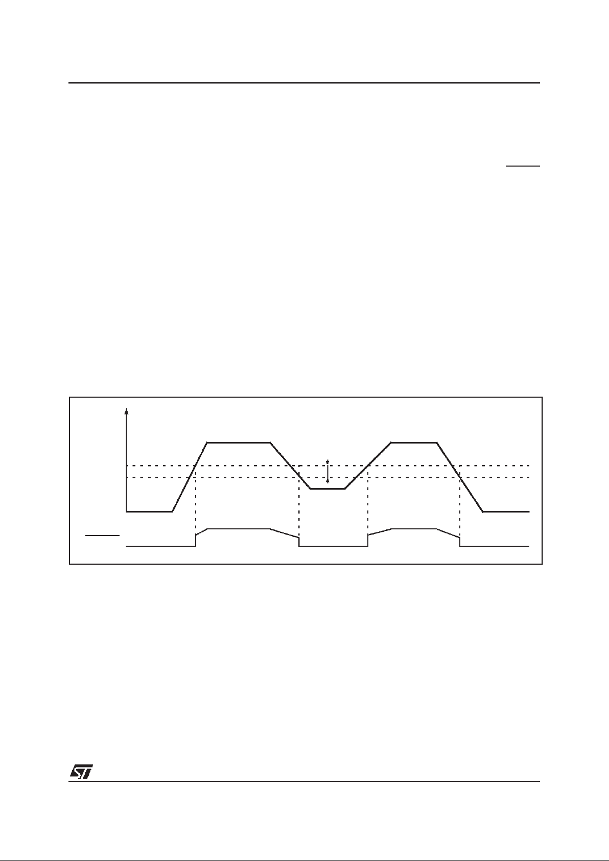
8.4 CLOCK SECURITY SYSTEM (CSS)
The Clock Security System (CSS) protects the
ST7 against main clock problems. To allow the integration of the security features in the applications, itis based on a clock filter control and anInternal safe oscillator. The CSS can be enabled or
disabled by option byte.
8.4.1 Clock Filter Control
The clock filter is based on a clock frequency limitation function.
This filter function is able to detect and filter high
frequency spikes on the ST7 main clock.
If the oscillator is not working properly (e.g. working at a harmonic frequency of the resonator), the
current active oscillator clock can be totally filtered, and then no clock signal is available for the
ST7 from this oscillator anymore. If the original
clock source recovers, the filtering is stopped automatically and the oscillator supplies the ST7
clock.
8.4.2 Safe Oscillator Control
The safe oscillator of the CSS block is a low frequency back-up clock source (see Figure 17).
If the clock signal disappears (due to a broken or
disconnected resonator...) during a safe oscillator
period, the safe oscillator delivers a low frequency
clock signalwhich allows the ST7 to perform some
rescue operations.
Automatically, theST7 clock sourceswitches back
from the safe oscillator if the original clock source
recovers.
Limitation detection
The automatic safe oscillator selection is notified
by hardware setting the CSSD bit of the CRSR
register. An interrupt can be generated if the CSSIE bit has been previously set.
These two bits are described in the CRSR register
description.
8.4.3 Low Power Modes
8.4.4 Interrupts
The CSS interrupt event generates an interrupt if
the corresponding Enable Control Bit (CSSIE) is
set and the interrupt mask in the CC register is reset (RIM instruction).
Figure 17. Clock Filter Function and Safe Oscillator Function
Mode Description
WAIT
No effect on CSS. CSS interrupt cause the
device to exit from Wait mode.
HALT
The CRSR register is frozen. The CSS (including the safe oscillator) is disabled until
HALT mode is exited.The previous CSS
configuration resumes when the MCU is
woken up by aninterrupt with “exit from
HALT mode” capability or from the counter
reset value when the MCU is woken up by a
RESET.
Interrupt Event
Event
Flag
Enable
Control
Bit
Exit
from
Wait
Exit
from
Halt
CSS event detection
(safe oscillator activated as main clock)
CSSD CSSIE Yes No
f
OSC
/2
f
CPU
f
OSC
/2
f
CPU
f
SFOSC
SAFE OSCILLATOR
FUNCTION
CLOCK FILTER
FUNCTION
ST72334J/N, ST72314J/N, ST72124J
30/148
8.5 SUPPLY, RESET AND CLOCK REGISTER DESCRIPTION
Read/Write
Reset Value: 000x 000x (xxh)
Bit 7:5 = Reserved, always read as 0.
Bit 4 = LVDRF
LVD reset flag
This bit indicates that the last RESET was generated by the LVD block. It is set by hardware (LVD
reset) and cleared by software (writing zero). See
WDGRF flag description for more details. When
the LVD is disabled by option byte, the LVDRF bit
value is undefined.
Bit 3 = Reserved, always read as 0.
Bit 2 = CSSIE
Clock security syst.interrupt enable
This bit enables the interrupt when a disturbance
is detected bythe clock security system (CSSD bit
set). It is set and cleared by software.
0: Clock security system interrupt disabled
1: Clock security system interrupt enabled
Refer to Table 6, “Interrupt Mapping,” on page 32
for more details on the CSS interrupt vector. When
the CSS is disabled by option byte, the CSSIE bit
has no effect.
Bit 1 = CSSD
Clock security system detection
This bit indicates that the safe oscillator of the
clock security system block has been selected by
hardware due to a disturbance on the main clock
signal (f
OSC
). It is set by hardware and cleared by
reading the CRSR register when the originaloscillator recovers.
0: Safe oscillator is not active
1: Safe oscillator has been activated
When the CSS is disabled by option byte, the
CSSD bit value is forced to 0.
Bit 0 = WDGRF
Watchdog reset flag
This bit indicates that the last RESET was generated by the watchdog peripheral. It is set by hardware (Watchdog RESET) and cleared by software
(writing zero) or an LVD RESET (to ensure a stable cleared state of the WDGRF flag when the
CPU starts).
Combined with the LVDRF flag information, the
flag description is given by the following table.
Application notes
The LVDRF flag is not cleared when another RESET type occurs (external or watchdog), the
LVDRF flagremains set to keep trace of the original failure.
In this case, a watchdog reset can be detected by
software while an external reset can not.
Table 5. Clock, Reset and Supply Register Map and Reset Values
70
000
LVD
RF
0
CSSIECSSDWDG
RF
RESET Sources LVDRF WDGRF
External RESET pin 0 0
Watchdog 0 1
LVD 1 X
Address
(Hex.)
Register
Label
76543210
002Bh
CRSR
Reset Value 0 0 0
LVDRF
x0
CFIE
0
CSSD0WDGRF
x
 Loading...