

ST70136
CPE ADSL ANALOG FRONT END
■ WIDE TRANSMIT AND RECEIVE DYNAMIC
RANGE TO REDUCE EXTERNAL
FILTERING REQUIREMENTS
■ RECEIVE PROGRAMMABLE GAIN: 0 TO
31dB GAIN IN 1dB STEPS
■ RECEIVE PROGRAMMABLE ATTENUATOR
0,-4dB, -8dB, -12dB
■ 12-BIT A/D CONVERTER IN RECEIVE PATH
■ TRANSMIT PROGRAMMABLE GAIN: 0 TO
-15dB IN 1dB STEPS
■
14-BIT D/A CONVERTER IN TRANSM IT PATH
■ LOW POWE R MODE: 10mW IN LISTE NING
MODE, 250
µ
W IN POWER DOWN
■ TONE DETECTOR: ACTIVITY DETECTION
FOR WAKE-UP F UNCTION
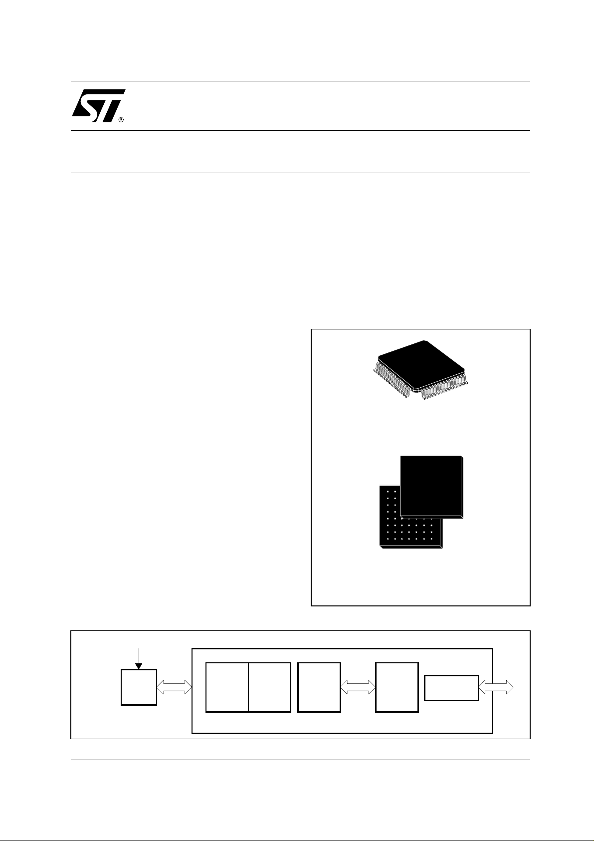
■ 64-PIN TQFP PACKAGE
■ 64-PIN L FBGA PACKAGE
■ 0.50
µ
m, 5V BICMOS TECHNOLOGY
■ 3.3V DIGITA L I NTERFACE
■ 5V ANALOG IN TERFACE
INTRODUCTION
The ST70136 ADSL Analog Front End (AFE) chip
implements the analog transceiver functions
required in a Custome r Premise ADSL m odem. It
connects the digital modem chip with the loop
driver and hybrid balance circuits.
The AFE has been designed with high dynamic
range in order to greatly reduce the external filtering requirements at the front end.
The AFE chip and its companion digital chip along
with a loop driver, implement the complete
G.992.2 and G.992.1 DMT modem solution.
The AFE receive path contains a programmable
gain amplifier (RxPGA), a low pass anti-aliasing
filter, and a 12-bit A/D converter. The RxPGA is
digitally programmable from 0 to 31dB in 1dB
steps.
The AFE transmit path consists of a 14-bit D/A
converter, followed by a programmable gain
amplifier (TxPGA). The transmit gain is programmable from 0 to -15dB in 1dB steps.
TQFP64 Fu ll Pla st i c
(10 x 10 x 1.40 mm)
ORDER CODE: ST70136G
LFBGA64
(8 x 8 x 1.7 mm)
ORDER CODE: ST70136B
Figure 1 : Overall Application Block Diagram
Software for Control xDSL
PC
PCI
or
USB
PCI
or
USB
ST70137
DMT
xDSL
AFE
ST70136
LOOP
DRIVER
TS612/TS652
LINE
HYBRID
1/24September 2001

2/24
CTRLOUT
2
47
CTRLIN
1
48
64 63 62 61 60 59 58 57 56 55 54 53 52 51 5 0 49
VDDOSC
XTALO
XTALI
VSSOSC
VSSESD
VSSA6
VCOCAP
IVCO
VCXOUT
TOP
TON
VDDA6
GC0
GC1
VDDA5
VSSA5
VSS
TEST
NRESET
VDD
PWD
SUSPEND
VDDA2
VSSA2
VSAD
VSRX
VSSA1
RXP
RXN
VDDA1
VDDA3
IREF50U
22 23 24 25 26 27 28 29 30 31 3217 18 19 20 21
TX0
16
33
TX1
15
34
TX2
14
35
TX3
13
36
VSSIO
12
37
RX0
11
38
RX1
10
39
RX3
RX2
8
9
ST70136G
41
40
ACTD
7
42
CLKM
6
43
CLKWD
5
44
VDDIO
4
45
R/W
3
46
ST70136 Pinout
ST70136
VSDA
VDDA4
PGAP
TXIN
TXP
TXN
TXIP
PGAN
VSSA4
VSSA3
V290DA
V125AD
V250AD
V375AD
VSBIAS
V3P75V

1 - PIN LIST
The following list gives the different PIN Types:
AI Analog Input
AIO Analog Input/Output
AO Analog Ouptut
DI Digital Input
DIO Digital Input/Output
DO Digital Output
VDDA Analog Power Supply
VDDD Digital Power Supply
VSSA Analog Ground
VSSD Digital Ground
Table 1 : Pin Assignment
Pins
Name Type Description
TQFP LFBGA
1 B2 CTRLIN DI Digital input for control interface
2 C3 CTRLOUT DO Digital output for control interface
3 C2 R/NW* DI Selection of read or write mode for control interface
4 B1 VDDIO VDDD I/O buffer supply voltage
5 A1 CLKWD DO 8.832MHz output clock. Used to synchronize RX/TX word data
6 C1 CLKM DO 35.328MHz Master Clock. Xtal buffer
7 D2 ACTD O Tone Detector Activation
8 D1 RX3 DO Received data output
9 E2 RX2 DO Received data output
10 E1 RX1 DO Received data output
11 F2 RX0 DO Received data output
12 G2 VSSIO VDDD I/O buffer ground voltage
13 F1 TX3 DI Transmit data input
14 G1 TX2 DI Transmit data input
15 H2 TX1 DI Transmit data input
16 H1 TX0 DI Transmit data input
17 E3 VSS VSSD Core digita l ground
18 G3 TEST DI Test mode is activated with TEST=1. Must be tied to ground in normal
19 E4 NRESET* DI Reset input. All digital circuitry is well defined after a negative pulse on
20 H3 VDD VSSD Core digital supply (3.3V)
21 F3 PWD DI Power Down pin
22 G4 SUSPEND DI Suspend Mode pin
23 F4 VDDA2 VDDA ADC supply voltage (5V)
24 H4 VSSA2 VSSA ADC ground voltage
25 G5 VSAD VSSA Substrate voltage for RX-AD path (Must be connected to VSSAx)
26 E5 VSRX VSSA Substrate voltage for RXPGA path (Must be connected to VSSAx)
27 H5 VSSA1 VSSA RXPGA ground voltage
28 H6 RXP AI Positive Analog Receive input
exchange, and master clock of register control interface
mode
this input
ST70136
3/24

ST70136
Table 1 : Pin Assignment (continued)
Pins
Name Type Description
TQFP LFBGA
29 H7 RXN AI Negative Analog Receive input
30 G6 VDDA1 VDDA RXPGA voltage supply (5v)
31 F5 VDDA3 VDDA Bias and References voltage supply (5v)
32 H8 IREF50U AI External resistor for bias current 50kΩ
33 G8 V3P75V AO 3.75v output from bandgap; 0.22µF decoupling
34 G7 VSBIAS VSSA Substrate voltage for biasing & reference cell (Must be connected to
35 F7 V375AD AO 3.75 volt reference voltage. Need decoupling 0.1µF
36 F8 V250AD AO 2.50 volt reference voltage. Need decoupling 0.1µF
37 F6 V125AD AO 1.25 volt reference voltage. Need decoupling 0.1µF
38 E7 V290DA AO 2.90 volt reference voltage. Need decoupling 0.1µF
39 E8 VSSA3 VSSA Biasing and References ground voltage
40 E6 VSSA4 VSSA Tx path ground voltage
41 D6 PGAN AO Negative TXPGA output
42 D8 TXIP AI Positive analog input for Tx external filtering
43 D7 TXN AO Negative analog transmit output
44 C7 TXP AO Positive analog transmit output
45 C8 TXIN AI Negative analog input for Tx external filtering
46 B7 PGAP AO Positive TXPGA output
47 B8 VDDA4 VDDA Tx analog supply voltage (5V)
48 A8 VSDA VSSA Substrate voltage for DAC path (Must be connected to VSSAx)
49 A7 VSSA5 VSSA DAC path ground voltage
50 C6 VDDA5 VDDA DAC analog supply voltage (5v)
51 A6 GC1 DO MSB for external gain control
52 B6 GC0 DO LSB for external gain control
53 D5 VDDA6 VDDA VCXO & Tone detector Input analog supply voltage (5v)
54 C5 TON AI Negative tone detector input
55 B5 TOP AI Positive tone detector input
56 D4 VCXOUT AIO VCXO output current
57 A5 IVCO AIO VCXO input current
58 C4 VCOCAP AO VCXO output filtering
59 A4 VSSA6 VSSA VCXO & Tone detector analog ground voltage
60 B4 VSSESD VSSD Ground voltage reference for ESD
61 D3 VSSOSC VSSD Ground voltage for Xtal oscillator
62 A3 XTALI DI Xtal oscillator input
63 B3 XTALO DO Xtal oscillator output
64 A2 VDDOSC VDDD Supply voltage for Xtal cell (3.3v)
VSSAx)
* A "N" me ans active low. Example: R/NW means write active low.
4/24

2 - PIN DESCRIPTION
ST70136
2.1 - Analog Power Supplies
These pins are the posit ive analog power supply
voltage for the DAC and the ADC section. It is not
internally connecte d to digital supply. In any case
the voltage on these pins m ust be hi gher or equa l
to the voltage of the Digital power supply.
2.2 - Digital Power Supplies
These pins are the power supply pins that are
used by the internal digital circuitry. All DVDD pins
must be connected together to a +3.3 V supply.
2.3 - Anal og Gr ound and Substr at e
These pins are the ground return of the analog
DAC and ADC blocks. The analog VDDA shoul d
be decoupled with respect to the analog ground.
Decoupling capacitors should be as close as pos sible to the supplies pins. All grounds must be tied
together.
2.4 - Digita l Ground
These pins are the ground ret urn of the di gital circuitry. The digital p ower supplies must shou ld be
decoupled with respect to the digital ground.
Decoupling capacitors should be as close as pos sible to the supplies pins. All grounds must be tied
together.
2.5 - Powerd own - PWD
When pin PWD =”1”, the chip is set in low power
mode.
2.6 - Suspend
The SUSPEND pin is used to control the output of
CLKM. When SUSPEND is low CLKM output is
enabled otherwise CLKM is disabled.
2.8.2 - V3P75V
This pin is the 3.75V Bandgap output and shoul d
be externally decoupled with an external capacitor
of 0.22uF.
2.8.3 - IREF50U
This pin is used for s etting the bias current and
must be externally connected to a resistor of
2.5V / 50
µ
A equals 50kΩ.
2.8.4 - V290DA
This pin is the 2.9V transmit DAC output reference
voltage and must be decoupled externally.
2.9 - Analog Transmit Output
2.9.1 - TXP
This pin is t he n on-invert ing out put of t he full y dif ferential analog amplifier.
2.9.2 - TXN
This pin is the inverting output of the fully differential analog amplifier.
2.9.3 - TXIP
This pin is the d ifferential non-inverting input for
external filtering.
2.9.4 - TXIN
This pin is the di fferential inverting input f or e xternal filtering.
2.9.5 - PGAP
This pin is the differential non-inverting PGA output.
2.9.6 - PGAN
This pin is the differential inverting PGA output.
2.10 - An alog Rece ive Input
2.7 - Reset
The reset function is implied when the NRESET
pin is at a low voltage input level. In this condition,
the reset function can be easily used f or power up
reset conditions. Reset is asynchronous, tenths of
ns are enough to put the IC in reset. After reset, all
registers are set to their default value.
2.8 - Reference Voltages
2.8.1 - V125AD, V250AD, V375AD
These pins are used to externally decouple the
internal reference voltages used for the ADC
(1.25V, 2.5V, 3.75V).
2.10.1 - RXN
This pin is the differential inverting receive input.
2.10.2 - RXP
This pin is the differential non-inverting receive
input.
2.11 - Tone Detector
The analog input differential signal must be less
than 8V peak to peak. These pins are used for
activity detection when in sleeping mode.
2.11.1 - TON
This pin is the differential inverting tone d etector
input.
5/24

ST70136
2.11.2 - TOP
This pin is the differential non-inverting tone
detector input.
2.11.3 - ACTD
This pin is active when t one 40 or 72 has been
detected in sleeping mode (see control register)
2.12 - CRYSTAL
These pins must be tied to an external crystal
(F = 35.328MHz).
2.12.1 - XTAL I
This pin is the crystal os cillat or input .
2.12.2 - XTAL O
This pin is the c r yst a l os c illa t or ou t pu t.
2.13 - VCXO
2.13.1 - IVCO
This pin is the current reference for the VCO DAC
2.13.2 - VCOCAP
This pin is used to introduce time constant. The
tuning is done by connecting an external capacitor
2.13.3 - VCXOUT
This pin is the output control current generated by
a 8 bit DAC.
2.14 - Control Serial Interface
Access to the cont rol register c an b e done only in
stable state fonctionality:
SUSPEND = "0".
2.14.1 - CTRLIN
This pin is used to program the internal registers.
The data burst is c omp osed of 16 bits sampled at
CLKM when CL KWD = 1. The first bit is used as
start bit (’0’), the three LSBs being used to identify
the data contained in the twelve remaining bits.
The start bit b15 (b5 = 0) is transmitted first followed by bits b[14:0]. At leas t 1 stop bit "1" need
to be provided to validate the data.
2.14.2 - CTRLOUT
This pin is the con trol register output. The burst
data on this pin is the value of the register
addressed by CTRLIN.
2.14.3 - CLKWD
This pin is the word clock used to sample the control information and equal to CLKM / 4.
2.14.4 - R/NW
This pin is used for the read and write operation
for the control interface and sampled at the s ame
time than bit b15 of CTRLIN.
2.14.5 - Digital Interface
The interface is a nibble serial interface running at
8.832MHz sampling frequency. The data are presented in 16bits format, and transferred in groups
of 4 bits (nibbles). The LSBs are transferred first.
Data is transmitted on the rising e dge of the m aster clock CL KM
2.14.6 - CLKM
This pin is the master c lock equal to 35.328MHz
and is the sampling clock of the input / output
data.
2.14.7 - TX0, TX1, TX2, TX3
These pins are the digital transmit data input.
2.14.8 - RX0, RX1, RX2, RX3
These pins are the digital receive data output.
2.15 - Test
This pin is dedicated to put the ST70136 i n test
mode.
6/24

3 - BLOCK DIAGRAM
XTALI XTALO
62
63
TEST
18
SUSPEND
22
PWD
21
V125AD
37
V250AD
36
V375AD
35
V290DA
38
ST70136
V3P75V IREF50U
33 32
TX0
TX1
TX2
TX3
CLKM
RX0
RX1
RX2
RX3
CLKWD
ACTD
CTRLIN
CTRLOUT
R/NW
NRES ET
16
15
14
13
6
11
10
9
8
5
7
1
2
3
19
INTERNAL
VCXO
CLOCK
GENERATOR
1
1
1
1
INTERFACE
1
1
1
1
CONTROL
INTERFACE
DATA
MANAGEMENT
16
16
8
POWER
14-BIT
DAC
8-BIT
DAC
12-BIT
ADC
AAF
TONE
DETECTOR
BANDGAP
REFERENCE
+-
PA
+-
TxPGA
RxPGA
ATT
42
43
44
45
41
46
29
28
54
55
52
51
56
TXIP
TXN
TXP
TXIN
PGAN
PGAP
RXN
RXP
TON
TOP
GC0
GC1
VCXOUT
58
VCOCAP IVCO
57
7/24

ST70136
4 - FUNCTIONAL DESCRIPTION
4.1 - General
The ST70136 consists of the following functional
blocks:
– Transmit Signal Path
– Receive Signal Path
– Bias Voltage and Current Generation
– Digital Data Interface
– Control Serial Interface
– Tone Detector
– Power Down m ode ma nagem ent
4.2 - Transmit Path Description
The transmit path contains the 14-bit digital to
analog converter (DAC) necessary to generate
the transmit signal from a 16-bit digital input word.
This transmit signal is then scaled by the on chip
programmable gain amplifier (TxPGA) from 0 to
-15dB in 1dB s teps. The scaled output signal is
then driven off chip to the external filters and
power amplifier (PA) which drives the DMT signal
to the subscriber loop. The transmit path is fully
differential.
4.3 - Receive Path Description
The receive path contains first an attenuator
(which allows the selection between 4 at tenuated
versions of the signal) followed by a program mable gain amplifier (RxPGA), a 1st order low pass
anti-aliasing filter, and a 12-bit analog to digital
converter (ADC). The RxPGA gain is digitally programmable from 0 to 31dB in 1dB steps. The
receive path is fully differential.
4.4 - VCXO
The ST70136 contains the circuits required to
construct an internal VCXO. It is divided in a crystal driver and an auxiliary 8 bits DAC for timing
recovery. The crystal driver is able to operate at
35.328MHz.
The DAC which is driven by the CTRLIN p in (the
input of the Serial Control Interface), provides a
current output with 8 bits resolution and can be
used to tune the crystal frequency with the help of
external components. A time constant between
DAC input and VCXOUT can be introduced (via
CTRLIN interface) and p rogram med with the hel p
of an external capacitor (on VCOCAP pin).
4.5 - Bias Voltage and Current Generation
The bias circuitry c ontains a bandgap voltage reference from which the converters references a nd
analog ground voltages are generat ed. This block
also generates a n a ccurate bias current us ing an
external resistor.
4.6 - Digital Data Interface
To facilitate data transfer between the ST70136
and the digital data pump, a 4-bit wide serial interface for the trans mit and receive path is incorporated into the AFE.
This interface consists of four transmit pins
(TX[0:3]), four receive pins (RX[0:3]), and the necessary control signals (CLKM, CLK WD) to transmit and receive the required data.
8/24

Figure 2 : Digital Data Interface
CLKM
35.328MHz
CLKWD
8.832MHz
ST70136
TX[0]/RX [0]
TX[1]/RX [1]
TX[2]/RX [2]
TX[3]/RX [3]
TX DA TA
RX DATA
a0
a1
a15 a0
Sign DATA..................................................................................LSB
a15
Sign Sign DAT A .................................................................... 0 0 0
a14 a13
a12a8a4
a13a9a5
a14a10a6a2
a15a11a7a3
4.7 - Control Serial Interface
There is a 4-pin serial digital interface (CLKWD,
CTRLIN, CTRLOUT, R/W) that access one of the
8 x 12-bit registers that controls all the programmable features on the ST70136.
The registers are loaded with the asynchronous
type data burst delivered to CTRLIN pin. It is com-
a2a14 a13 a0a1
posed of 16 bits from which the first bit (b15) is
used as start bit (‘0’), the three LSBs (b2:b0) being
used to identify the register to be loaded.
The twelve remaining bits (b14:b3) are the control
data. During a read operation, the CTRLO UT pin
figures out the register contents addressed by
CTRLIN pin.
Figure 3 : Control Register Interface Write Cycle
CLKM
CLKWD
b15
CTRLIN
CTRLOUT
R/NW
Data for write access [b14:b3] [b2:b0]
9/24

ST70136
Figure 4 : Control Register Interface Read cycle
CLKM
CLKWD
b15
CTRLIN
CTRLOUT
R/NW
Don’t care [b2:b0]
b15
Data [b14:b3]
4.7.1 - AFE registers
4.7.1.1 - Rx Gain Control
This register is located at the address “000” and is used to program the gain in the receive path.
Table 2 : Rx Gain Control (address [b2:b0]=”000”)
Name Pos. Type Def. Description
GC[1:0] 14.13 R/W 00 bit14: selects External Gain Control
Other 12 R/W 0 Reserved
RxAGC 11..7 R/W 00000 Select internal gain for Receive amplifier
RxAtt 6..5 R/W 00 Receive attenuator
Other 4.3 R/W 00 Reserved
GC1
bit13: selects External Gain control
GC0
00000 : 0dB
11111 : 31dB
00 = 0dB
01 = -4dB
10 = -8dB
11 = -12dB
4.7.1.2 - Tx Gain Control
This register is located at the address “001” and is used to program the gain in the transmit path.
Table 3 : Tx Gain Control (address [b2:b0]=”001”)
Name Pos. T ype Def. Description
TxAGC 14..11 R/W 0000 Select internal gain for Transmit amplifier
0000 : -15dB
1111 : 0dB
Other 10..3 R/W 0..0 Reserved
10/24

4.7.1.3 - Special Features Configuration
This register is located at the address “010” and is used to configure different blocks.
Table 4 : Adsl Configuration (address [b2:b0]=”010”)
Name Pos. Type Def. Description
Reserved 14.13 R/W 00 Reserved
VCO-DAC 12 R/W 1 Enable the VCO DAC
1: enabled
0: disabled
Other 11.4 R/W 0..0 Reserved
FVCXO 3 R/W 0 Filtered VCXO output
1 : filtered
0 : not filtered
4.7.1.4 - VCXO Control
Table 5 : VCXO DAC Value (address [b2:b0]=”011”)
Name p os. type def. Description
DAC value 14..7 R/W 80H 8 bits for VCO DAC.
0...0 = min. current
1...1 = max current.
Others 6..3 R/W 0000 Reserved
ST70136
4.7.1.5 - Test On ly Register s
They are presently located at address “100” to “101”.
4.7.1.6 - To ne Detecti on Threshold Setting Register
Table 6 : Tone Detection Threshold Setting Register (address [b2:b0]=”110”)
Name Pos. Type Def. Description
Threshold Level 14..5 R/W 1000000000 Set the threshold of the tone detector
Reserved 4.3 R/W 00 Reserved
4.7.1.7 - Status Register & tone detector
This register can be used in the case of read / write registers.
Table 7 : Status & Tone Detector Register (address [b2:b0]=”111”)
Name Pos. Type Def. Description
Receiver Clip indicator 14
Transceiver Clip indicator 13 R/W_clear 0 1: Transmit Clipping occurred
Sleeping Mode 12 R/W 0 0: disable tone detector in power down
Tone Detector 11 R/W 0 Tone detector frequency setting
Debug Mode 10 R/W 0 When in normal mode “0” the CTRLOUT pin is in HIZ
Software Reset 9 R/W 0 When set all registers are set to their default value
Reserved 8..3 R/W 0..0 Reserved
Note: 1. R/W_clear: bit is resetted to 0 by writing 0.
R/W_clear
1
0 1: Receive Clipping occurred
1: enable tone detector in power down
0: standard ADSL (tone 40)
1: ADSL over ISDN (tone 72)
and don’t care for R/W and the control access register
are always writing operation whatever on R/W pin.
When in debug mode “1” the CTRLOUT and R/W pins
are operating as defined in pin description chapter.
11/24

ST70136
4.8 - Tone Detector
The tone detecto r is dedicated for rem ote a ctivation. It operates d uring SUSPE ND mode with P WD = 0
only. When the tone detector level received Vin over tone 40 or 72 is greater than 15
ACTD pin is set to wake up the modem.
ACTD pin is resetted when the AFE is back in full operating mode (SUSPEND = 0, PWD = 0). The maximum signal sensitivity at the Tone dete ctor inputs is 50mV peak to peak.
4.9 - Mode Management
4.9.1 - General
The ST70136 can be used in a various range of ATU-R equipments, but a specific mode ma nagement
address USB application in its different modes.
In following table, "CPE" is an USB ADSL modem application done with a ST70136 AFE and a ST70137
DMT. The CPE is connected to an USB port of an equipment.
Table 8 : ST70136 / USB Operating Mode Configurations
SUSPEND PWD USB Mode Description
00Active mode
The CPE application is in operative mode, its current consumption is less than 500 mA.
ST70136 is power-up, the Tone detector is OFF and CLKM output is enabled.
01Enumerating mode
The CPE application is in the configuration process, plug in, its current consumption is
less than 100 mA.
ST70136 analog part is in power done mode, the digital part is enabled and CLKM
output is enabled.
10Suspend mode after enumerating mode
After enumerating, the CPE application is in suspend mode, in this mode the CPE must
be able to wake up the equipment when a tone is received, its current consumption is
less than 2.5 mA.
ST70136 analog and digital parts are in power down mode, the Tone detector is
activated and CLKM output is disabled.
11Stand by mode
The CPE is not configured and in stand by mode, it could be wake up only by the
equipment, its current consumption is less than 500µA.
ST70136 is fully in stand by mode and CLKM is disabled.
µ
V peak to peak, the
Figure 5 : USB Power Management Operating Modes
Plug in
Enumerating mode
PWD = 1
SUSPEND = 0
Stand by mode
PWD = 1
SUSPEND = 1
12/24
Suspend mode
PWD = 0
SUSPEND = 1
Active mode
PWD = 0
SUSPEND = 0

4.9.2 - Reset Timing
Figure 6 : Reset Timing
V
VDD
XTAL
ST70136
t
7ms max
5ms max
Reset
CLKM
CLKWD
SUSPEND
After CLKM depends on SUSPEND, PWD pin status
5ms done by an external R/C network
Internal counter
2ms
4.9.3 - Mode Management Timing
Figure 7 : Mode Management
Tone detector: Disabled Enabled
7ms max
XTAL
CLKM
SUSPEND
PWD
Stand by mode Enumerating mode Active mode Suspend mode
13/24

ST70136
5 - SPECIFICATIONS
5.1 - Absolute Maximum Ratings
Supply Voltage(AVDD,DVDD) -0.3V to 6V
Input Voltage -0.3V to AVDD,DVDD + 0.3V
Input current per pin -10mA to + 10mA
Output current per pin -20mA to + 20mA
Storage Temp erature -65°C to 150°C
ESD Protection 2000V
General DC Specification
Parameter Minimum T ypical Maximum Unit
AVDD 4.75 5 5.25 V
DVDD 3 3.3 3.6 V
- Active
- Listening
- Stand by
Analog
Digital
Oscillator
Analog
Digital
Oscillator
Analog
Digital
Oscillator
75
10
2
10
1.1
0.6
10
10
5
85
30
5
11
1.7
1
11
25
25
mA
mA
mA
µA
mA
mA
µA
µA
µA
5.2 - Characteristics for Digital Signals
T
= 0 to 70°C unless otherwise specified.
A
Parameter Type Conditions Minimum Typical Maximum Unit
Iil Low level input current DI Vi = 0v -1 1 µA
Iih High level input current DI Vi = VDD -1 1 µA
Ioz Tri-state output leakage DIO Vo = 0v or VDD -1 1 µA
Vih Input high voltage DI, DIO 0.8 x VDD V
Vil Input low voltage DI, DIO 0.2 x VDD V
Voh high level output voltage DO Ioh = 2mA 0.4 V
Vol low level output voltage DO Iol = 2mA 0.85 x VDD V
Col Output load capacitance DO 20 pF
14/24

ST70136
5.3 - Receive Path Specifications
TA = 0 to 70°C unless othe rwise specified. The following specifications are guaranteed only when the
Digital Contro l Interface is not active.
Table 9 : Receive Path Specifications
Typical specifications apply for VCC = 5.0V, temperature = 27°C, nominal process and bias current. Maximum and
minimum performance is with VCC ±5%, 0°C < T
Description Min. Typ. Max. Unit Comments
Output word rate 8.832 MHz Data Sampling frequency
Output word resolution 16 bits 16 bits
Reference Input signal
a
-0.8 -0.4 0 dBfs Fref=138KHz, PGA gain=0dB, Vin = 0dBr
Common mode voltage 2.4 2.5 2.6 V Measured on each single input
Differential Input impedance 12 20 28 kΩ Between RXN and RXP
Input noise
Gain, 0 ≤ D ≤ 31
b
c
D-0.5 D D+0.5 dB Receive Programmable gain. D is the
Step size 1dB
Step size 0.8 1 1.2 dB
Attenuator 0 >= Att >= -3
d
4*Att-0.5 4*Att 4*Att+0.5 dB Receive attenuator ATT is the binary
Step size 4dB
Att step size 3.5 4 4.5 dB
AAF cutoff frequency 1 1.4 2 MHz -3dB corner vs low frequency
Output SDR
2 tones
e
66 dBc
< 70°C, and worst case process and bias current.
ambient
(2.4Vpd)
15 @gain=+31dB, frequency>138KHz
nV
----------- Hz
binary value of the control word. (see
Section 4.7.1.1 - Rx Gain Control on
page 10
value of the control word. (see Section
4.7.1.1 - Rx Gain Control on page 10
For RxPGA gain=31dB, measured at
output of ADC.
Notes: a. The corres po ndin g ty pical valu e c orre sp ond t o a 2.4Vp d a t RX N/R XP diff erent iel i nput s. The 2.4V pd c or respo nd to w hat w ill be
called 0dBr for the other specifications in the present table. Variations include process, tem perature and pow er variations.
b. The inpu t nois e must be me asur ed in the f reque ncy domain from 13 8KHz t o 1.1MHz , with an sinus oidal i nput sign al at -6 0dBr
amplitud e. Frequency of th e i nput signal is 552 KH z.
c. D is the gai n relatively to the 0dBr previou sl y defined. Variati ons include process, temperature and powe r variations.
d. Monoto ni city is guaranted for RxPGA, Attenuator, but separatly.
e. Ratio between max peak amplitude of one of the 2 single tones to any spurious measured in the down-stream band
[138KHz-1.1MHz] ; each tone amplitude is at -6-31=-37dBr. The couples are (f1,f2) = (200KHz, 300KHz), (400KHz, 500KHz),
(600KHz, 700KHz).
15/24

ST70136
5.4 - Transmit Path Specifications
TA = 0 to 70°C unless othe rwise specified. The following specifications are guaranteed only when the
Digital Contro l Interface is not active.
Table 10 : Transmit Path Specifications
Typical specifications apply for VCC = 5.0V, temperature = 27°C, nominal process and bias current. Maximum and
minimum performance is with VCC ±5%, 0°C < T
Description Min. Typ. Max. Unit Comments
Input word rate 8.832 MHz
Input word resolution 16 bits
PGAP/PGAN OUTP UT
Common mode voltage 2.4 2.5 2.6 V Measured on each output
Load resistance 500 Ω Single ended
Load capacitance 10 pF Single ended
Output Impedance 1 5 Ω Single ended
Reference Output signal
a
-5% 2.4 +5% Vp Differential output @0dB gain for TxPGA
Output noise 45 See also mask diagram below ("Final
Cutoff frequency 4 MHz @-3d B
Gain,0 ≤ D ≤ 15
b
-D-0.5 -D -D+0.5 dB Programmable attenuator.
step size 1dB
Step size 0.8 1 1.2 dB
TXP/TXN OUTPUT
Common mode voltage 2.4 2.5 2.6 V Measured on each output
Load resistance 500 Ω Single ended
Load capacitance 10 pF Single ended
Output Impedance 1 5 Ω Single ended
Output SDR
2 tones ADSL/POTS
2 tones ADSL/ISDN
c
d
79
71
< 70°C, and worst case process and bias current.
ambient
nV
----------- PGAP/N noise mask")
Hz
dB For TxPGA gain = 0dB
Notes: a. This will represen ts the 0dBr for the othe r spe cificat ions in t he pres ent tab le. The level is mesur ed for the frequ ency of 30KHz
which will correspond to the reference frequency. Variations include process, temperature and power variations.
b. This gain i s given relatively to the 0dBr prev i ously defined. Varia tions include process, temperat ure and power var i ations.
c. Ratio between max peak amplitude of one of the 2 si ngl e tones to any spurious . Measure pe rf ormed for a dual tone signal (each
tone with an am plitude equal t o -6dBr), in range 30KHz to 1MHz (couple (f1,f2) are (70KHz, 80KH z), (120KHz, 13 0K Hz)).
d. Ration between max peak amplitude of one of the 2 single tones to any spurious. Measure performed for a (250KHz, 260KHz) dual
tone signal (each tone with an amplitude equal to -6dBr), in range 30KHz to 1MHz.
16/24

Figure 8 : Tone Detector Schematic
ST70136
VDDA6
TOP (PAD)
ACTD
(PAD)
All cells are supplied with VDD except ESD diodes
G
VDDA6
TON (PAD)
Table 11 : Tone DetectorSpecifications
Description Minimum Typical Maximum Unit Comments
Zin listening mode 3.5 5 6.5 kΩ Diffferential
Zin normal mode 350 500 650 kΩ Diffferential
Minimum differential input signal 15 µVp Peak to peak
Maximum diffential input signal VDD In listening mode
VCM input VDD/2 In listening mode
5.5 - VCXO
Unless otherwise noted, typical specifications apply for AVdd = 5.0V, DVdd = 3.3V, temperature = 27°C.
A voltage controlled crystal oscillator is integrated in ST70136 . Its nom inal frequency is 35.328M Hz . The
quartz crystal is connected between XTALI and XTALO pins.
Figure 9 : DAC VCXO Schematic
VCO<7:0>
(from internal
register)
DIGITAL
ANALOG
VREF
IVCO (PAD)
PMOS
VCXOUT
(PAD)
VCOCAP(PAD)
17/24

ST70136
TA = 0 to 70°C unless otherwise specified.
Table 12 : DAC 8B Specifications
Typical specifications apply for VCC = 5.0V, temperature = 27°C, nominal process and bias current. Maximum and
minimum performance is with VCC ±5%, 0°C < T
Description Minimum Typical Maximum Unit Comments
Number of bit 8
Sampling rate 1 KHz
DNL
INL
max code (FFh)
mid code (80h)
min code (00h)
Offset IVCO vs VCOCAP
a
a
-2 2 LSB
a
2.42 2.52 2.62 V
a
3.57 3.63 3.69 V
a
4.74 4.77 4.80 V
b
-0.5 0.5 LSB
-10 10 mV
Offset variation with current -20 20 mV Iout variation from 10µA to 400µA,
VCOCAP Zout
VCOCAP Zout
c
d
320 500 680 kΩ
350 500 650 Ω
VCOCAP load 10 µF
< 70°C, and worst case process and bias current.
ambient
@ code max, VCXOUT = 2.4V
Notes: a. Measured at V COCAP output, filter disabled.
µ
b. Filter disabled, current through IVCO = 10
c. Filter en abl ed.
d. Filter disabled.
A, VCXOUT = 2V.
5.6 - Crystal
Table 13 : Crystal Parameters
Parameter Symbol Minimum T ypical Maximum Unit
Start up time T
SU
Clock Frequency CLKM 35.328 MHz
Frequency adjustment range X
Note: Recom m ended Crystal: M ELCOM 35.328MHz / UM1/ 30 / 30 / 0+70 / 15pF / FUND.
ADJ
-100 100 ppm
7ms
18/24

5.7 - Data and Control Timing Interface
= 0 to 70°C unless otherwise specified.
T
A
Figure 10 : Data and Control Timing Interface
CLKM
Tc
CLKWD
Tva
RX[0:3]
TX[0:3]
Tc
ST70136
To
Ts
CTRLIN
CTRLOUT
R/NW
Symbol Description Minimum Typical Maximum Unit
Tva Data valid time
Ts Data setup time
Th Data hold time
Tc Word clock delay 0 4 ns
Fo CLKM Frequency 35.328 MHz
CLKM clock duty cycle 40 60 %
To CLKM period 28.3 ns
Th
Tva
Ts
Ts Th
04ns
13 ns
2ns
Th
19/24

ST70136
Figure 11 : Application Schema tic ST701 36
20/24

Figure 12 : CPE Application Synoptic
RRxx ppaatthh
77 tthh
33 rrdd
LLii nnee
TTrr aa nnssffoo&&CC
2200 KK hhzz
AADDSSLL // PPOO TTSS
55 tthh
LLii nnee
TTrr aa nnssffoo&&CC
111100 KKhhzz
AADDSSLL // IISSDDNN
116688 KKhh zz
RR HHyybbrriidd
TTSS66 33 44
TTxx ppaatt hh
RRxx ppaatt hh
77 tthh
330000 KKhhzz
RR HHyybbrriidd
TTSS66 33 44
TTxx ppaatthh
TTSS66 33 66
22 nndd
113388 KKhhzz
TTSS66 33 66
33 rrdd
221100 KKhhzz
ST70136
22 nndd
11..33 MMhhzz
SSTT770011 33 66
11 sstt
113388 KKhhzz
SSTT770011 3377
44 tthh
113388 KKhhzz
22 nndd
11..33 MMhhzz
SSTT770011 33 66 SS TT7700113377
11 sstt
221100 KKhhzz
44 tthh
221100 KKhh zz
CCPPEE AApppplliiccaattii oonn ss yynnooppttii cc
21/24

ST70136
6 - PACKAGE MECHANICAL DATA
Figure 13 : Package TQFP64 Full Plastic (10 x 10 x 1.40 mm)
64 49
1
e
48
E3
SEATING PLANE
E
E1
A
A2
A1
0,10 mm
.004 inch
B
16
17 32
D3
33
c
D1
D
L1
L
0,25 mm
.010 inch
K
Millimeters Inches (approx)
Dimensions
Minimum Typical Maximum Minimum Typical Maximum
A 1.60 0.063
A1 0.05 0.15 0.002 0.006
A2 1.35 1.40 1.45 0.053 0.055 0.057
B 0.17 0.22 0.27 0.007 0.009 0.011
C 0.09 0.20 0.004 0.008
D 12.00 0.472
D1 10.00 0.394
D3 7.50 0.295
e 0.50 0.0197
E 12.00 0.472
E1 10.00 1 0.394
E3 7.50 0.295
L 0.45 0.60 0.75 0.018 0.024 0.030
L1 1.00 0.039
K 0° (Minimum), 7° (Maximum)
GAGE PLANE
22/24

7 - PACKAGE MECHANICAL DATA
Figure 14 : Package LFBGA64 (8 x 8 x 1.7 mm)
ST70136
BALL 1 IDENTIFICATION
87654321
A
B
C
D
E
F
G
H
e
D1
φ
A
f
f
E1
b (64 PLACES)
A2
0.15
D
A1
Millimeters Inches (approx)
Dimensions
Minimum Typical Maximum Minimum Typical Maximum
A 1.700 0.067
A1 0.350 0.400 0.450 0.014 0.016 0.018
A2 1.100 0.043
b 0.500 0.20
D 8.000 0.315
D1 5.600 0.220
e 0.800 0.031
E 8.000 0.315
E1 5.600 0.220
f 1.200 0.047
E
23/24

ST70136
Information furnished is bel ieved to be accurate and reliable. However, STMicroe lectronics assumes no responsibility for the
consequences of use of such information nor for any infringement of patents or other rights of third parties which may result from
its use. No li cense is granted by implication or otherwise under any patent or patent rights of STMicroelectronics. Specifications
mentioned in this publication ar e subject to change without notice. This publication supersedes and replaces all information
previously supplied. S TMicroelectronics products are not authorized for use as critica l components in life suppo rt devices or
systems without express written approval of STMicroelectronics.
The ST logo is a registered trademark of STMicroelectronics
© 2001 STMicroelectronics - All Rights Reserved
STMicroele ct ronics GROUP OF COMPA NI E S
Australia - Brazil - Can ada - China - Finla nd - France - Germa n y - Hong Kong - India - Israel - Italy - Japan - Malaysia - M al ta - Morocco
Singapor e - Spain - Sweden - Switzerland - Unit ed Kingdom - United States
http://www.st.com
24/24
ST70136.REF
 Loading...