

SGS Thomson Microelectronics ST62T85BQ6, ST62E85BG1, ST6285BQ6, ST6285BQ1, ST6285B Datasheet

August 1999 1/76
Rev. 2.5
ST62T85B/E85B
8-BIT OTP/EPROM MCU WITH LCD DRIVER,
EEPROM AND A/D CONVERTER
■ 3.0 to 6.0V Supply Operating Range
■ 8 MHz Maximum Clock Frequency
■ -40 to +85°C Operating Temperature Range
■ Run, Wait and Stop Modes
■ 5 Interrupt Vectors
■ Look-up Table capability in Program Memory
■ Data Storage in Program Memory:
User selectable size
■ Data RAM: 192 bytes
■ Data EEPROM: 128 bytes
■ User Programmable Options
■ 12 I/O pins, fully programmable as:
– Input with pull-up resistor
– Input without pull-up resistor
– Input with interrupt generation
– Open-drain or push-pull output
– Analog Input
■ 4 I/Olinescan sink up to 20mA todrive LEDs or
TRIACs directly
■ One 8-bit Timer/Counter with 7-bit
programmable prescaler
■ One 8-bit Autoreload Timer/Counter with 7-bit
programmable prescaler and output compare
■ Digital Watchdog
■ 8-bit A/D Converter with 8 analog inputs
■ 8-bit Synchronous Peripheral Interface (SPI)
■ 8-bit AsynchronousPeripheralInterface (UART)
■ LCD driver with 40 segment outputs, 8
backplane outputs, 8 software selectable
segment/backplane outputs and selectable
multiplexing ratio.
■ On-chip Clockoscillator canbe driven by Quartz
Crystal or Ceramic resonator
■ One external Non-Maskable Interrupt
■ ST6285-EMU2 Emulation and Development
System (connects to an MS-DOS PC via a
parallel port).
DEVICE SUMMARY
DEVICE
OTP
(Bytes)
EPROM
(Bytes)
LCD display
ST62T85B 7948 - 8 x48 or16 x40
ST62E85B 7948 8 x48 or 16x 40
(See end of Datasheet for Ordering Information)
PQFP80
CQFP80W
1

2/76
Table of Contents
76
Document
Page
2
ST62T85B/E85B . ....................................1
1 GENERAL DESCRIPTION . . . . . . ................................................ 5
1.1 INTRODUCTION . . . . . . . . . . . . . ............................................5
1.2 PIN DESCRIPTIONS . . . . . . ................................................8
1.3 MEMORY MAP . . . . . . . . . . ................................................9
1.3.1 Introduction . . . ..................................................... 9
1.3.2 Program Space . . . . . . . . . . . . . . . . . . . . ................................. 9
1.3.3 Data Space . . . . . . . . . . . . . . . . . . . . . . . . . .............................. 11
1.3.4 Stack Space . . . . . . . . . . . . ...........................................11
1.3.5 Data Window Register (DWR) . ........................................12
1.3.6 Data RAM/EEPROM and LCD RAM Bank Register (DRBR) . . . . . . . . . . . . . . . . . . 13
1.3.7 EEPROM Description . . . . . . . . . . . . . . . . . . . . ........................... 14
1.4 PROGRAMMING MODES . . . . . . . . . . . . . . . . . . . . . . . . . . . . . . . . . . . . . . . . . . . . . . . . . 16
1.4.1 Option Byte . . . .................................................... 16
1.4.2 Program Memory . . . ................................................ 16
1.4.3 EEPROM Data Memory . . . . . . . . . . . . . . . . . . . ........................... 16
1.4.4 EPROM Erasing .................................................... 16
2 CENTRAL PROCESSING UNIT . . ............................................... 17
2.1 INTRODUCTION . . . . . . . . . . . . . ........................................... 17
2.2 CPU REGISTERS . . . .................................................... 17
3 CLOCKS, RESET, INTERRUPTS AND POWER SAVING MODES . . ................... 19
3.1 CLOCK SYSTEM . . . . . . . . . . . . . ...........................................19
3.1.1 Main Oscillator . . . . . . . . . . . . . . . . . . . . ................................. 19
3.2 RESETS . . . . . . . . . . . . . . . . . . . . . . . . . . . . . . . . . . . . . . . . . . . . . . . . . . . . . . . . . . . . . . . 20
3.2.1 RESET Input . . .................................................... 20
3.2.2 Power-on Reset .................................................... 20
3.2.3 Watchdog Reset . . . . . . . . . . . . . . . . . . ................................. 21
3.2.4 Application Notes . . . ................................................ 21
3.2.5 MCU Initialization Sequence . . . . . . . . .................................. 21
3.3 DIGITAL WATCHDOG . . . . . . . . . . . . . . . . . . .................................. 23
3.3.1 Digital Watchdog Register (DWDR) . . . . . . . . . . . . . . . . . . . . . . . . . . . . . . . . . . . . . 25
3.3.2 Application Notes . . . ................................................ 25
3.4 INTERRUPTS . . . . . . . . . . . . . . . . . . . . . . . . . . . . . . . . . . . . . . . . . . . . . . . . . . .. . . . . . . 27
3.4.1 Interrupt request . ...................................................27
3.4.2 Interrupt Procedure . . . . . . . . . . . . . . . . ................................. 28
3.4.3 Interrupt Option Register (IOR) . . . .. . . . . . . . . . . . . . . . . . . . . ............... 29
3.4.4 Interrupt sources . . . . . . . . . . . ........................................29
3.5 POWER SAVING MODES . . . . . . . . . . . . . . . . . . . . . . . . . . . . . . . . . . . . . . . . . ........ 31
3.5.1 WAIT Mode ....................................................... 31
3.5.2 STOP Mode . . . . . . . . ...............................................31
3.5.3 Exit from WAIT and STOP Modes . . . . ..................................32

3/76
Table of Contents
Document
Page
3
4 ON-CHIP PERIPHERALS . . . . . . . . . . . ...........................................33
4.1 I/O PORTS . . . . . . . . . . . . . . . . . . ...........................................33
4.1.1 Operating Modes . . . . . . . . . . . . . . . . . . . . . . . . ........................... 34
4.1.2 Safe I/O State Switching Sequence . . . . . . . . . . . . . . . . . . . . . . . . . . . . . . . . . . . . . 35
4.1.3 SPI alternate functions . . . . . . . . . . . . . . . . . . . . . . . . . . . . . . . . . . . . . . . ........ 37
4.1.4 UART alternate functions . . . . . . . . . . . . . . . . . . . . . . . . . . . . . . . . . . . . . . . . . . . . . 37
4.1.5 I/O Port Option Registers . . . . . . . . . . . .................................. 39
4.1.6 I/O Port Data Direction Registers . . . . . . . . . . . . . . . . . . . . . . . . . . . . . . . . . . . . . . . 39
4.1.7 I/O Port Data Registers . . . . . . ........................................ 39
4.2 TIMER . . . .. . . . . . . . . . . . . . . . . . . . . . . . . . . ................................. 40
4.2.1 Timer Operating Modes . . . . . . . . . . . . ..................................41
4.2.2 Timer Interrupt . . . . . . . . . . . . . . . . . . . . . ................................41
4.2.3 Application Notes . . . ................................................ 42
4.3 AUTO-RELOAD TIMER . . . . . . . . . . . . . . . . . . . . . .............................. 43
4.3.1 AR Timer Description . . . . . . . . ........................................43
4.3.2 Timer Auto-reload Operating Modes . . . . . . . . . . . . . . . . . . . . . . . . . . . . ........ 43
4.3.3 AR Timer Registers . . . . . . . . . . . . . . . . ................................. 45
4.4 U. A. R. T. (UNIVERSAL ASYNCHRONOUS RECEIVER/TRANSMITTER) . . . . . . . . . . . 47
4.4.1 PORTS INTERFACING . . . . . . . . . . . . . . . . . . . . . . . . . . . . . . . . . . . . . . . . . . . . . . 47
4.4.2 CLOCK GENERATION . . . . . . . . . . ....................................48
4.4.3 DATA TRANSMISSION . . . . . . . . . . . . . . . . . . . . . . . . . . . . . . . . . . . . . . . . . . . . . . 48
4.4.4 DATA RECEPTION . . . . . . ...........................................49
4.4.5 INTERRUPT CAPABILITIES . . . . . . . . . . . . . . . . . . . . . . . . . . . . . . . . . . . . . . . . . . 49
4.4.6 REGISTERS . . . . . . . . . . . . . . . . . . . . .................................. 49
4.5 A/D CONVERTER (ADC) . . ............................................... 51
4.5.1 Application Notes . . . ................................................ 51
4.6 SERIAL PERIPHERAL INTERFACE (SPI) . . . . . . . . . . . . . . . . . . . . . . . . . ........... 53
4.7 LCD CONTROLLER-DRIVER . . . . . . ........................................55
4.7.1 Multiplexing ratio and frame frequency setting . . . . . . . . . ...................56
4.7.2 Segment and common plates driving . . . . . . . . . . . . . . . . . . . . . . . . . . . . . . . . . . . . 56
4.7.3 Stand by or STOP operation mode . . . . . . . . . . . . . . . . . . . . . . ............... 59
4.7.4 LCD Mode Control Register (LCDCR) ................................. 59
5 SOFTWARE . . . . . . . . . . . . . . . . . ............................................... 60
5.1 ST6 ARCHITECTURE . ...................................................60
5.2 ADDRESSING MODES . . . . . . . . . . . . . . . . . .................................. 60
5.3 INSTRUCTION SET . . . . . . . ............................................... 61
6 ELECTRICAL CHARACTERISTICS . . . . . . . . . . . . . . . . .............................. 66
6.1 ABSOLUTE MAXIMUM RATINGS . . . ........................................66
6.2 RECOMMENDED OPERATING CONDITIONS . . . .............................. 67
6.3 DC ELECTRICAL CHARACTERISTICS . . . . . . . . . . . . . . . . . . . . . . . . . . . ...........68
6.4 AC ELECTRICAL CHARACTERISTICS . . . . . . . . . . . . . . . . . . . . . . . . . . . . . . . . . . . . . . 69
6.5 A/D CONVERTERCHARACTERISTICS . . . . . . . . . . . . . . . . . . . . . . . . . . . . . . . . . . . . . . 69
6.6 TIMER CHARACTERISTICS . . . . ...........................................70
6.7 SPI CHARACTERISTICS . . ...............................................70
6.8 LCD ELECTRICAL CHARACTERISTICS . . . . . . . . . . . . . . . . . . . . . . ............... 70

4/76
Table of Contents
76
Document
Page
4
7 GENERAL INFORMATION . . . . . . . . . . ........................................... 71
7.1 PACKAGE MECHANICAL DATA . . . . . . . . . . . . . . . . . ........................... 71
7.2 PACKAGE THERMAL CHARACTERISTIC . . . . . . . . ........................... 72
7.3 .ORDERING INFORMATION . . . . ...........................................72
ST6285B ...........................................73
1 GENERAL DESCRIPTION . . . . . . ............................................... 74
1.1 INTRODUCTION . . . . . . . . . . . . . ........................................... 74
1.2 ROM READOUT PROTECTION . . . . . . . . . . . . ................................74
1.3 ORDERING INFORMATION . . . . . . . . . . . . . .................................. 76
1.3.1 Transfer of Customer Code . . . . . . . . . . ................................. 76
1.3.2 Listing Generation and Verification . . . . ................................. 76
5/76
ST62T85B/E85B
1 GENERAL DESCRIPTION
1.1 INTRODUCTION
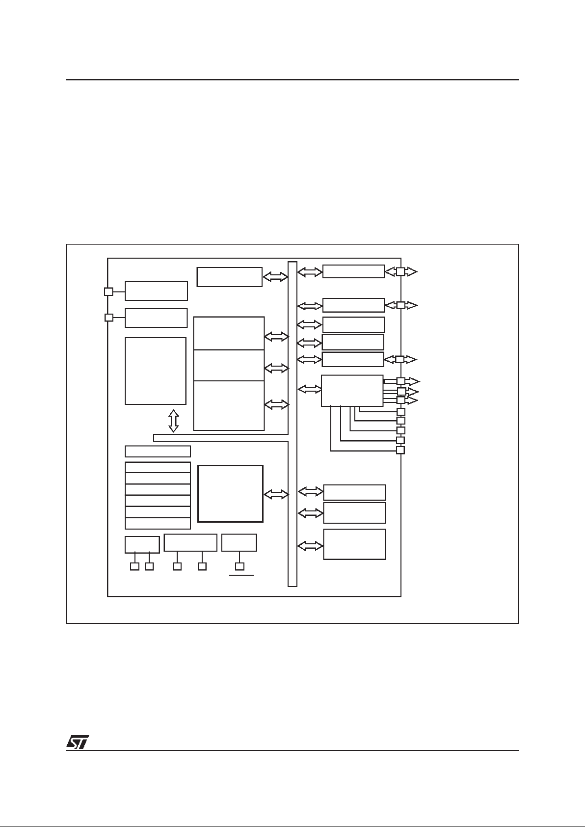
The ST62T85B and ST62E85B devices are low
cost members of the ST62xx 8-bit HCMOS family
of microcontrollers, which is targetedat low to medium complexity applications. All ST62xx devices
are based on a building block approach: a com-
mon core is surrounded by a number of on-chip
peripherals.
The ST62E85B is the erasable EPROM version of
the ST62T85B device, which may be used to emulate the ST62T85B device, as well as the respective ST6285B ROM devices.
Figure 1. Block Diagram
TEST
NMI
INTERRUPT
PROGRAM
PC
STACK LEVEL 1
STACK LEVEL 2
STACK LEVEL 3
STACK LEVEL 4
STACK LEVEL 5
STACK LEVEL 6
POWER
SUPPLY
OSCILLATOR
RESET
DATA ROM
USER
SELECTABLE
DATA RAM
PORT A
PORT B
ARTIMER
DIGITAL
8 BIT CORE
TEST/V
PP
8-BIT
A/D CONVERTER
PA5 / Scl / 20mA Sink
V
DDVSS
OSCin OSCout RESET
WATCHDOG
Memory
PORT C
SPI (SERIAL
PERIPHERAL
INTERFACE)
192 Bytes
7948 bytes
DATA EEPROM
128 Bytes
PB0 / RXD / Ain
S9..S24, S33..S56
COM9..COM16 / S1..S8
(V
PP
on EPROM/OTP versions only)
VLCD
VLCD1/5
VLCD2/5
TIMER
LCD DRIVER
VA0479
VLCD4/5
VLCD3/5
PC4..PC7/ Ain
PA6 / Sin / 20mA Sink
PA7 / Sout / 20mA Sink
PA4 / TIMER / 20mA Sink
PB2..PB3 / Ain
PB1 / TXD / Ain
COM1..COM8
UART
5

6/76
ST62T85B/E85B
INTRODUCTION (Cont’d)
OTP and EPROM devices are functionally identical. The ROM based versions offer the same functionality selecting as ROM options the options defined in the programmable option byte of the
OTP/EPROM versions.OTP devices offer all the
advantages of user programmability at low cost,
which make them the ideal choice in a wide range
of applications where frequent code changes, multiple code versions or last minute programmability
are required.
These compact low-cost devices feature one Timer comprising an 8-bit counter and a 7-bit programmable prescaler, one 8-bit autoreload timer
with 7-bit programmable prescaler (ARTimer),
EEPROM data capability, a serial synchronous
port interface (SPI), an 8-bit A/D Converter with 8
analog inputs, a Digital Watchdog timer, and a
complete LCD controller driver, making them well
suited for a wide range of automotive, appliance
and industrial applications.
6
7/76
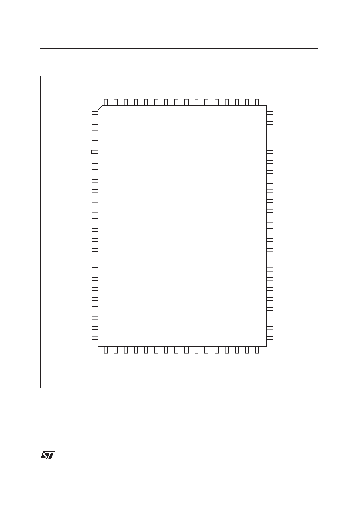
ST62T85B/E85B
Figure 2. ST6285B Pin Description
*Note: 20mA Sink
S16
S15
S14
S13
S12
S11
S10
S9
COM16/S8
COM15/S7
COM14/S6
COM13/S5
COM12/S4
COM11/S3
COM10/S2
COM9/S1
COM8
COM7
COM6
COM5
COM4
COM3
COM2
COM1
S41
S42
S43
S44
S45
S46
S47
S48
S49
S50
S51
S52
S53
S54
S55
S56
PB3
PB2
PB1
PB0
TEST/V
PP
OSCout
OSCin
RESET
1
2
3
4
5
6
7
8
9
10
11
12
13
14
15
16
17
18
19
20
21
22
23
24
64
63
62
61
60
59
58
57
56
55
54
53
52
51
50
49
48
47
46
45
44
43
42
41
80 79 78 77 76 75 74 73 72 71 70 69 68 67 66 65
25 26 27 28 29 30 31 32 37 38 39
40
S40
S39
S38
S37
S36
S35
S34
S33
S24
S23
S22
S21
S20
S19
S18
S17
PC7
PC6
PC5
PC4
NMI
V
DD
V
SS
VLCD
VLCD4/5
VLCD3/5
VLCD2/5
VLCD1/5
PA7/Sout*
PA6/Sin*
PA5/SCL*
PA4/TIM1*
33 34 35 36
7

8/76
ST62T85B/E85B
1.2 PIN DESCRIPTIONS
VDDand VSS. Power is supplied to the MCU via
these two pins. VDDis the power connection and
VSSis the ground connection.
OSCin and OSCout. These pins are internally
connected tothe on-chip oscillator circuit. A quartz
crystal, a ceramic resonator or an external clock
signal can be connected between these two pins.
The OSCin pin is the input pin, the OSCout pin is
the output pin.
RESET. The active-low RESET pin is used to restart the microcontroller.
TEST/VPP. The TEST must be held at VSSfor nor-
mal operation. If TEST pin is connected to a
+12.5V level during the reset phase, the
EPROM/OTP programming Mode is entered.
NMI. TheNMI pin provides the capability for asynchronous interruption, byapplying an external non
maskable interrupt to the MCU. The NMI input is
falling edge sensitive with Schmitt trigger characteristics. The user can select as option the availability of an on-chip pull-up at this pin.
PA4-PA7. These 4 lines are organised as one I/O
port (A). Each line may be configured under software controlas inputs with or without internal pullup resistors, interrupt generating inputs with pullup resistors, open-drain or push-pull outputs.
PA5/SCL, PA6/Sin and PA7/Sout can be used respectively as data clock, data in and clock pins for
the on-chip SPI, while PA4/TIMER can be used as
Timer I/O. In addition, PA4-PA7 can sink20mA for
direct LED or TRIAC drive.
PB0...PB3. These 4lines areorganised as one I/O
port (B). Each line may be configured under software control as inputs with or without internal pullup resistors, interrupt generating inputs with pullup resistors, open-drain or push-pull outputs, analog inputs for the A/D converter. PB0 (resp. PB1)
can also be usedas reception (resp. transmission)
line for the embedded UART.
PC4-PC7. These 4 lines are organised as one I/O
port (C). Each line may be configured under software control as input with or without internal pullup resistor, interrupt generating input with pull-up
resistor, open-drain or push-pull output, or analog
imputs for the A/D Converter.
COM1-COM8. These eight pins are the LCD peripheral common outputs. They are the outputs of
the on-chip backplane voltage generator which is
used for multiplexing the LCD lines.
COM9/S1-COM16/S8. These pins are the 8 multiplexed common/segment lines. Under software
selected control, they can act as LCD common
outputs allowing a 40x 16 dot matrix operation, or
they can act as segment outputs alowwing 48 x 8
dot matrix operation.
S9-S24, S33..S56. These pins are the 40 LCD peripheral segment outputs.
VLCD1/5, VLCD5/5. Display supplyvoltage inputs
for determining the display voltage levels on
common and segment pins during multiplex operation.
8
9/76
ST62T85B/E85B
1.3 MEMORY MAP
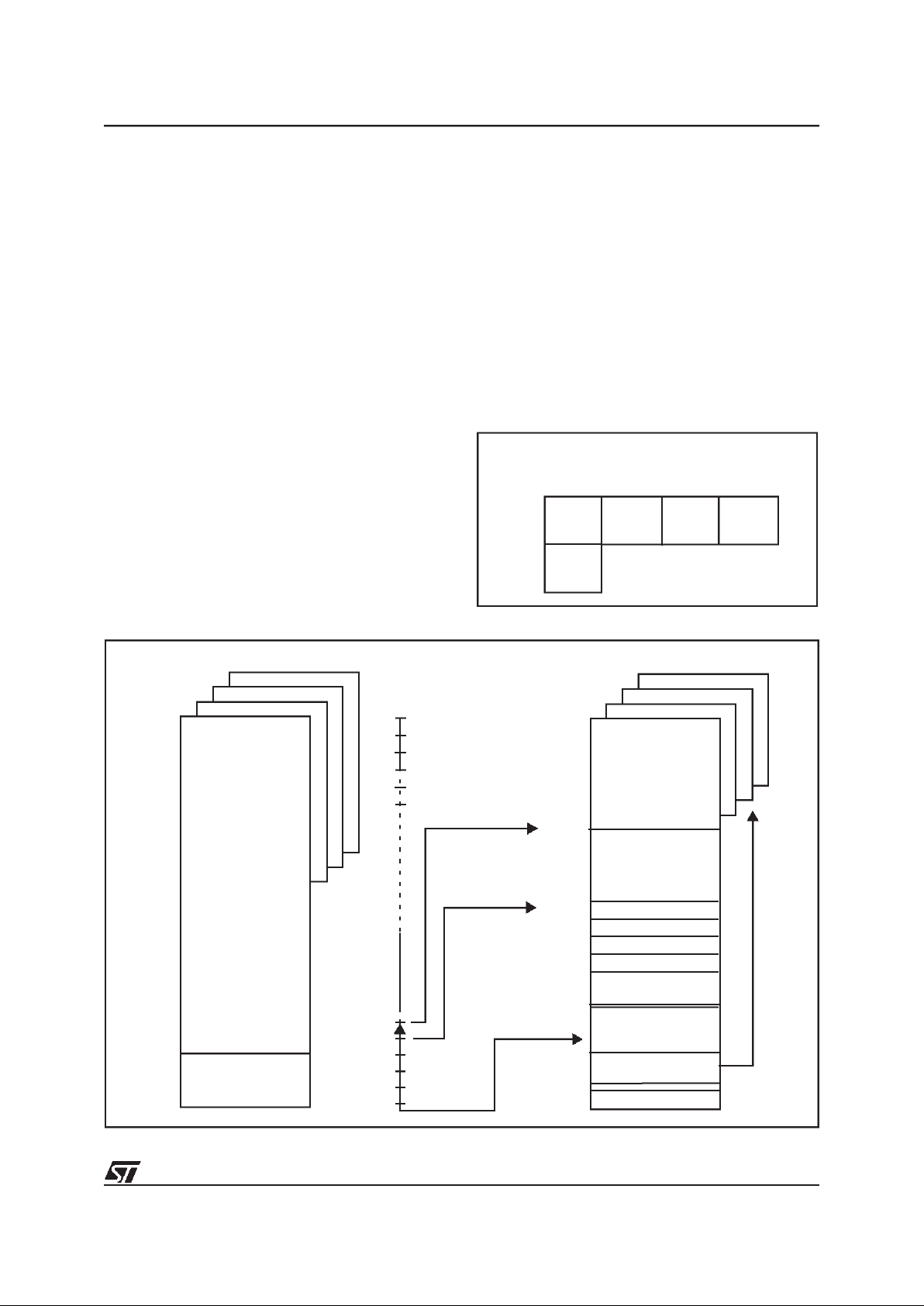
1.3.1 Introduction
The MCU operates in three separate memory
spaces: Program space, Data space, and Stack
space. Operationin these three memory spaces is
described in the following paragraphs.
Briefly, Program space contains user program
code in Program memory and user vectors; Data
space contains user data in RAM and in Program
memory, and Stack space accommodates six levels of stack for subroutine and interrupt service
routine nesting.
1.3.2 Program Space
Program Space comprises the instructions to be
executed, the data required for immediate addressing mode instructions, the reserved factory
test area and the user vectors. Program Space is
addressed via the 12-bit Program Counter register
(PC register).
Program Space is organised in four 2K pages.
Three of them are addressedin the 000h-7FFh locations of the Program Space by the Program
Counter and by writing the appropriate code in the
Program ROM Page Register (PRPR register). A
common (STATIC) 2K page is available all the
time for interrupt vectors and common subroutines, independently of the PRPR register content.
This “STATIC” page is directly addressed in the
0800h-0FFFh by the MSB of the ProgramCounter
register PC 11. Note this page can also be addressed in the 000-7FFh range. It is two different
ways of addressing the same physical memory.
Jump from a dynamic page to another dynamic
page is achieved by jumping back to the static
page, changing contents of PRPR and then jumping to the new dynamic page.
Figure 3. 8Kbytes Program Space Addressing
Figure 4. Memory Addressing Diagram
PC
SPACE
000h
7FFh
800h
FFFh
0000h
1FFFh
Page 0
Page 1
Static
Page
Page 2 Page 3
Page 1
Static
Page
ROM SPACE
PROGRAM SPACE
PROGRAM
INTERRUPT &
RESET VECTORS
ACCUMULATOR
DATA RAM
BANK SELECT
WINDOW SELECT
RAM
X REGISTER
Y REGISTER
V REGISTER
W REGISTER
DATA READ-ONLY
WINDOW
RAM / EEPROM
BANKING AREA
000h
03Fh
040h
07Fh
080h
081h
082h
083h
084h
0C0h
0FFh
0-63
DATA SPACE
0000h
0FF0h
0FFFh
MEMORY
MEMORY
DATA READ-ONLY
MEMORY
VR01568
9

10/76
ST62T85B/E85B
MEMORY MAP (Cont’d)
Table 1. ST62E85B/T80B Program MemoryMap
Note: OTP/EPROM devices can be programmed
with thedevelopment toolsavailable fromSTMicroelectronics (ST62E8X-EPB).
1.3.2.1 Program ROM Page Register (PRPR)
The PRPR register can be addressed like a RAM
location in the Data Space at the address CAh ;
nevertheless it is a write only register that cannot
be accessed with single-bit operations. This register is used to select the 2-Kbyte ROM bank of the
Program Space that will be addressed. The
number of the page has to be loaded in the PRPR
register. Refer to the Program Space description
for additional information concerning the use of
this register. The PRPR register is not modified
when an interrupt or a subroutine occurs.
Care is required when handling the PRPR register
as it is write only. For this reason, it is not allowed
to change the PRPR contents while executing interrupt service routine, as the service routine
cannot save and then restore its previous content.
This operation may be necessary if common routines and interrupt service routines take more than
2K bytes ; in this case it could be necessary to divide the interruptservice routineinto a (minor) part
in the static page (start and end) and to a second
(major) part in one ofthe dynamic pages. If it is impossible to avoid the writing ofthis register in interrupt service routines, an image of this register
must be saved in a RAM location, and each time
the program writes to the PRPR it must write also
to the image register. The image register must be
written before PRPR, so if an interrpt occurs between the two instructions the PRPR is not affected.
Program ROM Page Register (PRPR)
Address: CAh — Write Only
Bits 2-7= Not used.
Bit 5-0 = PRPR1-PRPR0:
Program ROM Select.
These two bits select the corresponding page to
be addressed in the lower part of the 4K program
address space as specified in Table 2.
This register is undefined on Reset. Neither read
nor single bit instructions may be used to address
this register.
Table 2. 8Kbytes Program ROM Page Register
Coding
1.3.2.2 Program Memory Protection
The Program Memory in OTP or EPROM devices
can be protected againstexternal readoutof memory by selecting the READOUT PROTECTION option in the option byte.
In the EPROM parts, READOUT PROTECTION
option can be disactivated only by U.V. erasure
that also results into the whole EPROM context
erasure.
Note: Once the Readout Protection is activated, it
is no longer possible, even for STMicroelectronics,
to gain access to the Program memory contents.
Returned parts with a protection set can therefore
not be accepted.
ROM Page Device Address Description
Page 0
0000h-007Fh
0080h-07FFh
Reserved
User ROM
Page 1
“STATIC”
0800h-0F9Fh
0FA0h-0FEFh
0FF0h-0FF7h
0FF8h-0FFBh
0FFCh-0FFDh
0FFEh-0FFFh
User ROM
Reserved
Interrupt Vectors
Reserved
NMI Vector
Reset Vector
Page 2
0000h-000Fh
0010h-07FFh
Reserved
User ROM
Page 3
0000h-000Fh
0010h-07FFh
Reserved
User ROM
70
- - - - - - PRPR1 PRPR0
PRPR1 PRPR0 PC bit 11 Memory Page
X X 1 Static Page (Page 1)
0 0 0 Page 0
0 1 0 Page 1 (Static Page
1 0 0 Page 2
1 1 0 Page 3
10

11/76
ST62T85B/E85B
MEMORY MAP (Cont’d)
1.3.3 Data Space
Data Space accommodates all the data necessary
for processing the user program. This space comprises the RAM resource, the processor core and
peripheral registers, as well as read-only data
such as constants and look-up tables in Program
memory.
1.3.3.1 Data ROM
All read-only data is physically stored in program
memory, which also accommodates the Program
Space. The program memory consequently contains the program code to be executed, as well as
the constants and look-up tables required by the
application.
The Data Space locations in which the different
constants and look-up tables are addressedby the
processor core may be thought of as a 64-byte
window through which it is possible to access the
read-only data stored in Program memory.
1.3.3.2 Data RAM/EEPROM
In ST62T85B and ST62E85B devices, the data
space includes 60 bytes of RAM, the accumulator
(A), the indirect registers (X), (Y), the short direct
registers (V), (W), the I/O port registers, the peripheral data and control registers, the interrupt
option register and the Data ROM Window register
(DRW register).
Additional RAM and EEPROM pages can also be
addressed using banks of 64 bytes located between addresses 00h and 3Fh.
1.3.4 Stack Space
Stack space consists of six 12-bit registers which
are used to stack subroutine and interrupt return
addresses, as well as the current program counter
contents.
Table 3. Additional RAM/EEPROM Banks.
Table 4. ST62T85B/E85B Data Memory Space
Device RAM EEPROM LCD RAM
ST62T85B/E85B 2 x 64 bytes 2 x 64 bytes 2 x 64 bytes
DATA RAM/EEPROM, LCD RAM
000h
03Fh
DATA ROM WINDOW AREA
040h
07Fh
X REGISTER 080h
Y REGISTER 081h
V REGISTER 082h
W REGISTER 083h
DATARAM
084h
0BFh
PORT A DATAREGISTER 0C0h
PORT B DATAREGISTER 0C1h
SPI INTERRUPT DISABLE REGISTER 0C2h
PORT C DATAREGISTER 0C3h
PORT A DIRECTION REGISTER 0C4h
PORT B DIRECTION REGISTER 0C5h
PORT C DIRECTION REGISTER 0C6h
RESERVED 0C7h
INTERRUPTOPTION REGISTER 0C8h*
DATAROM WINDOW REGISTER 0C9h*
ROM BANK SELECTREGISTER 0CAh*
DATARAM/EEPROM, LCD BANK SELECT REGISTER 0CBh*
PORT A OPTION REGISTE R 0CCh
RESERVED 0CDh
PORT B OPTION REGISTE R 0CEh
PORT C OPTION REGISTER 0CFh
A/D DATAREGISTER 0D0h
A/D CONTROL REGISTER 0D1h
TIMER 1 PRESCALER REGISTER 0D2h
TIMER 1 COUNTERREGISTER 0D3h
TIMER 1 STATUS/CONTROLREGISTER 0D4h
RESERVED 0D5h
UARTDATA REGISTER 0D6h
UARTCONTROL REGISTER 0D7h
WATCHDOGREGISTER 0D8h
RESERVED
0D9h
0DAh
0DBh
LCD MODE CONTROL REGISTE R 0DCh
SPI DATAREGISTER 0DDh
RESERVED 0DEh
EEPROM CONTROL REGISTER 0DFh
RESERVED
0E0h
0E4h
ARTIMER MODE/CONTROL REGISTER 0E5h
ARTIMER STATUS/CONTROL REGISTER 0 0E6h
ARTIMER STATUS/CONTROL REGISTER 1 0E7h
RESERVED
ARTIMER RELOAD/CAPTUREREGISTER 0E9h
ARTIMER COMPARE REGISTER 0EAh
ARTIMER LOAD REGISTER 0EBh
RESERVED
0ECh
0FEh
ACCUMULATOR OFFh
* WRITE ONLYREGISTER
11
12/76
ST62T85B/E85B
MEMORY MAP (Cont’d)
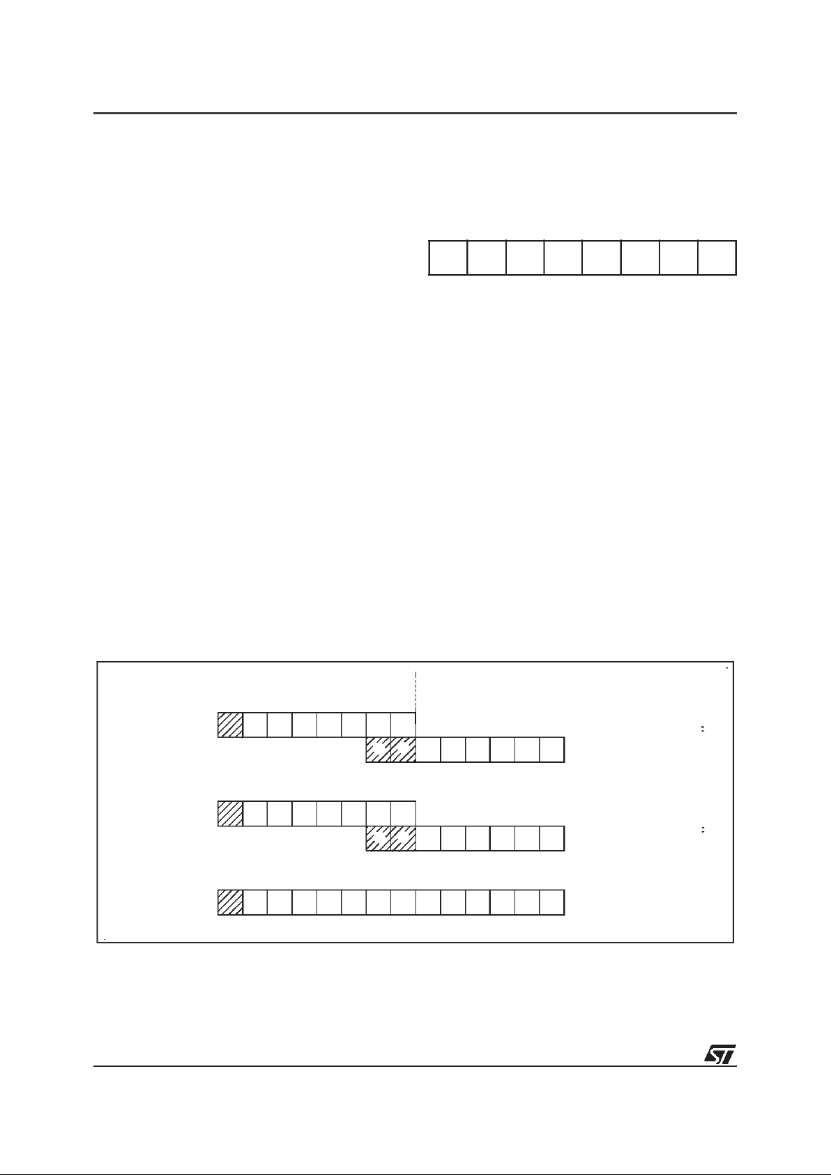
1.3.5 Data Window Register (DWR)
TheData read-only memorywindowislocatedfrom
address 0040h to address 007Fh in Data space. It
allows directreading of 64 consecutive bytes located anywhere in program memory, between address 0000h and 1FFFh (top memory address depends on the specific device). All the program
memory can therefore be used to store either instructions or read-only data. Indeed, the window
can be moved in steps of 64 bytes along the program memoryby writingtheappropriate code inthe
Data Window Register (DWR).
The DWR can beaddressed like anyRAM location
in the Data Space, it is however a write-only register and therefore cannotbe accessed using singlebit operations. This register is used to position the
64-byte read-only data window (from address 40h
to address 7Fh of the Data space) in program
memory in 64-byte steps. The effective address of
the byte to be read as data in program memory is
obtained by concatenating the 6 least significant
bits of the register address given in the instruction
(as least significant bits) and the content of the
DWR register(as most significant bits), as illustrated in Figure 5 below. For instance, when addressing location 0040h of the Data Space, with 0 loaded in the DWR register, the physical location addressed inprogram memory is 00h. The DWRregister is not cleared on reset, therefore it must be
written to prior tothe first access to the Data readonly memory window area.
Data Window Register (DWR)
Address: 0C9h — Write Only
Bits 7 = Not used.
Bit 6-0 = DWR6-DWR0:
Data read-only memory
Window Register Bits.
These are the Data readonly memory Window bits that correspond to the
upper bits of the data read-only memory space.
Caution:
This register is undefined on reset. Neither read nor single bit instructions may be used to
address this register.
Note: Care is required when handling the DWR
register as it is write only. For this reason, the
DWR contents should not be changed while executing an interrupt service routine, as the service
routine cannot saveand then restore the register’s
previous contents. If it is impossible to avoid writing to the DWR during the interrupt service routine,
an image of the register must be saved in a RAM
location, and each time the program writes to the
DWR, it must also write to the image register. The
image register must be written first so that, if an interrupt occurs between the two instructions, the
DWR is not affected.
Figure 5. Data read-only memory Window Memory Addressing
70
- DWR6 DWR5 DWR4 DWR3 DWR2 DWR1 DWR0
DATA ROM
WINDOW REGISTER
CONTENTS
DATA SPACE ADDRESS
40h-7Fh
IN INSTRUCTION
PROGRAM SPACE ADDRESS
765432 0
543210
543210
READ
1
67891011
01
VR0A1573
12
1
0
DATA SPACE ADDRESS
59h
0000
01001
11
Example:
(DWR)
DWR=28h
11
00000000
1
ROM
ADDRESS:A19h
11
13
0
1
12

13/76
ST62T85B/E85B
MEMORY MAP (Cont’d)
1.3.6 Data RAM/EEPROM and LCD RAM Bank
Register (DRBR)
Address: CBh — Write only
Bit 7 = This bit is not used
Bit 6 - DRBR6. This bit, when set, selects LCD
RAM Page 2.
Bit 5 - DRBR5. This bit, when set, selects LCD
RAM Page 1.
Bit 4 - DRBR4. This bit, when set, selects RAM
Page 2.
Bit 3 - DRBR3. This bit, when set, selects RAM
Page 1.
Bit2. These bits are not used.
Bit 1 - DRBR1. This bit, when set, selects
EEPROM Page 1.
Bit 0 - DRBR0. This bit, when set, selects
EEPROM Page 0.
The selection of the bank is made by programming
the Data RAM Bank Switch register (DRBR register) located at address CBh of the Data Space according to Table 1. No more than one bank should
be set at a time.
The DRBR register can be addressed like a RAM
Data Space at the address CBh; nevertheless it is
a write only register that cannot be accessed with
single-bit operations. This register isused to select
the desired 64-byte RAM/EEPROM bank of the
Data Space. Thenumber of banks has to be loaded in the DRBR register and the instruction has to
point to the selected location as if it was in bank 0
(from 00h address to 3Fh address).
This register is not cleared during the MCU initialization, therefore it must be written before the first
access to the Data Space bank region. Refer to
the Data Space description for additional information. The DRBR register is not modified when an
interrupt or a subroutine occurs.
Notes :
Care is required when handling the DRBR register
as it is write only. For this reason, it is not allowed
to change the DRBR contents while executing interrupt service routine, as the service routine cannot save and thenrestore its previous content. If it
is impossible to avoid the writing of this register in
interrupt service routine, an image of this register
must be saved in a RAM location, and each time
the program writes to DRBR it must write also to
the image register. The image register must be
written first, so if an interrupt occurs between the
two instructions the DRBR is not affected.
In DRBR Register, only 1 bit must be set. Otherwise two or more pages are enabled in parallel,
producing errors.
Table 5. Data RAM Bank Register Set-up
70
- DRBR6 DRBR5 DRBR4 DRBR3 - DRBR1 DRBR0
DRBR ST62T85B/E85B
00 None
01 EEPROM Page 0
02 EEPROM Page 1
08 RAM Page 1
10h RAM Page 2
20h LCD RAM Page 1
40h LCD RAM Page 2
other Reserved
13
14/76
ST62T85B/E85B
MEMORY MAP (Cont’d)
1.3.7 EEPROM Description
EEPROM memory is located in 64-byte pages in
data space. This memory maybe used by theuser
program for non-volatile data storage.
Data spacefrom 00h to3Fh is paged as described
in Table 6. EEPROM locations are accessed directly by addressing these paged sections of data
space.
The EEPROM does not require dedicated instructions forreadorwrite access.Onceselectedvia the
Data RAM Bank Register, the active EEPROM
page is controlled by the EEPROM Control Register (EECTL), which is described below.
Bit E20FFof the EECTL registermust bereset prior
to any write or read access to the EEPROM. If no
bank hasbeen selected, or if E2OFF is set, any access is meaningless.
Programming must be enabled by setting the
E2ENA bit of the EECTL register.
The E2BUSY bitof the EECTL register is setwhen
the EEPROM is performing a programming cycle.
Any access to the EEPROM when E2BUSY is set
is meaningless.
Provided E2OFF and E2BUSY are reset, an EEPROM location is read just like any other data location, also in terms of access time.
Writing to the EEPROM may be carried out in two
modes: Byte Mode (BMODE) and Parallel Mode
(PMODE). In BMODE, one byte is accessed at a
time, while in PMODE up to 8 bytes in the same
row are programmed simultaneously (with consequent speed and power consumption advantages,
the latter being particularly important in battery
powered circuits).
General Notes:
Data should be written directly to the intended ad-
dress in EEPROM space. There is nobuffer memory between data RAM and the EEPROM space.
When the EEPROM is busy (E2BUSY = “1”)
EECTL cannot be accessed in write mode, it is
only possible to read the status of E2BUSY. This
implies that as long as the EEPROM is busy, it is
not possible to change the status of the EEPROM
Control Register. EECTL bits 4 and 5 are reserved
and must never be set.
Care is required whendealing withthe EECTL register, as some bits are write only. For this reason,
the EECTL contents must not be altered while executing an interrupt service routine.
If it is impossible to avoid writing to this register
within an interrupt service routine, an image of the
register must be saved in a RAM location, and
each time the program writes to EECTL it must
also write to the image register.The image register
must be written to first so that, if an interrupt occurs between the two instructions, the EECTL will
not be affected.
Table 6. Row Arrangement for Parallel Writing of EEPROM Locations
Dataspace
addresses.
Banks 0 and 1.
Byte 0 1234567
ROW7 38h-3Fh
ROW6 30h-37h
ROW5 28h-2Fh
ROW4 20h-27h
ROW3 18h-1Fh
ROW2 10h-17h
ROW1 08h-0Fh
ROW0 00h-07h
Up to 8 bytes in each row may be programmed simultaneously in Parallel Write mode.
The number of available 64-byte banks (1 or 2) is device dependent.
14

15/76
ST62T85B/E85B
MEMORY MAP (Cont’d)
Additional Notes on Parallel Mode:
If the user wishes to perform parallel programming, the first step should be to set the E2PAR2
bit. From this time on, the EEPROM will be addressed in write mode, the ROW address will be
latched and it will be possible to change it only at
the end of the programming cycle, or by resetting
E2PAR2 without programming the EEPROM. After the ROW addressis latched,the MCU can only
“see” the selected EEPROM row and any attempt
to write or read other rows will produce errors.
The EEPROM should not be read while E2PAR2
is set.
As soon as the E2PAR2 bit is set, the 8 volatile
ROW latches are cleared. From this moment on,
the user can load data in allor in part ofthe ROW.
Setting E2PAR1 will modify the EEPROM registers corresponding to the ROW latches accessed
after E2PAR2. For example, if the software sets
E2PAR2 and accesses the EEPROM by writing to
addresses 18h, 1Ah and 1Bh, and then sets
E2PAR1, these three registers will be modified simultaneously; the remaining bytes in the row will
be unaffected.
Note that E2PAR2 is internally reset at the end of
the programming cycle. This implies that the user
must setthe E2PAR2 bit between two parallel programming cycles. Note that if the user tries to set
E2PAR1 while E2PAR2 is not set, there will be no
programming cycleand the E2PAR1 bit will be unaffected. Consequently, the E2PAR1bit cannot be
set if E2ENA is low. The E2PAR1 bit can be setby
the user, only if the E2ENA and E2PAR2 bits are
also set.
EEPROM Control Register (EECTL)
Address: DFh — Read/Write
Reset status: 00h
Bit 7 = D7:
Unused.
Bit6= E2OFF:
Stand-byEnable Bit.
WRITE ONLY.
IfthisbitissettheEEPROMisdisabled(anyaccess
will bemeaningless) and the power consumption of
the EEPROM is reduced to its lowest value.
Bit 5-4 = D5-D4:
Reserved.
MUST be kept reset.
Bit 3 = E2PAR1:
Parallel Start Bit.
WRITE ONLY.
OnceinParallelMode,as soonastheuser software
sets the E2PAR1 bit, parallel writing of the 8 adjacent registers will start. This bit is internally reset at
the end of the programming procedure. Note that
less than 8 bytescan bewritten if required, the undefined bytes being unaffected by the parallel programmingcycle;thisis explained ingreater detailin
the Additional Notes on Parallel Mode overleaf.
Bit 2 = E2PAR2:
Parallel Mode En. Bit.
WRITE
ONLY. This bit must be set by the user program in
order to perform parallel programming. If E2PAR2
is set and the parallel start bit (E2PAR1) is reset,
up to 8 adjacent bytes can be written simultaneously. These 8 adjacent bytes are considered as a
row, whose address lines A7, A6, A5, A4, A3 are
fixed while A2, A1 and A0 are the changingbits, as
illustrated in Table 6. E2PAR2 is automatically reset at the end of any parallel programming procedure. It can be reset by the user software before
starting the programming procedure, thus leaving
the EEPROM registers unchanged.
Bit 1 = E2BUSY:
EEPROM Busy Bit.
READ ONLY. This bit is automatically set by the EEPROM
control logic when the EEPROM is in programming mode. The userprogram should test it before
any EEPROM read or write operation; any attempt
to access the EEPROM while the busy bit is set
will be aborted and the writing procedure in
progress will be completed.
Bit 0 = E2ENA:
EEPROM Enable Bit.
WRITE ONLY. This bit enables programming of the EEPROM
cells. It must be set before any write to the EEPROM register. Any attempt to write to the EEPROM when E2ENA is low is meaningless and will
not trigger a write cycle.
70
D7 E2OFF D5 D4 E2PAR1 E2PAR2 E2BUSY E2ENA
15

16/76
ST62T85B/E85B
1.4 PROGRAMMING MODES
1.4.1 Option Byte
The Option Byte allows configuration capability to
the MCUs. Option byte’s content is automatically
read, and the selected options enabled, when the
chip reset is activated.
It can only be accessed during the programming
mode. This access is made either automatically
(copy from a master device) or by selecting the
OPTION BYTE PROGRAMMING modeof the programmer.
The option byte is located in a non-user map. No
address has to be specified.
EPROM Code Option Byte
Bit 7-6. Reserved.
Bit 5= PROTECT. This bit allows the protection of
the software contents against piracy. When the bit
PROTECT is set high, readout of the OTP contents is prevented by hardware. No programming
equipment is able to gain access to the user program. When this bit is low, the user program can
be read.
Bit 4. Reserved.
Bit 3 = NMI PULL. . This bit must beset highto en-
able the internal pull-up resistor. When low, no
pull-up is provided.
Bit 2. Reserved.
Bit 1 = WDACT. This bit controls the watchdog ac-
tivation. When it is high, hardware activation is selected. The software activation is selected when
WDACT is low.
Bit 0 = Reserved.
The Option byte is written during programming ei-
ther by using the PC menu (PC driven Mode) or
automatically (stand-alone mode)
1.4.2 Program Memory
EPROM/OTP programming mode is set by a
+12.5V voltage applied to the TEST/VPPpin. The
programming flow of the ST62T85B/E85B is described in the User Manual of the EPROM Programming Board.
The MCUs can be programmed with the
ST62E8xB EPROM programming tools available
from STMicroelectronics.
1.4.3 EEPROM Data Memory
EEPROM data pages are supplied in the virgin
state FFh. Partial or total programming of EEPROM data memory can be performed either
through the application software, or through anexternal programmer. Any STMicroelectronics tool
used for the program memory (OTP/EPROM) can
also be used to program the EEPROM data memory.
1.4.4 EPROM Erasing
The EPROM of the windowed package of the
MCUs may be erased by exposure to Ultra Violet
light. The erasure characteristic of the MCUs is
such that erasure begins when the memory is exposed to light with a wave lengths shorter than approximately 4000Å. It should be noted that sunlights and some types of fluorescent lamps have
wavelengths in the range 3000-4000Å.
It is thus recommended that the window of the
MCUs packages be covered by an opaque label to
prevent unintentional erasure problems when testing the application in such an environment.
The recommended erasure procedure of the
MCUs EPROM is the exposure to short wave ultraviolet light which have a wave-length 2537A.
The integrated dose (i.e. U.V. intensity x exposure
time) for erasure should be a minimum of 15Wsec/cm2. The erasure time with this dosage is approximately 15 to 20 minutes using an ultraviolet
lamp with 12000µW/cm2power rating. The
ST62E85B should be placed within 2.5cm (1Inch)
of the lamp tubes during erasure.
70
--
PRO-
TECT
-
NMI
PULL
- WDACT -
16

17/76
ST62T85B/E85B
2 CENTRAL PROCESSING UNIT
2.1 INTRODUCTION
The CPU Coreof ST6devicesisindependent ofthe
I/O or Memory configuration. As such, it may be
thought of as an independent central processor
communicating with on-chip I/O, Memory and Peripherals via internal address, data, and control
buses. In-core communication is arranged as
shown in Figure 6; the controller being externally
linked to both the Reset and Oscillator circuits,
while thecore is linked to thededicated on-chip peripherals via the serial data bus and indirectly, for
interrupt purposes, through the control registers.
2.2 CPU REGISTERS
TheST6FamilyCPUcorefeaturessixregisters and
three pairs of flags available to the programmer.
These are described in the following paragraphs.
Accumulator (A). The accumulator is an 8-bit
general purpose register used in all arithmetic calculations, logical operations, and data manipulations. The accumulator can be addressed in Data
space as a RAM location at address FFh. Thus the
ST6 can manipulate the accumulator just like any
other register in Data space.
Indirect Registers (X, Y). These two indirect registers are used as pointers to memory locations in
Data space. They are used in the register-indirect
addressing mode. These registers can be addressed in the dataspace as RAM locations at addresses 80h (X) and 81h (Y). They can also beaccessed with the direct, short direct, or bit direct addressing modes. Accordingly, the ST6 instruction
set can usethe indirect registers as any other register of the data space.
Short Direct Registers (V, W). These two registers are used to save a byte in short direct addressing mode. They can be addressed in Data
space as RAM locations at addresses 82h (V)and
83h (W). They can also be accessed using the direct and bit direct addressing modes. Thus, the
ST6 instruction set can use the short direct registers as any other register of the data space.
Program Counter (PC). The program counter is a
12-bit register which contains the address of the
next ROM location to be processed by the core.
This ROM location may be an opcode, an operand, or the address of an operand. The 12-bit
length allows the direct addressing of 4096 bytes
in Program space.
Figure 6. ST6 Core Block Diagram
PROGRAM
RESET
OPCODE
FLAG
VALUES
2
CONTROLLER
FLAGS
ALU
A-DATA
B-DATA
ADDRESS/READ LINE
DATA SPACE
INTERRUPTS
DATA
RAM/EEPROM
DATA
ROM/EPROM
RESULTS TO DATA SPACE (WRITE LINE)
ROM/EPROM
DEDICATIONS
ACCUMULATOR
CONTROL
SIGNALS
OSCin
OSCout
ADDRESS
DECODER
256
12
Program Counter
and
6 LAYER STACK
0,01 TO 8MHz
VR01811
17
18/76
ST62T85B/E85B
CPU REGISTERS (Cont’d)
However, ifthe program space contains more than
4096 bytes, the additional memory in program
space can be addressed by using the Program
Bank Switch register.
The PC value is incremented after reading the address of the current instruction. Toexecute relative
jumps, the PC and the offset are shifted through
the ALU, where they are added; the result is then
shifted backinto the PC.The programcounter can
be changedin the following ways:
- JP (Jump) instructionPC=Jump address
- CALL instructionPC= Call address
- Relative Branch Instruction.PC= PC +/- offset
- Interrupt PC=Interrupt vector
- Reset PC= Reset vector
- RET & RETI instructionsPC= Pop (stack)
- Normal instructionPC=PC + 1
Flags (C, Z). The ST6 CPU includes three pairs of
flags (Carry and Zero), each pair being associated
with one of the three normal modes of operation:
Normal mode, Interrupt mode and Non Maskable
Interrupt mode. Each pair consists of a CARRY
flag and a ZERO flag. One pair (CN, ZN) is used
during Normal operation, another pair is used during Interrupt mode (CI, ZI), and a third pair is used
in the Non Maskable Interrupt mode (CNMI, ZNMI).
The ST6 CPU uses the pair of flags associated
with the current mode: as soon as an interrupt (or
a Non Maskable Interrupt) is generated, the ST6
CPU uses the Interrupt flags (resp. the NMI flags)
instead of the Normal flags. When the RETI instruction is executed, the previously used set of
flags is restored. It should be noted that each flag
set can only be addressed in its own context (Non
Maskable Interrupt, Normal Interrupt or Main routine). The flags are not cleared during context
switching and thus retain their status.
The Carry flag is set when a carry or a borrow occurs during arithmetic operations; otherwise it is
cleared. The Carry flag is also set to the value of
the bit tested in a bit test instruction; it also participates in the rotate left instruction.
The Zero flag is set if the result of the last arithmetic or logical operation was equal to zero; otherwise it is cleared.
Switching between the three sets of flags is performed automatically when an NMI, an interrupt or
a RETI instructions occurs. As the NMI mode is
automatically selected after the reset of the MCU,
the ST6 core uses at first the NMI flags.
Stack. The ST6 CPU includes a true LIFO hardware stack which eliminates the need for a stack
pointer. The stack consists of six separate 12-bit
RAM locations that do not belong to the data
space RAM area. When a subroutine call (or interrupt request) occurs, the contents of each level are
shifted intothe next higher level, while the content
of the PC is shifted into the first level (the original
contents of the sixth stack level are lost). When a
subroutine or interruptreturn occurs (RET or RETI
instructions), the first level register is shifted back
into the PC and the value of each level is popped
back into the previous level. Since the accumulator, in common with all other data space registers,
is not stored in this stack, management of these
registers should be performed within the subroutine. The stack will remain in its “deepest” position
if morethan 6 nested calls orinterrupts are executed, and consequently the last return address will
be lost. It will also remain in its highest position if
the stack is emptyand aRET or RETI is executed.
In this case the next instruction will be executed.
Figure 7. ST6 CPU Programming Mode
l
SHORT
DIRECT
ADDRESSING
MODE
VREGISTER
W REGISTER
PROGRAMCOUNTER
SIX LEVELS
STACKREGISTER
CZNORMAL FLAGS
INTERRUPTFLAGS
NMI FLAGS
INDEX
REGISTER
VA000 4 23
b7
b7
b7
b7
b7
b0
b0
b0
b0
b0
b0b11
ACCUM ULATOR
Y REG. POINTER
X REG. POINTER
CZ
CZ
18
19/76
ST62T85B/E85B
3 CLOCKS, RESET, INTERRUPTS AND POWER SAVING MODES
3.1 CLOCK SYSTEM
3.1.1 Main Oscillator
The MCU featuresa Main Oscillator which can be
driven by an external clock, or used in conjunction
with an AT-cut parallel resonant crystal or a suitable ceramic resonator.
Figure 8 illustrates various possible oscillator configurations using anexternal crystal or ceramic resonator, an external clock input. CL1an CL2should
have acapacitance in the range 12 to 22 pF for an
oscillator frequency in the 4-8 MHz range.
The internal MCU clock Frequency (F
INT
) is divided by 13 to drive the CPU core and by 12 to drive
the A/D converter and the watchdog timer, while
clock used to drive on-chip peripherals depends
on the peripheral as shown in the clock circuit
block diagram.
With an 8MHz oscillator frequency, the fastest machine cycle is therefore 1.625µs.
A machine cycle is the smallest unit of time needed
to executeany operation (for instance, toincrement
the Program Counter). An instruction may require
two, four, or five machine cycles for execution.
Figure 8. Oscillator Configurations
Figure 9. Clock Circuit Block Diagram
OSC
in
OSC
out
C
L1n
C
L2
ST6xxx
CRYSTAL/RESONATOR CLOCK
OSC
in
OSC
out
ST6xxx
EXTERNAL CLOCK
NC
VA0016
VA0015A
MAIN
OSCILLATOR
Core
:13
:12
Timer 1 & 2
Watchdog
POR
f
INT
ADC
OSCin
OSCout
f
OSC
f
INT
LCD
CONTROLLER
DRIVER
& Artimer
19

20/76
ST62T85B/E85B
3.2 RESETS
The MCU can be reset in three ways:
– by the external Reset input being pulled low;
– by Power-on Reset;
– by the digital Watchdog peripheral timing out.
3.2.1 RESET Input
The RESET pin may be connected to a device of
the application board in order to reset the MCU if
required. The RESET pin may be pulled low in
RUN, WAIT or STOP mode. This input can be
used to reset the MCU internal state and ensure a
correct start-up procedure. The pin is active low
and features a Schmitt trigger input. The internal
Reset signal is generated by adding a delay to the
external signal. Therefore even short pulses on
the RESET pin are acceptable, provided VDDhas
completed its risingphase andthat the oscillator is
running correctly (normal RUN or WAIT modes).
The MCU is kept in the Reset state as long as the
RESET pin is held low.
If RESET activation occurs in the RUN or WAIT
modes, processing of the user program is stopped
(RUN modeonly), the Inputs and Outputs are configured as inputs with pull-up resistors and the
main Oscillator is restarted. When the level on the
RESET pin then goes high, the initialization sequence is executed following expiry of the internal
delay period.
If RESET pin activation occurs in the STOP mode,
the oscillator starts up and all Inputs and Outputs
are configured as inputs with pull-up resistors.
When the level of the RESET pin then goes high,
the initialization sequence is executed following
expiry of the internal delay period.
3.2.2 Power-on Reset
The function of the POR circuit consists in waking
up the MCU at an appropriate stage during the
power-on sequence. At the beginning of this sequence, the MCU is configured in the Reset state:
all I/O ports are configured as inputs with pull-up
resistors and no instruction is executed. When the
power supplyvoltage rises to a sufficient level, the
oscillator starts to operate, whereupon an internal
delay is initiated, in order to allow the oscillator to
fully stabilize before executing the first instruction.
The initialization sequence isexecuted immediately following the internal delay.
The internaldelay isgenerated byan on-chipcounter. Theinternal reset lineis released 2048 internal
clock cycles after release of the external reset.
Notes:
To ensure correct start-up, the user should take
care that the reset signal is not released before the
VDDlevel is sufficient to allow MCU operation at
the chosen frequency (see Recommended Operating Conditions).
A proper reset signal for a slow rising VDDsupply
can generally be provided by an external RC network connected to the RESET pin.
Figure 10. Reset and Interrupt Processing
INT LATCH CLEARED
NMI MASK SET
RESET
( IF PRESENT )
SELECT
NMI MODE FLAGS
IS RESET STILL
PRESENT?
YES
PUT FFEH
ON ADDRESS BUS
FROM RESET LOCATIONS
FFE/FFF
NO
FETCH INSTRUCTION
LOAD PC
VA000427
20
21/76
ST62T85B/E85B
RESETS (Cont’d)
3.2.3 Watchdog Reset
The MCU provides a Watchdog timer function in
order to ensure graceful recovery from software
upsets. If the Watchdog register is not refreshed
before an end-of-count condition is reached, the
internal reset will be activated. This, amongst other things, resets the watchdog counter.
The MCU restarts just as though the Reset had
been generated by the RESET pin, including the
built-in stabilisation delay period.
3.2.4 Application Notes
No external resistor is required between VDDand
the Reset pin, thanks to the built-in pull-up device.
The POR circuit operates dynamically, in that it
triggers MCU initialization on detecting the rising
edge of VDD. The typical threshold is in the region
of 2 volts, but the actual value of the detected
threshold depends on the way in which VDDrises.
The POR circuit is
NOT
designed to supervise
static, or slowly rising or falling VDD.
3.2.5 MCU Initialization Sequence
When a reset occurs the stack is reset, the PC is
loaded with the address of the Reset Vector (located in program ROM starting at address 0FFEh). A
jump tothe beginning of theuser program must be
coded at this address. Following a Reset, the Interrupt flag is automatically set, so that the CPU is
in Non Maskable Interrupt mode; this prevents the
initialisation routine from being interrupted. The initialisation routine should therefore be terminated
by a RETI instruction, in order to revert to normal
mode and enable interrupts. Ifno pending interrupt
is presentat theend of the initialisation routine, the
MCU will continue by processing the instruction
immediately following the RETI instruction. If, however, a pending interrupt is present, it will be serviced.
Figure 11. Reset and Interrupt Processing
Figure 12. Reset Block Diagram
RESET
RESET
VECTOR
JP
JP:2 BYTES/4 CYCLES
RETI
RETI: 1 BYTE/2 CYCLES
INITIALIZATION
ROUTINE
VA00181
V
DD
RESET
300kΩ
2.8kΩ
POWER
WATCHDOG RESET
CK
COUNTER
RESET
ST6
INTERNAL
RESET
f
OSC
RESET
ON RESET
VA0200B
21

22/76
ST62T85B/E85B
RESETS (Cont’d)
Table 7. Register Reset Status
Register Address(es) Status Comment
EEPROM Control Register
Port Data Registers
Port A,B Direction Register
Port A,B Option Register
Interrupt Option Register
SPI Registers
LCD Mode Control Register
0DFh
0C0h, 0C1h, 0C3h
0C4h to 0C6h
0CCh, 0CEh, OCFh
0C8h
0C2h, 0DDh
0DCh
00h
EEPROM enabled
I/O are Input with pull-up
Interrupt disabled
SPI disabled
LCD display off
UART Control
UART Data Register
00h UART disabled
X, Y,V, W, Register
Accumulator
Data RAM
Data RAM/EEPROM/LCDRAM Page Register
Data ROM Window Register
EEPROM
A/D Result Register
080H TO 083H
0FFh
084h to 0BFh
0CBh
0C9h
00h to 03Fh
0D0h
Undefined As written if programmed
TIMER 1 Status/Control
TIMER 1 Counter Register
TIMER 1 Prescaler Register
Watchdog Counter Register
A/D Control Register
0D4h
0D3h
0D2h
0D8h
0D1h
00h
FFh
7Fh
FEh
40h
TIMER 1 disabled/Max count
loaded
A/D in Standby
AR TIMER Mode Control Register
AR TIMER Status/Control 1 Register
AR TIMER Status/Control 2Register
AR TIMER Compare Register
AR TIMER Load Register
AR TIMER Reload/Capture Register
0E5h
0E6h
0E7h
0EAh
0EBh
0E9h
00h
Undefined
AR TIMER stopped
As written if programmed
22

23/76
ST62T85B/E85B
3.3 DIGITAL WATCHDOG
The digital Watchdog consists of a reloadable
downcounter timer which can be used to provide
controlled recovery from software upsets.
The Watchdog circuit generates a Reset when the
downcounter reaches zero. User software can
prevent this reset by reloading the counter, and
should therefore be written so that the counter is
regularly reloaded while the user program runs
correctly. Inthe event of a software mishap (usually caused by externally generated interference),
the userprogram will no longer behave in its usual
fashion and the timer register will thus not be reloaded periodically. Consequently the timer will
decrement down to 00h and reset the MCU. In order to maximise the effectiveness of the Watchdog
function, user software must be written with this
concept in mind.
Watchdog behaviour is governed by one option,
known as “WATCHDOG ACTIVATION” (i.e.
HARDWARE or SOFTWARE) (See Table8).
In the SOFTWARE option, the Watchdog is disabled until bit C of the DWDR register has been set.
When the Watchdog is disabled, low power Stop
mode is available. Once activated, the Watchdog
cannot be disabled, except by resetting the MCU.
In the HARDWARE option, the Watchdog is permanently enabled. Sincethe oscillatorwill run continuously, low power mode is not available. The
STOP instruction is interpreted as a WAIT instruction, and the Watchdog continues to countdown.
When the MCU exits STOP mode (i.e. when aninterrupt is generated), the Watchdog resumes its
activity.
Table 8. Recommended Option Choices
Functions Required Recommended Options
Stop Mode “SOFTWARE WATCHDOG”
Watchdog “HARDWARE WATCHDOG”
23
 Loading...