

SGS Thomson Microelectronics ST62T62BM6, ST62T62BM3, ST62T52BM6, ST62T52BM3, ST62P52BM6 Datasheet
...
April 1998 1/68
R
ST62T52B
ST62T62B/E62B
8-BIT OTP/EPROM MCUs WITH
A/D CONVERTER, AUTO-RELOAD TIMER AND EEPROM
■
3.0 to 6.0V Supply Operating Range
■
8 MHz Maximum Clock Frequency
■
-40 to +125°C Operating Temperature Range
■
Run, Wait and Stop Modes
■
5 Interrupt Vectors
■
Look-up Table capability in Program Memory
■
Data Storage in Program Memory:
User selectable size
■
Data RAM: 128 bytes
■
Data EEPROM: 64 bytes (none on ST 62T 52B)
■
User Programmable Options
■
9 I/O pins, fully programmable as:
– Input with pull-up resistor
– Input without pull-up resistor
– Input with interrupt generation
– Open-drain or push-pull output
– Analog Input
■
5 I/O lines can sink up to 20mA to drive LEDs or
TRIACs directly
■
8-bit Timer/Counter with 7-bit programmable
prescaler
■
8-bit Auto-reload Timer with 7-bit programmable
prescaler (AR Timer)
■
Digital Watchdog
■
8-bit A/D Converter with 4 analog inputs
■
On-chip Clock oscillator can be driven by Quartz
Crystal Ceramic resonator or RC network
■
User configurable Power-on Reset
■
One external Non-Maskable Interrupt
■
ST626x-EMU2 Emulation and Development
System (connects to an MS-DOS PC via a
parallel port)
DEVICE SUMMARY
(See end of Datasheet for Ordering Information)
PDIP16
PSO16
CDIP16W
DEVICE
EPROM
(Bytes)
OTP
(Bytes)
EEPROM
ST62T52B 1836 ST62T62B 1836 64
ST62E62B 1836 64
1
Rev. 2.4

2/68
Table of Contents
68
2
ST62T52B / ST62T62B/E62B . . . . . . . . . . . . . . . . . . . . . . . . . . . 1
1 GENERAL DESCRIPTION . . . . . . . . . . . . . . . . . . . . . . . . . . . . . . . . . . . . . . . . . . . . . . . . . . . . . . 4
1.1 INTRODUCTION . . . . . . . . . . . . . . . . . . . . . . . . . . . . . . . . . . . . . . . . . . . . . . . . . . . . . . . . . 4
1.2 PIN DESCRIPTIONS . . . . . . . . . . . . . . . . . . . . . . . . . . . . . . . . . . . . . . . . . . . . . . . . . . . . . . 5
1.3 MEMORY MAP . . . . . . . . . . . . . . . . . . . . . . . . . . . . . . . . . . . . . . . . . . . . . . . . . . . . . . . . . . 6
1.3.1 Introduction . . . . . . . . . . . . . . . . . . . . . . . . . . . . . . . . . . . . . . . . . . . . . . . . . . . . . . . . 6
1.3.2 Program Space . . . . . . . . . . . . . . . . . . . . . . . . . . . . . . . . . . . . . . . . . . . . . . . . . . . . . 7
1.3.3 Data Space . . . . . . . . . . . . . . . . . . . . . . . . . . . . . . . . . . . . . . . . . . . . . . . . . . . . . . . . 8
1.3.4 Stack Space . . . . . . . . . . . . . . . . . . . . . . . . . . . . . . . . . . . . . . . . . . . . . . . . . . . . . . . . 8
1.3.5 Data Window Register (DWR) . . . . . . . . . . . . . . . . . . . . . . . . . . . . . . . . . . . . . . . . . . 9
1.3.6 Data RAM/EEPROM Bank Register (DRBR) . . . . . . . . . . . . . . . . . . . . . . . . . . . . . . 10
1.3.7 EEPROM Description . . . . . . . . . . . . . . . . . . . . . . . . . . . . . . . . . . . . . . . . . . . . . . . 11
1.4 PROGRAMMING MODES . . . . . . . . . . . . . . . . . . . . . . . . . . . . . . . . . . . . . . . . . . . . . . . . . 13
1.4.1 Option Byte . . . . . . . . . . . . . . . . . . . . . . . . . . . . . . . . . . . . . . . . . . . . . . . . . . . . . . . 13
1.4.2 Program Memory . . . . . . . . . . . . . . . . . . . . . . . . . . . . . . . . . . . . . . . . . . . . . . . . . . . 13
1.4.3 . EEPROM Data Memory . . . . . . . . . . . . . . . . . . . . . . . . . . . . . . . . . . . . . . . . . . . . . 13
2 CENTRAL PROCESSING UNIT . . . . . . . . . . . . . . . . . . . . . . . . . . . . . . . . . . . . . . . . . . . . . . . . . 14
2.1 INTRODUCTION . . . . . . . . . . . . . . . . . . . . . . . . . . . . . . . . . . . . . . . . . . . . . . . . . . . . . . . . 14
2.2 CPU REGISTERS . . . . . . . . . . . . . . . . . . . . . . . . . . . . . . . . . . . . . . . . . . . . . . . . . . . . . . . 14
3 CLOCKS, RESET, INTERRUPTS AND POWER SAVING MODES . . . . . . . . . . . . . . . . . . . . . 16
3.1 CLOCK SYSTEM . . . . . . . . . . . . . . . . . . . . . . . . . . . . . . . . . . . . . . . . . . . . . . . . . . . . . . . . 16
3.1.1 Main Oscillator . . . . . . . . . . . . . . . . . . . . . . . . . . . . . . . . . . . . . . . . . . . . . . . . . . . . . 16
3.2 RESETS . . . . . . . . . . . . . . . . . . . . . . . . . . . . . . . . . . . . . . . . . . . . . . . . . . . . . . . . . . . . . . . 18
3.2.1 RESET Input . . . . . . . . . . . . . . . . . . . . . . . . . . . . . . . . . . . . . . . . . . . . . . . . . . . . . . 18
3.2.2 Power-on Reset . . . . . . . . . . . . . . . . . . . . . . . . . . . . . . . . . . . . . . . . . . . . . . . . . . . . 18
3.2.3 Watchdog Reset . . . . . . . . . . . . . . . . . . . . . . . . . . . . . . . . . . . . . . . . . . . . . . . . . . . 19
3.2.4 Application Notes . . . . . . . . . . . . . . . . . . . . . . . . . . . . . . . . . . . . . . . . . . . . . . . . . . . 19
3.2.5 MCU Initialization Sequence . . . . . . . . . . . . . . . . . . . . . . . . . . . . . . . . . . . . . . . . . . 19
3.3 DIGITAL WATCHDOG . . . . . . . . . . . . . . . . . . . . . . . . . . . . . . . . . . . . . . . . . . . . . . . . . . . . 21
3.3.1 Digital Watchdog Register (DWDR) . . . . . . . . . . . . . . . . . . . . . . . . . . . . . . . . . . . . . 23
3.3.2 Application Notes . . . . . . . . . . . . . . . . . . . . . . . . . . . . . . . . . . . . . . . . . . . . . . . . . . . 23
3.4 INTERRUPTS . . . . . . . . . . . . . . . . . . . . . . . . . . . . . . . . . . . . . . . . . . . . . . . . . . . . . . . . . . 25
3.4.1 Interrupt request . . . . . . . . . . . . . . . . . . . . . . . . . . . . . . . . . . . . . . . . . . . . . . . . . . . . 25
3.4.2 Interrupt Procedure . . . . . . . . . . . . . . . . . . . . . . . . . . . . . . . . . . . . . . . . . . . . . . . . . 26
3.4.3 Interrupt Option Register (IOR) . . . . . . . . . . . . . . . . . . . . . . . . . . . . . . . . . . . . . . . . 27
3.4.4 Interrupt Sources . . . . . . . . . . . . . . . . . . . . . . . . . . . . . . . . . . . . . . . . . . . . . . . . . . . 27
3.5 POWER SAVING MODES . . . . . . . . . . . . . . . . . . . . . . . . . . . . . . . . . . . . . . . . . . . . . . . . . 29
3.5.1 WAIT Mode . . . . . . . . . . . . . . . . . . . . . . . . . . . . . . . . . . . . . . . . . . . . . . . . . . . . . . . 29
3.5.2 STOP Mode . . . . . . . . . . . . . . . . . . . . . . . . . . . . . . . . . . . . . . . . . . . . . . . . . . . . . . . 29
3.5.3 Exit from WAIT and STOP Modes . . . . . . . . . . . . . . . . . . . . . . . . . . . . . . . . . . . . . . 30
4 ON-CHIP PERIPHERALS . . . . . . . . . . . . . . . . . . . . . . . . . . . . . . . . . . . . . . . . . . . . . . . . . . . . . . 31
4.1 I/O PORTS . . . . . . . . . . . . . . . . . . . . . . . . . . . . . . . . . . . . . . . . . . . . . . . . . . . . . . . . . . . . . 31
4.1.1 Operating Modes . . . . . . . . . . . . . . . . . . . . . . . . . . . . . . . . . . . . . . . . . . . . . . . . . . . 32
4.1.2 Safe I/O State Switching Sequence . . . . . . . . . . . . . . . . . . . . . . . . . . . . . . . . . . . . . 33
4.1.3 ARTimer alternate functions . . . . . . . . . . . . . . . . . . . . . . . . . . . . . . . . . . . . . . . . . . 35
4.2 TIMER . . . . . . . . . . . . . . . . . . . . . . . . . . . . . . . . . . . . . . . . . . . . . . . . . . . . . . . . . . . . . . . . 36

3/68
Table of Contents
3
4.2.1 Timer Operation . . . . . . . . . . . . . . . . . . . . . . . . . . . . . . . . . . . . . . . . . . . . . . . . . . . . 37
4.2.2 Timer Interrupt . . . . . . . . . . . . . . . . . . . . . . . . . . . . . . . . . . . . . . . . . . . . . . . . . . . . . 37
4.2.3 Application Notes . . . . . . . . . . . . . . . . . . . . . . . . . . . . . . . . . . . . . . . . . . . . . . . . . . . 37
4.2.4 Timer Registers . . . . . . . . . . . . . . . . . . . . . . . . . . . . . . . . . . . . . . . . . . . . . . . . . . . . 38
4.3 AUTO-RELOAD TIMER . . . . . . . . . . . . . . . . . . . . . . . . . . . . . . . . . . . . . . . . . . . . . . . . . . . 39
4.3.1 AR Timer Description . . . . . . . . . . . . . . . . . . . . . . . . . . . . . . . . . . . . . . . . . . . . . . . . 39
4.3.2 Timer Operating Modes . . . . . . . . . . . . . . . . . . . . . . . . . . . . . . . . . . . . . . . . . . . . . . 39
4.3.3 AR Timer Registers . . . . . . . . . . . . . . . . . . . . . . . . . . . . . . . . . . . . . . . . . . . . . . . . . 43
4.4 A/D CONVERTER (ADC) . . . . . . . . . . . . . . . . . . . . . . . . . . . . . . . . . . . . . . . . . . . . . . . . . 45
4.4.1 Application Notes . . . . . . . . . . . . . . . . . . . . . . . . . . . . . . . . . . . . . . . . . . . . . . . . . . . 45
5 SOFTWARE . . . . . . . . . . . . . . . . . . . . . . . . . . . . . . . . . . . . . . . . . . . . . . . . . . . . . . . . . . . . . . . . 47
5.1 ST6 ARCHITECTURE . . . . . . . . . . . . . . . . . . . . . . . . . . . . . . . . . . . . . . . . . . . . . . . . . . . . 47
5.2 ADDRESSING MODES . . . . . . . . . . . . . . . . . . . . . . . . . . . . . . . . . . . . . . . . . . . . . . . . . . . 47
5.3 INSTRUCTION SET . . . . . . . . . . . . . . . . . . . . . . . . . . . . . . . . . . . . . . . . . . . . . . . . . . . . . . 48
6 ELECTRICAL CHARACTERISTICS . . . . . . . . . . . . . . . . . . . . . . . . . . . . . . . . . . . . . . . . . . . . . . 53
6.1 ABSOLUTE MAXIMUM RATINGS . . . . . . . . . . . . . . . . . . . . . . . . . . . . . . . . . . . . . . . . . . . 53
6.2 RECOMMENDED OPERATING CONDITIONS . . . . . . . . . . . . . . . . . . . . . . . . . . . . . . . . . 54
6.3 DC ELECTRICAL CHARACTERISTICS . . . . . . . . . . . . . . . . . . . . . . . . . . . . . . . . . . . . . . 55
6.4 AC ELECTRICAL CHARACTERISTICS . . . . . . . . . . . . . . . . . . . . . . . . . . . . . . . . . . . . . . 56
6.5 A/D CONVERTER CHARACTERISTICS . . . . . . . . . . . . . . . . . . . . . . . . . . . . . . . . . . . . . . 56
6.6 TIMER CHARACTERISTICS . . . . . . . . . . . . . . . . . . . . . . . . . . . . . . . . . . . . . . . . . . . . . . . 57
6.7 SPI CHARACTERISTICS . . . . . . . . . . . . . . . . . . . . . . . . . . . . . . . . . . . . . . . . . . . . . . . . . 57
6.8 ARTIMER ELECTRICAL CHARACTERISTICS . . . . . . . . . . . . . . . . . . . . . . . . . . . . . . . . . 57
7 GENERAL INFORMATION . . . . . . . . . . . . . . . . . . . . . . . . . . . . . . . . . . . . . . . . . . . . . . . . . . . . . 58
7.1 PACKAGE MECHANICAL DATA . . . . . . . . . . . . . . . . . . . . . . . . . . . . . . . . . . . . . . . . . . . . 58
7.2 ORDERING INFORMATION . . . . . . . . . . . . . . . . . . . . . . . . . . . . . . . . . . . . . . . . . . . . . . . 59
ST62P52B / ST62P62B . . . . . . . . . . . . . . . . . . . . . . . . . . . . . . . 61
1 GENERAL DESCRIPTION . . . . . . . . . . . . . . . . . . . . . . . . . . . . . . . . . . . . . . . . . . . . . . . . . . . . . 62
1.1 INTRODUCTION . . . . . . . . . . . . . . . . . . . . . . . . . . . . . . . . . . . . . . . . . . . . . . . . . . . . . . . . 62
1.2 ORDERING INFORMATION . . . . . . . . . . . . . . . . . . . . . . . . . . . . . . . . . . . . . . . . . . . . . . . 62
1.2.1 Transfer of Customer Code . . . . . . . . . . . . . . . . . . . . . . . . . . . . . . . . . . . . . . . . . . . 62
1.2.2 Listing Generation and Verification . . . . . . . . . . . . . . . . . . . . . . . . . . . . . . . . . . . . . 62
ST6252B / ST 6262B . . . . . . . . . . . . . . . . . . . . . . . . . . . . . . . . . 65
1 GENERAL DESCRIPTION . . . . . . . . . . . . . . . . . . . . . . . . . . . . . . . . . . . . . . . . . . . . . . . . . . . . . 66
1.1 INTRODUCTION . . . . . . . . . . . . . . . . . . . . . . . . . . . . . . . . . . . . . . . . . . . . . . . . . . . . . . . . 66
1.2 ROM READOUT PROTECTION . . . . . . . . . . . . . . . . . . . . . . . . . . . . . . . . . . . . . . . . . . . . 66
1.3 ORDERING INFORMATION . . . . . . . . . . . . . . . . . . . . . . . . . . . . . . . . . . . . . . . . . . . . . . . 68
1.3.1 Transfer of Customer Code . . . . . . . . . . . . . . . . . . . . . . . . . . . . . . . . . . . . . . . . . . . 68
1.3.2 Listing Generation and Verification . . . . . . . . . . . . . . . . . . . . . . . . . . . . . . . . . . . . . 68

4/68
ST62T52B ST62T62B/E62B
1 GENERAL DESCRIPTIO N
1.1 INTRODUCTION
The ST62T52B and ST62T62B devices is low cost
members of the ST62xx 8-bit HCMOS family of
microcontrollers, which is targeted at low to medium complexity applications. All ST62xx devices
are based on a bui lding block approach: a common core is surrounded by a number of on-chip
peripherals.
The ST62E62B is the erasable EPROM version of
the ST62T62B device, which may be used t o em ulate the ST62T52B and ST62T62B devices as
well as the ST6252B and ST6262B ROM devices.
OTP and EPROM dev ices are functionally identical. The ROM based versions offer the same functionality selecting as ROM options the options de-
fined in the programmable option byte of the
OTP/EPROM versions.
OTP devices of f er al l the advantages of us er programmability at low cost, which make them the
ideal choice in a wide range of applications where
frequent code changes, m ultiple code versions or
last minute programmability are required.
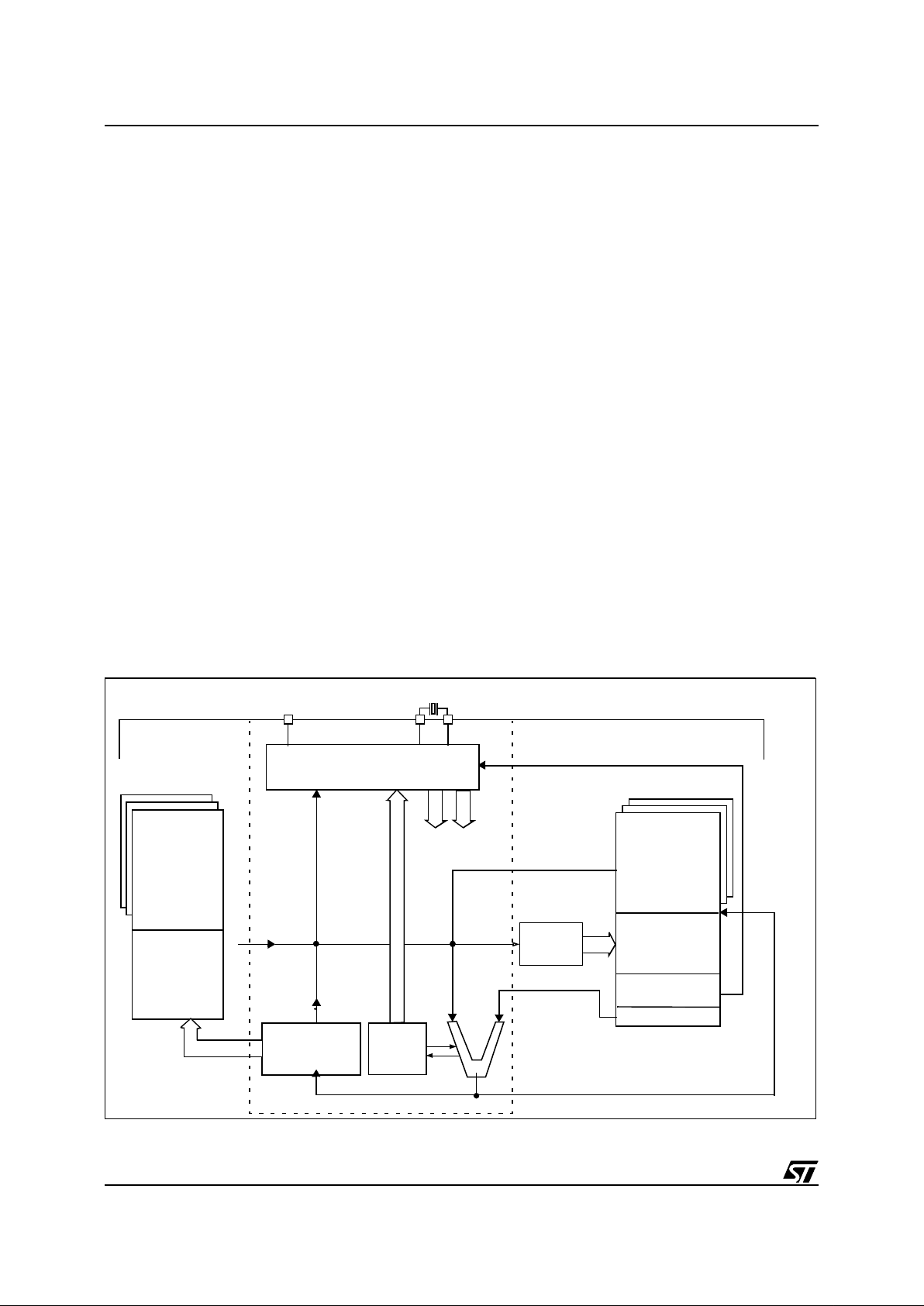
These compact low-cost devices feature a Tim er
comprising an 8-bit counter and a 7-bit programmable prescaler, an 8-bit Auto-Reload Timer,
EEPROM data capability (except ST62T52 B), an
8-bit A/D Converter with 4 analog inputs and a
Digital Watchdog timer, making them well suited
for a wide range of automot ive, appliance and industrial applications.
Figure 1. Bloc k D ia gram
TEST
NMI
INTERRUPT
PROGRAM
PC
STACK LEVEL 1
STACK LEVEL 2
STACK LEVEL 3
STACK LEVEL 4
STACK LEVEL 5
STACK LEVEL 6
POWER
SUPPLY
OSCILLATOR
RESET
DATA ROM
USER
SELECTABLE
DATA RAM
PORT A
PORT B
TIMER
DIGITAL
8 BIT CORE
TEST/V
PP
8-BIT
A/D CONVERTER
PA4..PA5 / Ain
PB0, PB2..PB3 / 20 mA Sink
V
DDVSS
OSCin OSCout RESET
WATCHDOG
MEMORY
PB6 / ARTimin / 20 mA Sink
PORT C
PC2..PC3 / Ain
AUTORELOAD
TIMER
PB7 / ARTimout / 20 mA Sink
128 Bytes
1836 bytes OTP
(ST62T52B, T62B)
1836 bytes EPROM
(ST62E62B)
DATA EEPROM
64 Bytes
(ST62T62B/E62B)
4
5/68
ST62T52B ST62T62B/E62B
1.2 PIN DESCRIPTIONS
V
DD
and V
SS
. Power is supplied to the MCU via
these two pins. V
DD
is the power connection and
VSS is the ground connection.
OSCin and OSCout.
These pins are internally
connected to the on-chip oscillator circuit. A quartz
crystal, a ceramic resonator or an exte rnal clock
signal can be connected between these two pins.
The OSCin pin is the input pin, the OSCout pin is
the output pin.
RESET
. The active-low RESET pin is used to re-
start the microcontroller.
TEST/V
PP
.
The TEST m ust be held at V
SS
for normal operation. If TEST pin is connected to a
+12.5V level during the reset phase, the
EPROM/OTP programming Mode is entered.
NMI.
The NMI pin provides the capability for asynchronous interruption, by applying an external non
maskable interrupt to the MCU. The NMI input is
falling edge sensitive. It is provided with an onchip pullup resistor and Schmitt trigger characteristics.
PA4-P A5 .
These 2 lines are organized as one I/O
port (A). Each line may be configured under software control as inputs with or without internal pullup resistors, interrupt generating in puts with pullup resistors, open-drain or push-pull outputs, analog inputs for the A/D converter.
PB0, PB2-PB3, PB6-PB7.
These 5 lines are organized as one I/O port (B). Each line may be configured under software control as inputs with or
without internal pull-up resistors, interrupt generating inputs with pull-up resistors, open-drain or
push-pull outputs. PB6/ARTIMin and PB7/ARTI-
Mout are either Port B I/O bits or the Input and
Output pins of the ARTimer.
Reset state of PB2-PB3 pins can be defined by
option either with pull-up or high impedance.
PB0, PB2-PB3, PB6-PB7 scan also sink 20mA for
direct LED driving.
PC2-PC3
. These 2 lines are organized as one I/O
port (C). Each line may be configured under software control as inpu t with or without internal pul lup resistor, interrupt generating input with pull-up
resistor, analog input for the A/D convert er, opendrain or push-pull output.
Figure 2. ST62T52B, E62B and T62B Pin
Configuration
1
2
3
4
5
6
7
89
10
11
12
13
14
15
16
PB0
V
PP
/TEST
PB2
PB3
V
DD
ARTIMin/PB6
PC2/Ain
PC3/Ain
PA5/Ain
PA4/Ain
ARTIMout/PB7
V
SS
NMI
RESET
OSCout
OSCin
5

6/68
ST62T52B ST62T62B/E62B
1.3 MEMORY MAP
1.3.1 Introduction
The MCU operates in three separate memory
spaces: Program space, Data space, and Stack
space. Operation in these three memory spaces is
described in the following paragraphs.
Briefly, Program space contains user program
code in OTP and user vectors; Data space c ontains user data in RAM and in OTP, and Stack
space accommodat es six levels of stack for subroutine and interrupt service routine nesting.
Figure 3. Me m ory A ddressing D iagram
PROGRAM SPACE
PROGRAM
INTERRUPT &
RESET VECTORS
ACCUMULATOR
DATA RAM
BANK SELECT
WINDOW SELECT
RAM
X REGISTER
Y REGISTER
V REGISTER
W REGISTER
DATA READ-ONLY
WINDOW
RAM / EEPROM
BANKING AREA
000h
03Fh
040h
07Fh
080h
081h
082h
083h
084h
0C0h
0FFh
0-63
DATA SPACE
0000h
0FF0h
0FFFh
MEMORY
MEMORY
DATA READ-ONL Y
MEMORY
6

7/68
ST62T52B ST62T62B/E62B
MEMORY MAP
(Cont’d)
1.3.2 Program Space
Program Space comprises the instructions to be
executed, the data required for immediate addressing mode instructions, the reserved factory
test area and the user vectors. Program Space is
addressed via the 12-bit Program Counter register
(PC register).
1.3.2.1 Program Memory Protection
The Program Memory in O TP or EP ROM dev ices
can be protected against external readout of
memory by selecting the READOUT PROTECTION option in the option byte.
In the EPROM parts, READOUT PROTECTION
option can be disactivated only by U.V. erasure
that also results into the whole EPROM context
erasure.
Note:
Once the Readout Protection is activated, it
is no longer poss ible, even for SGS-THOM SON,
to gain access to the OTP contents. Returned
parts with a protecti on set can therefore not be accepted.
Figure 4. ST62T52B/T62B Program
Memory Ma p
0000h
RESERVED
*
USER
PROGRAM MEMORY
(OTP/EPROM)
1836 BYTES
0F9Fh
0FA0h
0FEFh
0FF0h
0FF7h
0FF8h
0FFBh
0FFCh
0FFDh
0FFEh
0FFFh
RESERVED
*
RESERVED
INTERRUPT VECTORS
NMI VECTOR
USER RESET VECTOR
(*) Reserved areas should be filled with 0FFh
0880h
087Fh
7
8/68
ST62T52B ST62T62B/E62B
MEMORY MAP
(Cont’d)
1.3.3 Data Space
Data Space accommodates all the data necessary
for processing the user program. This space comprises the RAM res ource, the processor c ore and
peripheral registers, as well as read-only data
such as constants and look-up tables in
OTP/EPROM.
1.3.3.1 Data ROM
All read-only data is physical ly stored in program
memory, which also accommoda tes the Program
Space. The program m emory consequently contains the program code to be executed, as well as
the constants and look -up tables required by the
application.
The Data Space locations in which the different
constants and look-up tables are addressed by
the processor core may be thought of as a 64-byte
window through which it is possible to access the
read-only data stored in OTP/EPROM.
1.3.3.2 Data RAM/EEPROM
In ST62T52B, T62B and ST62E 62B devices, the
data space includes 60 bytes of RAM, the accumulator (A), the indirect registers (X), (Y), the
short direct registers (V), (W), the I/O port registers, the peripheral data an d cont rol reg isters, the
interrupt option register and the Data ROM Window register (DRW register).
Additional RAM and EEPROM pages can also be
addressed using banks of 64 bytes located between addresses 00h and 3Fh.
1.3.4 Stack Space
Stack space consists of six 12-bit registers which
are used to stack subro utine and interrupt return
addresses, as well as the current program counter
contents.
Table 1. Additional RAM / EEPROM Banks
Table 2. ST62T52B, T62B and ST62E62B Data
Memory Space
Device RAM EEPROM
ST62T52B 1 x 64 bytes ST62T62B 1 x 64 bytes 1 x 64 bytes
RAM / EEPROM banks
000h
03Fh
DATA ROM WINDOW AREA
040h
07Fh
X REGISTER 080h
Y REGISTER 081h
V REGISTER 082h
W REGISTE R 083h
DATA RAM 60 BYTES
084h
0BFh
PORT A DATA REGISTE R 0C0h
PORT B DATA REGISTE R 0C1h
PORT C DATA REGISTER 0C2h
RESERVED 0C3h
PORT A DIRECTION REGISTER 0C4h
PORT B DIRECTION REGISTER 0C5h
PORT C DIRECTION REGISTER 0C6h
RESERVED 0C7h
INTERRUPT OPTION REGISTER 0C8h*
DATA ROM WINDOW REGISTER 0C9h*
RESERVED
0CAh
0CBh
PORT A OPTION RE GI STER 0CCh
PORT B OPTION RE GI STER 0CDh
PORT C OPTION REGISTER 0CEh
RESERVED 0 CFh
A/D DATA REGISTER 0D0h
A/D CONT RO L REGISTE R 0D1h
TIMER PRESCALER REGISTER 0D2h
TIMER COUNTER REGISTER 0D3h
TIMER STATUS CONTROL REGIST ER 0D4h
AR TIMER MODE CONTROL REGISTER 0D5h
AR TIMER STATUS/CONTROL REGISTER1 0D6h
AR TIMER STATUS/CONTROL REGISTER2 0D7h
WATCHDOG REGISTER 0D8h
AR TIMER RELOAD/CAPTURE REGISTE R 0D9h
AR TIMER COMPARE REGISTER 0DAh
AR TIMER LOAD REGISTER 0DBh
OSCILLATOR CONTROL REGISTER 0DCh*
MISCELLANEOUS 0DDh
RESERVED
0DEh
0E7h
DATA RAM/EEPROM REGISTER 0E8h*
RESERVED 0E9h
EEPROM CONTROL REGISTER 0EAh
RESERVED
0EBh
0FEh
ACCUMULATOR 0FFh
* WRITE ONLY REGIST ER
8

9/68
ST62T52B ST62T62B/E62B
MEMORY MAP
(Cont’d)
1.3.5 Data Window Register (DWR)
The Data read-only memory window is located
from address 0040h to address 007Fh in Data
space. It allows direct reading of 64 consec utive
bytes located anywhere in program memory, between address 0000h and 0FFFh (top memory address depends on the specific device). All the program memory can therefore be used to store either
instructions or read-only data. Indeed, the window
can be moved in steps of 64 b ytes along t he program memory by writing the appropriate code in the
Data Window Register (DWR).
The DWR can b e addressed like any RAM location in the Data Spac e, it is howev er a write-only
register and therefore cannot be accessed using
single-bit operations. This register is used to position the 64-byte read-only data window (from address 40h to address 7Fh of the Data space) in
program memory in 64-byte steps. The ef fective
address of the byte to be read as data in program
memory is obtained by concatenating the 6 least
significant bits of the register address given in t he
instruction (as least significant bits) and the content of the DWR register (as most significant bits),
as illustrated in Figure 5 below. For instance,
when addressing location 0040h of the Data
Space, with 0 loaded in the DWR register, the
physical location addressed in program memory is
00h. The DWR register is not cleared on reset,
therefore it must be written to prior to the first access to the Data read-only memory window area.
Data Window Register (DWR)
Address: 0C9h — Write Only
Bits 6, 7 = Not used.
Bit 5-0 =
DWR5-DWR0:
Data read-only memory
Window Register Bits.
These are the Data readonly memory Window bits that correspond to the
upper bits of the data read-only memory space.
Caution:
This register is undef ine d o n res et. Ne ither read nor single bit instructions may be used to
address this register.
Note:
Care is required when ha ndling the DWR
register as it is write only. For this reason, the
DWR contents should not be changed while executing an interrupt service routine, as the service
routine cannot save and then restore the register’s
previous contents. If it is impossible to a void writing to the DWR during the interrupt service routine, an image o f the register must be saved in a
RAM location, and each time the program writes
to the DWR, it must also write to the image register. The image register must be written first so
that, if an interrupt occurs between the two i nstructions, the DWR is not affected.
Figure 5. Data read-only memory Window Memo ry Add ressi ng
70
- - DWR5 DWR4 DWR3 DWR2 DWR1 DWR0
DATA ROM
WINDOW REGISTER
CONTENTS
DATA SPACE ADDRESS
40h-7Fh
IN INSTRUCTION
PROGRAM SPACE ADDRESS
765432 0
543210
543210
READ
1
67891011
0
1
VR01573C
12
1
0
DATA SPACE ADDRESS
:
:
59h
000
0
1
00
1
11
Example:
(DWR)
DWR=28h
11
0000000
1
ROM
ADDRESS:A19h
11
13
0
1
9

10/68
ST62T52B ST62T62B/E62B
MEMORY MAP
(Cont’d)
1.3.6 Data RAM/EEPROM Bank Register
(DRBR)
Address: E8h — Write only
Bit 7-5 = These bits are not used
Bit 4 -
DRBR4
. This bit, when set, selects RAM
Page 2.
Bit 1-3. Not used
Bit 0.
DRBR0
. This bit, when set, selects EEP-
ROM page 0.
The selection of the bank is made by program-
ming the Data RAM Bank Switch register (DRBR
register) located at address E8h of the Data
Space according to Table 1. No more than one
bank should be set at a time.
The DRBR register can be addressed like a RAM
Data Space at the address E8h; nevert heless it is
a write only register that cannot be accessed with
single-bit operations. This register is used to select the desired 64-byte RAM bank of the Data
Space. The number of banks has to be loaded in
the DRBR register and the instruction has to point
to the selected location as if it was in bank 0 (from
00h address to 3Fh address).
This register is not cleared during the MCU initialization, therefore it must be written before the first
access to the Data Space bank region. Refer to
the Data Space description for additional information. The DRBR register is not modified when an
interrupt or a subroutine occurs.
Notes
:
Care is required when handling the DRBR register
as it is write only. For this reason, it is not allowed
to change the DRBR contents whi le executing interrupt service routine, as the service routine cannot save and then restore its previous content. If it
is impossible to avoid the writing of this register in
interrupt service routine, an image of this register
must be saved in a RAM lo cation, and each time
the program writes to DRBR it must write also to
the image register. The image register must be
written first, so if an interrupt occurs between the
two instructions the DRBR is not affected.
In DRBR Regis ter, only 1 bit must be set. Ot herwise two or more pages are enabled in parallel,
producing errors.
Table 3. Data RAM Bank Register Set-up
70
---
DRBR
4
---
DRBR
0
DRBR ST62T52B ST62T62B
00 None None
01 Not available EEPROM page 0
02 Not Available Not Available
08 Not available Not available
10h RAM Page 2 RAM Page 2
other Reserved Reserved
10

11/68
ST62T52B ST62T62B/E62B
MEMORY MAP
(Cont’d)
1.3.7 EEPROM Description
EEPROM memory is located in 64-byte pages in
data space. This memory may be used by the user
program for non-volatile data storage.
Data space from 00h to 3Fh is paged as described
in Table 4 . Ro w Arrangement for Pa rallel W riting
of EEPROM Locations. EEPROM locations are
accessed directly by addressing these paged sections of data space.
The EEPROM does not require dedicated instructions for rea d or write access. Once selected via the
Data RAM Bank Register, the active EEPROM
page is controlled by the EEPROM Control Re g ister (EECTL), which is described below.
Bit E20FF of the EECTL register must be reset prior
to any write or read access to the EE PR OM. If no
bank has been selected, or if E2OFF is set, any access is meaningless.
Programming must be enabled by setting the
E2ENA bit of the EECTL register.
The E2BUSY bit of the EECTL register is set when
the EEPROM is performing a program ming cycle.
Any access to the EEPR O M wh en E2BU SY is set
is meaningless.
Provided E2OFF and E2BUSY are reset, an EEPROM location is read just like any other data location, also in terms of access time.
Writing to the EEPROM may be carried out in two
modes: Byte Mode (BMODE) and Parallel Mode
(PMODE). In BMODE, one byte is acc essed at a
time, while in PMOD E up to 8 bytes in the same
row are programmed simultaneously (with consequent speed and power consumption advantages,
the latter being particularly important in battery
powered circuits).
General Notes
:
Data should be written directly to the intended address in EEPROM space. There is no buffer memory between data RAM and the EEPROM space.
When the EEPROM is busy (E2BUSY = “1”)
EECTL cannot be accessed in write mode, it is
only possible to read t he s tatus of E 2BUSY . This
implies that as long a s the EEPROM is busy, it is
not possible to change the status of the EEPROM
Control Register. EECTL bits 4 and 5 are reserved
and must never be set.
Care is required when dealing with the EECTL register, as some bits are write onl y . For this reason,
the EECTL contents must not be altered while executing an interrupt service routine.
If it is impossible to avoid writing to this register
within an interrupt service routine, an image of the
register must be saved in a RAM location, and
each time the program writes to EECTL it must
also write to the image register. T he image re gister must be written to first so that, if an interrupt occurs between the two instructions, the EECT L will
not be affected.
Table 4. . Row Arrang emen t for Para llel Writing of EEPRO M Locations
Dataspace
addresses.
Banks 0 and 1.
Byte01234567
ROW7 38h-3Fh
ROW6 30h-37h
ROW5 28h-2Fh
ROW4 20h-27h
ROW3 18h-1Fh
ROW2 10h-17h
ROW1 08h-0Fh
ROW0 00h-07h
Up to 8 bytes in each row may be programmed simultaneously in Parallel Write mode.
The number of available 64-byte banks (1 or 2) is device dependent.
11

12/68
ST62T52B ST62T62B/E62B
MEMORY MAP
(Cont’d)
Additional Notes on Parallel Mode:
If the user wishes to perform parallel programming, the first step should be to set the E2PAR2
bit. From this time on, the EEPROM will be addressed in write mode, the ROW address will be
latched and it will be possible to chan ge it only at
the end of the programming cycle, or by resetting
E2PAR2 without programming the EEPROM. After the ROW address is latched, the MCU can only
“see” the selected EEPROM row a nd any atte mpt
to write or read other rows will produce errors.
The EEPROM should not be read while E2PAR2
is set.
As soon as the E2 PAR2 bit is set, the 8 volatile
ROW latches are cleared. From this moment on,
the user can load data in all or in part of the ROW.
Setting E2PAR1 will modify the EEPROM registers corresponding to the ROW latches acces sed
after E2PAR2. For example, if the software sets
E2PAR2 and a cce sse s the EEPROM by wr i ting to
addresses 18h, 1Ah and 1Bh, and then sets
E2PAR1, these three registers will be modified simultaneously; the remaining bytes in the row will
be unaffected.
Note that E2PAR2 is internally reset at t he en d of
the programming cycle. This implies that the user
must set the E2PAR2 bit between two parallel programming cycles. Note that if the user tries to set
E2PAR1 while E2PAR2 is not set, there will be no
programming cycle and the E2PAR1 bit will be unaffected. Consequently, the E2PAR1 bit cannot be
set if E2ENA is low. The E2PAR1 bit can be set by
the user, only if the E2ENA and E2PAR2 bits are
also set.
EEPROM Control Regi s t e r (EEC T L)
Address: EAh — Read/Write
Reset status: 00h
Bit 7 = D7:
Unused.
Bit 6 =
E2OFF
:
Stand-by Enable Bit.
WRIT E ON LY.
If this bit is set the EEPROM is disabled (any access
will be meaningless) and the power consumption of
the EEPROM is reduced to its lowest value.
Bit 5-4 =
D5-D4
:
Reserved.
MUST be kept reset.
Bit 3 =
E2PAR1
:
Parallel Start Bit.
WRITE ONLY.
Once in Parallel Mode, as soon as the user software
sets the E2PAR1 bit, parallel writing of the 8 adjacent registers will start. This bit is internally reset at
the end of the programm ing procedure. Not e that
less than 8 bytes can be written if required, the undefined bytes being unaffected by the parallel programming cycle; this is explained in greater detail
in the Additional Notes on Parallel Mode overleaf.
Bit 2 =
E2PAR2
:
Parallel Mode En. Bit.
WRITE
ONLY. This bit must be set by the user program in
order to perform parallel programming. If E2PAR2
is set and the parallel start bit (E2PAR1) is reset,
up to 8 adjacent bytes can be written simultaneously. These 8 adjacent bytes are considered as a
row, whose addres s lines A7, A6, A5, A 4, A3 are
fixed while A2, A1 and A0 are the chan ging bits,
as illustrated in Table 4. E2PAR2 is automatical ly
reset at the end of any parallel progra mming procedure. It can be reset by the user software before
starting the programming procedure, thus leaving
the EEPROM registers unchanged.
Bit 1 =
E2BUSY
:
EEPROM Busy Bit.
READ ONLY. This bit is automatically set by the EEPROM
control logic when the EEPROM is in programming mode. Th e user program should test it before any EEPROM read or write operation; any attempt to access the EEPRO M while the busy bit is
set will be aborted and the writing procedure in
progress will be completed.
Bit 0 =
E2ENA
:
EEPROM Enable Bit.
WRITE ONLY. This bit enables programming of the EEPROM
cells. It must be s et before any write to the EEPROM register. Any attempt to write to the EEPROM when E2ENA i s low is m eanin gless and will
not trigger a write cycle.
70
D7
E2O
FF
D5 D4
E2PAR1E2PAR2E2BUSYE2E
NA
12

13/68
ST62T52B ST62T62B/E62B
1.4 PROGRAMMING MODES
1.4.1 Option Byte
The Option B yte all o ws conf igurat ion capability to
the MCUs. Option byte’s content is automatically
read, and the selected options enabled, whe n the
chip reset is activated.
It can only be acces sed during the programming
mode. This access is made either automatically
(copy from a master device) or by selecting the
OPTION BYTE PROGRAMMING mode of the
programmer.
The option byte is located in a non-user map. No
address has to be specified.
EPROM Code Option Byte
PROTECT
. This bit allows the protection of the
software contents against piracy. When the bit
PROTECT is se t high, readout of the OTP contents is prevented by hardware. No programming
equipment is able to gain access to the user program. When this bit is low, the user program can
be read.
EXTCNTL
. This bit selects the External STOP
Mode capability. When EXTCNTL is high, pin NMI
controls if the STOP mode can be accessed when
the watchdog is active. When EXTCNTL is low,
the STOP instruction is processed as a WAIT as
soon as the watchdog is active.
PB2- 3 P UL L
. When set this bit removes pull-up at
reset on PB2-PB3 pins. When cleared PB2-PB3
pins have an internal pull-up resistor at reset.
D4
. Reserved. Must be cleared to zero.
WDACT
. This bit controls the watchdog activation.
When it is high, hardware activation is sel ected.
The software activation is sel ected when W D AC T
is low.
DELAY
. This bit enables the selection of the delay
internally generated after pin RESET is released.
When DELAY is low, the delay is 2048 cycles of
the oscillator, it is of 32768 cycles when DELAY is
high.
OSCIL
. When this bit is low, the oscillator must be
controlled by a quartz crystal, a ceramic resonator
or an external frequency. When it is high, the oscillator must be controlled by an RC ne twork, with
only the resistor having to be externally provided.
D0
. Reserved. Must be cleared to zero.
The Option byte is written during programming either by using t he PC menu (PC driven Mode) or
automatically (stand-alone mode)
1.4.2 Program Memory
EPROM/OTP programming mode is set by a
+12.5V voltage appl ied to the TE ST/V
PP
pin. The
programming flow of the ST62T62B is described
in the User Manual of the EP ROM Programming
Board.
The MCUs can be programmed with the
ST62E6xB EPROM programming tools available
from SGS-THOMS ON.
Table 5. ST62T52B/T62B Program Memory Map
Note
: OTP/EPROM dev ices can be programme d
with the development tools available from
SGS-THOMSON (ST62E6X-EPB or
ST626X-KIT).
1.4.3 . EEPROM Data Memory
EEPROM data pages are supplied in the virgin
state FFh. Partial or total programming of EEPROM data memory can be performed either
through the application software or through an external programmer. Any SGS-THOMSON tool
used for the program memory (OTP/EPROM) can
also be used to program the EEPROM data memory.
70
PROTECT
EXTC-
NTL
PB2-3
PULL
- WDACT DELAY OSCIL -
Device Address Description
0000h-087Fh
0880h-0F9Fh
0FA0h-0FEFh
0FF0h-0FF7h
0FF8h-0FFBh
0FFCh-0FFDh
0FFEh-0FFFh
Reserved
User ROM
Reserved
Interrupt Vectors
Reserved
NMI Interrupt Vector
Reset Vector
13
14/68
ST62T52B ST62T62B/E62B
2 CENTRAL PR OCESSING UNIT
2.1 INTRODUCTION
The CPU Core of ST6 devices is independent of
the I/O or Memory configuration. As such, it may be
thought of as an independent central processor
communicating with on-chip I/O, M emory and Peripherals via internal address, data, and control
buses. In-core communication is arranged as
shown in Figure 6; the controller being externally
linked to both the Reset and Oscillator circuits,
while the core is linked to the dedicated on-chip peripherals via the serial data bus and indirectly, for
interrupt purposes, through the control registers.
2.2 CPU REGISTERS
The ST6 Family CPU core features six registers and
three pairs of flags available to the programmer.
These are described in the following paragraphs.
Accumulator (A)
. The accumulator is an 8-bit
general purpose register used in all arithmetic calculations, logical operations, and data manipulations. The accumulator can be addressed in Data
space as a RAM l ocation at address FFh. Thus
the ST6 can manipulate the ac cumulator just like
any other register in Data space.
Indirect Registers (X, Y).
These two indirect registers are used as pointers to memory locations in
Data space. They are used i n the regist er-indirect
addressing mode. These registers can be addressed in the data space as RAM locations at addresses 80h (X) and 81h (Y). They can also be accessed with the direct, short direct, or bit direct addressing modes. Accordingly, the ST6 instruction
set can use the indirect registers as any other register of the data space.
Short Direct Registers (V, W).
These two registers are used to save a byte in short direct addressing mode. T hey can be addressed in Data
space as RAM locations at addresses 82h (V) and
83h (W). They can also be accessed using the direct and bit direct addressing modes. Thus, the
ST6 instruction set can use the sho rt direct registers as any other register of the data space.
Program Counter (PC). The program cou nter is a
12-bit register which contains the address of the
next ROM location to be process ed by the core.
This ROM location may be an opcode, an operand, or the address of an operand. The 12-bit
length allows the direct addressing of 4096 bytes
in Program space.
Figure 6ST6 Core Block Diagram
PROGRAM
RESET
OPCODE
FLAG
VALUES
2
CONTROLLER
FLAGS
ALU
A-DATA
B-DATA
ADDRESS/READ LINE
DATA SPACE
INTERRUPTS
DATA
RAM/EEPROM
DATA
ROM/EPROM
RESULTS TO DATA SPACE (WRITE LINE)
ROM/EP ROM
DEDICA T I ONS
ACCUMULATOR
CONTRO L
SIGNALS
OSCin
OSCout
ADDRESS
DECODER
256
12
Program Co unter
and
6 LAYER STACK
0,01 TO 8MHz
VR01811
14

15/68
ST62T52B ST62T62B/E62B
CPU REGISTERS
(Cont’d)
However, if the program space contains more
than 4096 bytes, the additional memory in program space can be address ed by using the Program Bank Switch register.
The PC value is incremented after reading the address of the current instruction. To execute relative jumps, the PC and the offset are shifted
through the ALU, where they are added; the result
is then shifted back into the PC. The program
counter can be changed in the following ways:
- JP (Jump) instructionPC=Jump address
- CALL instructionPC= Call address
- Relative Branch Instruction.PC= PC +/- offset
- Interrupt PC=Interrupt vector
- ResetPC= Reset vector
- RET & RETI instructionsPC= Pop (stack)
- Nor mal in structio nPC= PC + 1
Flags (C, Z)
. The ST6 CPU includes three pairs of
flags (Carry and Zero), each pair being associated
with one of the three normal modes of operat ion:
Normal mode, Interrupt mode and Non Maskable
Interrupt mode. Each pair consists of a CARRY
flag and a ZERO flag. One pair (CN, ZN) is used
during Normal operation, another pair is used during Interrupt mode (CI, ZI), and a third pair is used
in the Non Maskable Interrupt mode (CNMI, ZNMI).
The ST6 CPU uses the pair of flags associated
with the current mode: as soon a s an in terrupt (or
a Non Maskable Interrupt) is generated, the ST 6
CPU uses the Interrupt flags (resp. the NMI flags)
instead of the Normal flags. When the RETI instruction is executed, the previously used set of
flags is restored. It should be no ted tha t eac h flag
set can only be addressed in its own context (Non
Maskable Interrupt, Normal Interrupt or M ain routine). The flags are not cleared during context
switching and thus retain their status.
The Carry flag is set when a carry or a borrow occurs during arithmetic operations; otherwise it is
cleared. The Carry flag is al so set to the value of
the bit tested in a bit test instruction; it also participates in the rotate left instruction.
The Zero flag is set if the result of the last arithmetic or logical operation was equal to zero; otherwise it is cleared.
Switching between the three sets of flags is performed automatically when an NMI, an interrupt or
a RETI instructions occurs. As the NMI mode is
automatically selected after the reset of the M CU,
the ST6 core uses at first the NMI flags.
Stack.
The ST6 CPU includes a true LIFO hardware stack which elim inates the need for a stack
pointer. The stack consists of six separate 12-bit
RAM locations that do not belong to the data
space RAM area. When a subroutine call (or in terrupt request) occurs, the contents of each level
are shifted into the next higher level, while the
content of the PC is shifted into the first level (the
original contents of the sixth stack level are lost).
When a subroutine or interrupt return occurs (RET
or RETI instructions), the first level register is shifted back into the PC and the value o f each le vel is
popped back into the previous level. Since the accumulator, in common with all other data space
registers, is not stored in this stack, management
of these registers should be performed within the
subroutine. The st ack will remain in its “deepest”
position if more than 6 nested calls or interrupts
are executed, and consequently the last return address will be lost. It will also remain in its highest
position if the stack is empty and a RET or RETI is
executed. In this case the next instruction will be
executed.
Figure 7ST6 CPU Programmi ng Mode
l
SHORT
DIRECT
ADDRESSING
MODE
VREGISTER
WREGISTER
PROGRAM COUNTER
SIX LEVELS
ST ACK REGI STER
CZNORMAL FLAGS
INTERRUPT FLAGS
NMI FLAGS
INDEX
REGISTER
VA 000423
b7
b7
b7
b7
b7
b0
b0
b0
b0
b0
b0b11
ACCUMULATOR
Y R EG. POINTER
X R EG. POINTER
CZ
CZ
15

16/68
ST62T52B ST62T62B/E62B
3 CLOCKS, RESET, INTER RUPTS AND POWER SAVIN G MO DES
3.1 CLOCK SYSTEM
The MCU features a Main Oscillator which can be
driven by an external clock, or used in conjunction
with an AT-cut parallel resonant crystal or a suitable ceramic resonator, or with an external resistor
(R
NET
).
Figure 8. illustrates various possible oscillator con-
figurations using an external crystal or ceramic resonator, an external clock input, an external resistor
(R
NET
). CL1 an CL2 should have a capacitance in the
range 12 to 22 pF for an oscillator frequency in the
4-8 MHz range.
A programmable divider is provided in order to adjust
the internal clock of the MCU to the best power consumption and performance trade-off.
The internal MCU clock frequency (f
INT
) drives directly the AR TIMER while it is divided by 12 to
drive the TIMER, the A/D converter and the
Watchdog timer, and by 13 to drive the CPU core,
as may be seen in Figure 9..
With an 8MHz oscillator frequency, the fastest
machine cycle is therefore 1.625µs.
A machine cycle is the smal lest unit of time needed
to execute any operation (for instance, to increment
the Program Counter). An inst ruction m ay req uire
two, four, or five machine cycles for execution.
3.1.1 Main Oscillator
The oscillator configuration may be specified by selecting the appropriate option. When the CRYSTAL/RESONATOR option is selected, it must be
used with a quartz crystal, a cerami c resonat or or
an external signal provided on the OSCin pin. When
the RC NETWORK option is selected, the system
clock is generated by an external resistor.
Figure 8. Oscillator Configurations
OSC
in
OSC
out
C
L1n
C
L2
ST6xxx
CRYSTAL/RESO NATOR CL O CK
CRYSTAL/RESONATOR option
OSC
in
OSC
out
ST6xxx
EXTERNAL CLOCK
CRYSTAL/RESONATOR option
NC
OSC
in
OSC
out
R
NET
ST6xxx
RC NETWORK
RC NETW O RK option
NC
16

17/68
ST62T52B ST62T62B/E62B
CLOCK SYSTEM
(Cont’d)
Oscillator Control Registers
Address: DCh — Write only
Bit 7-4. These bits are not used.
Bit 3. Reserved. Cleared at Reset. THIS BIT
MUST BE SET TO 1 BY USER PROGRAM to
achieve lowest power consumption.
Bit 2. Reserved. Must be kept low.
RS1-RS0. These bits select the division ratio of
the Oscilla tor Divide r in order to genera te the internal frequency. The following selctions are available:
Note
: Care is required when handling the OSCR
register as some bits are wri te only. For this reason, it is not allowed to change the OSCR contents while executing interrupt service rout ine, as
the service routine cannot save and t hen restore
its previous content. If it is impossible to avoid the
writing of this register in inte rrupt service routine,
an image of this register mus t be s aved i n a RA M
location, and each time the program writes to
OSCR it must write also to the image register. The
image register must be writte n first, so if an interrupt occurs between the two instructions the
OSCR is not affected.
Figure 9. Clo ck Cir c ui t Block Diagram
70
----
OSCR3OSCR
2
RS1 RS0
RS1 RS0 Division Ratio
0
0
1
1
0
1
0
1
1
2
4
4
MAIN
OSCILLATOR
Core
:
13
:
12
:
1
Timer
Watchdog
POR
f
INT
ADC
AR Timer
OSCILLATOR
DIVIDE R
RS0, RS1
OSCin
OSCout
f
OSC
f
OSC
17

18/68
ST62T52B ST62T62B/E62B
3.2 RESETS
The MCU can be reset in three ways:
– by the external Reset input being pulled low;
– by Power-on Reset;
– by the digital Watchdog peripheral timing out.
3.2.1 RESET Input
The RESET
pin may be c onnected to a device of
the application board in order to reset t he M CU if
required. The RESET
pin may be pulled low in
RUN, WAIT or STOP mode. This input can be
used to reset the MCU internal state and ensure a
correct start-up procedure. The pin is ac tive low
and features a Schmitt trigger input. The i nternal
Reset signal is generated by adding a delay to the
external signal. Therefore even short pulses on
the RESET
pin are acceptable, p rovided VDD has
completed its rising phase and that the oscillator is
running correctly (normal RUN or WAIT modes).
The MCU is kept in the Reset state as long as the
RESET
pin is held low.
If RESET
activatio n occ urs in the RU N or WAIT
modes, processing of the user program is stopped
(RUN mode only), the Inputs and Outputs are configured as inputs with pull-up resistors and the
main Oscillator is restarted. When the level on the
RESET pin then goes high, the initialization sequence is executed following expiry of the internal
delay period.
If RESET
pin activation occurs in the STOP mode,
the oscillator starts up and all I nputs and O utputs
are configured as inputs with pull-up resistors.
When the level of the RESET
pin then goes high,
the initialization sequence is executed following
expiry of the internal delay period.
3.2.2 Power-on Reset
The function of the POR circuit consists in waking
up the MCU at an appropriate stage during the
power-on sequence. At the beginning of this sequence, the MCU is configured in the Reset state:
all I/O ports are configured as inputs with pull-up
resistors and no instruction is executed. When the
power supply voltage rises to a sufficient level, the
oscillator starts to operate, whereupon an inte rnal
delay is initiated, in order to allow the oscillator to
fully stabilize before executing the first instruction.
The initialization sequence is executed immediately following the internal delay.
The internal delay is generated by an on-chip counter. The internal reset line is released 2048 internal
clock cycles after release of the external reset.
Notes:
To ensure correct start-up, the user shou ld take
care that the reset signal is not released before
the V
DD
level is su ffic ient to allow MC U ope ratio n
at the chosen frequ ency (see Rec om me nded O perating Conditions).
A proper reset sig nal f or a s lo w ri sing V
DD
supply
can generally be provided by an external RC network connected to the RESET
pin.
Figure 10. Reset and Interrupt Processing
INT LATCH CLEARED
NMI MASK SET
RESET
( IF PRESENT )
SELECT
NMI MODE FLAGS
IS RESET STILL
PRESENT?
YES
PUT FFEH
ON ADDRESS BUS
FROM RESET LOCATIO NS
FFE/FFF
NO
FETCH INSTRUCTI ON
LOAD PC
VA000427
18

19/68
ST62T52B ST62T62B/E62B
RESETS
(Cont’d)
3.2.3 Watchdog Reset
The MCU provides a Watchdog timer function in
order to ensure graceful recovery from software
upsets. If the Watchdog register is not refreshed
before an end-of -count condition is reached, the
internal reset will be activated. This, amongst other things, resets the watchdog counter.
The MCU restarts just as though the Reset had
been generated by the RESET
pin, including the
built-in stabilisation delay period .
3.2.4 Application Notes
No external resistor is required between V
DD
and
the Reset pin, thanks to the built-in pull-up device.
The POR circuit operates dynamically, in that it
triggers MCU init ialization on detec ting the rising
edge of V
DD
. The typical threshold is in the region
of 2 volts, but the actual value of the detected
threshold depends on the way in which V
DD
rises.
The POR circuit is
NOT
designed to supervise
static, or slowly rising or falling V
DD
.
3.2.5 MCU Initialization Sequence
When a reset occurs the s tack is reset, the PC is
loaded with the address of the Reset Vector (located in program ROM starting at address
0FFEh). A jump to the begin ning of the user program must be coded at this address. Fo llowing a
Reset, the Interrupt flag is automatically set, so
that the CPU is in Non Maskable In terrupt mode;
this prevents the initialisation routine from being
interrupted. The initialisation routine should therefore be terminated by a RETI instruction, in order
to revert to normal mode a nd enable interrupts. If
no pending interrupt is present at the end of the initialisation routine, the MCU will continue by
processing the instruction immediately following
the RETI instruction. If, however, a pending interrupt is present, it will be serviced.
Figure 11. Reset and Interrupt Processing
Figure 12. Reset Block Diagram
RESET
RESET
VECTOR
JP
JP:2 BYTES/4 CYCLES
RETI
RETI: 1 BYTE/2 CYCLES
INITIALIZATION
ROUTINE
VA00181
V
DD
RESET
300k
Ω
2.8k
Ω
POWER
WATCHDOG RESET
CK
COUNTER
RESET
ST6
INTERNAL
RESET
f
OSC
RESET
ON RESET
VA0200B
19

20/68
ST62T52B ST62T62B/E62B
RESETS
(Cont’d)
Table 6. Register Reset Status
Register Address(es) Status Comment
Oscillator Control Register
EEPROM Control Register
Port Data Registers
Port Direction Register
Port Option Register
Interrupt Option Register
TIMER Status/Control
AR TIMER Mode Control Register
AR TIMER Status/Control 1 Register
AR TIMER Status/Control 2Register
AR TIMER Compare Register
Miscellaneous Register
0DCh
0EAh
0C0h to 0C2h
0C4h to 0C6h
0CCh to 0CEh
0C8h
0D4h
0D5h
0D6h
0D7h
0DAh
0DDh
00h
f
INT
= f
OSC
; user must set bit3 to 1
EEPROM enabled (if available)
I/O are Input with pull-up
I/O are Input with pull-up
I/O are Input with pull-up
Interrupt disabled
TIMER disabled
AR TIMER stopped
X, Y, V, W, Register
Accumulator
Data RAM
Data RAM Page REgister
Data ROM Window Register
EEPROM
A/D Result Register
AR TIMER Load Register
AR TIMER Reload/Capture Register
080H TO 083H
0FFh
084h to 0BFh
0E8h
0C9h
00h to F3h
0D0h
0DBh
0D9h
Undefined
As written if programmed
TIMER Counter Register
TIMER Prescaler Register
Watchdog Counter Register
A/D Control Register
0D3h
0D2h
0D8h
0D1h
FFh
7Fh
FEh
40h
Max count loaded
A/D in Standby
20

21/68
ST62T52B ST62T62B/E62B
3.3 DIGITAL WATCHDOG
The digital Watchdog consists of a reloadable
downcounter timer which can be used to provide
controlled recovery from software upsets.
The Watchdog circuit generates a Reset when the
downcounter reaches zero. User software can
prevent this reset by reloading the counter, and
should therefore be written so that the counter is
regularly reloaded while the user program runs
correctly. In the event of a software misha p (usually caused by externally generated interference),
the user program will no longer behave in its usual
fashion and the timer register will thus not be reloaded periodically. Consequently the timer will
decrement down to 00h and reset the MCU. In order to maximise the effectiveness of the Watchdog function, user software must be written with
this concept in mind.
Watchdog behaviour is governed by two options,
known as “WATCHDOG ACTIVATION” (i.e.
HARDWARE or SOFTWARE) and “EXTERNAL
STOP MODE CONTROL” (see Table 7 Recom-
mended Option Choices).
In the SOFTWARE option, the Watchdog is disabled until bit C of the DWDR register has been set.
When the Watchdog is disabled, low power Stop
mode is available. Once activated, the Watchdo g
cannot be disabled, except by resetting the MCU.
In the HARDWARE option, t he Watchdog is permanently enabled. Since the oscillator will run
continuously, low power mode is not available.
The STOP instruction is interpreted as a WAIT instruction, and the Watchdog continues to countdown.
However, when the EXTERNAL STOP MODE
CONTROL option has been selected low power
consumption may be achieved in Stop Mode.
Execution of the STOP instruction is then governed by a secondary function associated with the
NMI pin. If a STOP instruction is encountered
when the NMI pin is low, it is interpreted as WAIT,
as described above. If, however, the STOP instruction is encountered when the NMI pin is high,
the Watchdog counter is frozen and the CPU enters STOP mode.
When the MCU exits STOP mode (i.e. when an interrupt is generated), the Watchdog resumes its
activity.
Table 7. Recommended Option Choices
Functions Required Recommended Options
Stop Mode & Watchdog “EXTERNAL STOP MODE” & “HARDWARE WATCHDOG”
Stop Mode “SOFTWARE WATCHDOG”
Watchdog “HARDWARE WATCHDOG”
21
 Loading...