

1/12March 2002
■ DUAL INPUT VOLTAGE (12V AND 5V)
■ TRIPLE OUTPUT VOLTAGE (2.6V, 3.3V, 8V)
■ 2.6V GUARANTEED I
OUT
UP TO 1.2A
■ 3.3V GUARANTEED I
OUT
UP TO 1.0A
■ 8V GUARANTEED I
OUT
UP TO 200mA
■ THERMAL AND SHORT CIRCUIT
PROTECTION
■ GUARANTEED OPERATING
TEMPERATURE RANGE (0°C to 125°C)
DESCRIPTION
This device contains three voltage regulators, all
fixed output voltage, in one 7 pin surface mount
package. The first is a 2.6 V regulator to power the
integrated controller/µP. The second is a 3.3V
regulator to power the read channel chip, and
memory chips requiring 3.3V The last is an 8V
regulator to power the preamp chip. The bandgap
reference, the 8V ground, and the substrate are all
tied to a common groun d pin, while the 2.6V and
3.3V ground is tied to a separate ground pin.This
grounding scheme allows for improved noise
isolation between the 8V reg ulator and the 2.6V
and 3.3V regulators.The 2.6V and 3.3V regulators
shall be respectively capable of 1.0A and 1.2A.
The 8V regulator shall be capable of 200mA.
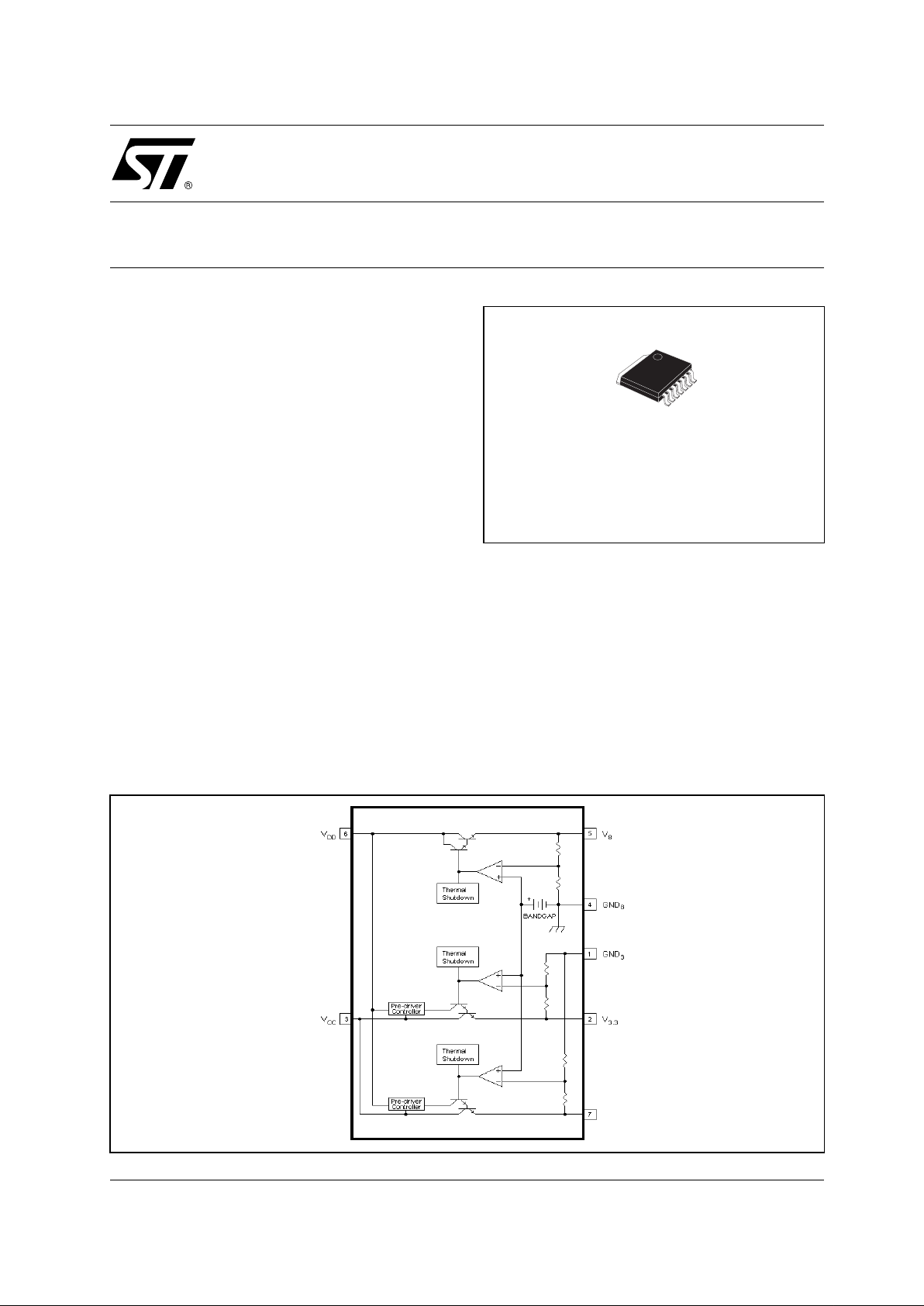
It is housed in the SPAK (PowerFlex)
ST3L01
TRIPLE VOLTAGE REGULATOR
V
2.6
SCHEMATIC DIAGRAM
SPAK-7L
(PowerFlex
)
ST3L01
2/12
ABSOLUTE MAXIMUM RATINGS
GENERAL OPERATING CONDITION
THERMAL DATA
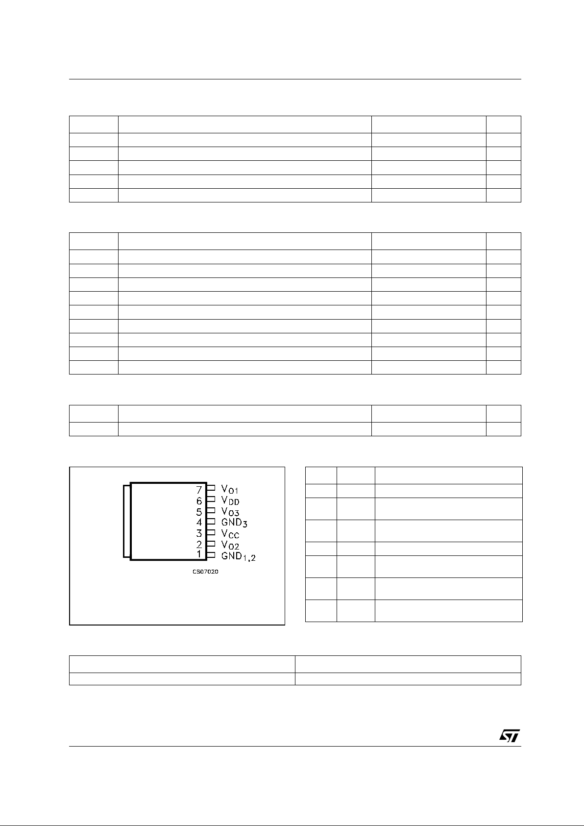
CONNECTION DIAGRAM (top view) PIN DESCRIPTION
ORDERING INFORMATION
(*) Avai l abl e in Tape & Reel wi th the suffix " R"
Symbol Parameter Value Unit
V
CC
Supply Voltage
18 V
V
DD
ISupply Voltage
18 V
V
ESD
ESD Tolerance (Human Body Model)
4KV
T
stg
Storage Temperature Range
-65 to +150 °C
T
J
Operating Junction Temperature Range
0 to +150 °C
Symbol Parameter Value Unit
V
CC
VCC Supply Voltage
4.75 to 5.25 V
∆V
CC
VCC Ripple
±0.15 V
t
r
Rise Time (10% to 90%) referred to V
CC
1V
t
f
Fall Time (90% to 10%) referred to V
CC
1V
V
DD
VDD Supply Voltage
10.8 to 13.2 V
∆V
DD
VDD Ripple
±0.3 V
t
r
Rise Time (10% to 90%) referred to V
DD
1V
t
f
Fall Time (90% to 10%) referred to V
DD
1V
T
Al
Operating Ambient Temperature Range
0 to 70 µs
Symbol Parameter SPAK-7L Unit
R
thj-case
Thermal Resistance Junction-case
2 °C/W
SPAK-7L
Pin N° Symbol Name and Function
1 GND
1,2VO1
and VO2 regulators GND pin
2V
O2
Second Output Pin: Bypass with a
0.1µF capacitor to GND
3V
CC
Input Pin: Bypass with a 0.1µF
capacitor to GND
4GND
3
VO3 regulators GND pin
5V
O3
Third Output Pin: Bypass with a
0.1µF capacitor to GND
6V
DD
Input Pin: Bypass with a 0.1µF
capacitor to GND
7V
O1
First Output Pin: Bypass with a 0.1µF
capacitor to GND
TYPE SPAK (Power Flex) 7 leads (*)
ST3L01 ST3L01K7

ST3L01
3/12
TYPICAL APPLICATION CIRCUIT
Note: To i m prove noise figure of the 8V VREG connect this capacitor to the GND8V pin. CCC, CDD, CO1, CO2 and CO3 capa citors mu st be
locate d not more than 0.5" from the output pins of the de vice. Form mo re details about Capacitors read the "Appl i cation Hints"
ELECTRICAL CHARACTERISTICS (VCC=5V, VDD=12V, CCC=1µF (Tantalum), CDD=0.1µF (X7R),
C
O1=CO2=CO3
=0.11µF (X7R) Tj=0 to 125°C unless otherwise specified. Typical values are referred at
T
j
=25°C, I
FL1
=1.2A, I
FL2
=1.0A, I
FL3
=0.2A,
Symbol Parameter Test Conditions Min. Typ. Max. Unit
V
O1
Output Voltage 1 IO1 = 10mA Tj = 25°C 2.575 2.6 2.626 V
I
O1
= 0 to I
FL1
VCC = 4.75 to 5.25V
T
j
= 0 to 125°C
2.55 2.6 2.65
V
DD
= 0 to 10.8V IO1 = 0.5A 2.2 2.65
V
O2
Output Voltage 2 IO2 = 10mA Tj = 25°C 3.23 3.3 3.37 V
I
O2
= 0 to I
FL2
VCC = 4.75 to 5.25V
T
j
= 0 to 125°C
3.2 3.3 3.4
V
DD
= 0 to 10.8V IO2 = 0.5A 2.92 3.4
V
O3
Output Voltage 3 IO3 = 10mA Tj = 25°C 7.84 8 8.16 V
I
O3
= 0 to I
FL3
VDD = 10.8 to 13.2V
T
j
= 0 to 125°C
7.76 8 8.24
∆V
O
Line Regulation 1 IO = 10mA VCC =±5% VDD =±10% <0.2 %V
O
∆V
O
Load Regulation 1 IO = 0.01 to IFL (Note 1) <0.4 %V
O
V
D1
Dropout Voltage 1 IO1 = I
FL1
(Note 2) 1.3 1.9 V
V
D2
Dropout Voltage 2 IO2 = I
FL2
(Note 2) 1.13 1.4 V
V
D3
Dropout Voltage 3 IO3 = I
FL3
(Note 2) 1.6 2.2 V
t
TR
Transient Response (Note 3, 7) <1 µs
I
OL1
Output 1 Current Limit ∆VO = 125mV 1.5 2.1 2.5 A
I
OL2
Output 2 Current Limit ∆VO = 165mV 1.1 1.7 2.5 A
I
OL3
Output 3 Current Limit ∆V
OUT
= 400mV 0.25 0.4 0.5 A
I
O1
Output 1 Minimum Load
Current
(Note 4, 7) 0 mA
I
O2
Output 2 Minimum Load
Current
(Note 4, 7) 0 mA
I
O3
Output 3 Minimum Load
Current
(Note 4, 7) 0 mA

ST3L01
4/12
Note 1: Low duty cycle pul se testing with Kelvin connections are required in ord er to maintain accurate data
Note 2: Dropout Voltage is defined as the minimum differential voltage between V
I
and VO requir ed to m anta in re gulat ion at VO. It is measured
when the output voltage drops 100mV below its nominal value.
Note 3: Transient respo nse is defined w i th a st ep change in load from 10mA to I
FL
/2 as the time f rom the load ste p until the output voltage
reaches it’s minimum value.
Note 4: Min i m um lo ad current is defined as the minimum cu rrent required at the output in order to mai ntain regulation for the output voltage.
Note 5: The regulator shall withstand 100000 reverse bias discharges of the maxim um output capaci tance, with no d egradation, when the
input voltage is switched to ground in 1 µs.
Note 6: Temperature stability is the change in output from nominal over the operating temperature range.
Note 7: Guaranteed by design, not tested in production.
APPLICATION HINTS
EXTERNAL CAPACITORS
The ST3L01 requires external capacitors for
stability. We sugge st to sol der both ca pacitors as
close as possible to the relative pins.
INPUT CAPACITORS
An input capacitor, whose value is at least 0.1µF,
is required on the V
DD
input; the amount of the
input capacitance can be increased without limit.
Any good quality tantalum or ceramic low ESR
capacitor may be used at the V
DD
input.
Any input capacitor, whose value is at least 1
m
F is
instead required on the V
CC
input; the amount of
this input capacitance can be increased without
limit. Tantalum or aluminum electrolitic capacitor
can be used at the V
CC
input; ceramic, low ESR
capacitor are not recommended.
Both capacitors must be located at a distance of
not modre than 0.5" from the input pins of the
device and returned to a clean analog ground.
OUTPUT CAPACITOR
The ST3L01 is designed specifically to work with
Ceramic and Tantalum capacitors.
The test results of the ST3L01 stability using
multilayer ceramic capacitors show that a
minimum value of 0.1µF is needed for the three
regulators. This value can be increased for even
better transient response and noise performance.
Surface-mountable solid tantalum capacitors offer
a good combination of small physical size for the
capacitance value a nd ESR in the ran ge nee d by
the ST3L01. The test results show good stability
for both outputs with values of at least 0.1µF. Also
this capacitor value can be increased without limit
for even better performance such a transient
response and noise.
IMPORTANT; The output capacitor must maintain
its ESR in the stable region over the full operating
temperature to assure stability. Also , capacitor
tolerance and variation with temperature must be
considered to assure that the minimum amount of
capacitance is provided at all times. For this
reason, when a caramic multilayer capacitor is
used, the better choise for temperatu re coefficent
is the X7R type, which holds the capacitance
within ±15% . The output capacitor should be
located not more than 0.5" from the ou tput pins of
the device and returned to a clean analog ground.
C
O
Output Capacitor (Note 5, 7) 0.1 µF
C
CC
Input Capacitor (Note 5) 1.0 µF
C
DD
Input Capacitor (Note 5) 0.1 µF
Reg
Therm
Therma Regulation I
OUT
= IFL, t
PULSE
= 30ms (Note 7) 0.1 0.3 %/W
SVR1 Supply Voltage Rejection
(V
CC
to Output 1)
B = 100Hz to 100KHz I
O1
= I
FL1
/10
V
CC
= 4.75 to 5.25V (Note 7)
30 >40 dB
SVR2 Supply Voltage Rejection
(V
CC
to Output 2)
B = 100Hz to 100KHz I
O2
= I
FL2
/10
V
CC
= 4.75 to 5.25V (Note 7)
30 >40 dB
SVR3 Supply Voltage Rejection
(V
DD
to Output 3)
B = 100Hz to 100KHz I
O3
= I
FL3
/10
V
DD
= 10.8 to 13.2V (Note 7)
40 >50 dB
I
VCC
VCC Quiescent Current IO1 = IO2 = IO3 = 0 7 10 mA
I
VDD
VDD Quiescent Current IO1 = IO2 = IO3 = 0 13 20 mA
eN Output Noise B = 10Hz to 10KHz (Note 7) 0.003 %V
OUT
∆V
O
Temperature Stability IO = 10mA (Note 6, 7) 0.5 %V
OUT
∆V
O
Long Term Stability Tj = 125°C, 1000Hrs (Note 7) 0.3 %V
OUT
Symbol Parameter Test Conditions Min. Typ. Max. Unit

ST3L01
5/12
TYPICAL CHARACTERISTICS (CCC=1µF (tant), CDD=100nF (X7R), All CO=100nF (X7R))
Figure 1 : Output Voltage vs Temperature
Figure 2 : Output Voltage vs Temperature
Figure 3 : Output Voltage vs Temperature
Figure 4 : Load Regulation vs Temperature
Figure 5 : Load Regulation vs Temperature
Figure 6 : Load Regulation vs Temperature

ST3L01
6/12
Figure 7 : Dropout Voltage vs Temperature
Figure 8 : Dropout Voltage vs Temperature
Figure 9 : Dropout Voltage vs Temperature
Figure 10 : Dropout Voltage vs Output Current
Figure 11 : Dropout Voltage vs Output Current
Figure 12 : Dropout Voltage vs Output Current

ST3L01
7/12
Figure 13 : Current Limit vs Temperature
Figure 14 : Current Limit vs Temperature
Figure 15 : Current Limit vs Temperature
Figure 16 : Output Voltage vs Output Current
Figure 17 : Output Voltage vs Output Current
Figure 18 : Output Voltage vs Output Current

ST3L01
8/12
Figure 19 : Quiescent Current vs Temperature
Figure 20 : Quiescent Current vs Temperature
Figure 21 : Supply Voltage Rejection vs
Frequency
Figure 22 : Supply Voltage Rejection vs
Frequency
Figure 23 : Supply Voltage Rejection vs
Frequency
Figure 24 : Supply Voltage Rejection vs Output
Cur rent

ST3L01
9/12
Figure 25 : Supply Voltage Rejection vs Output
Current
Figure 26 : Supply Voltage Rejection vs Output
Current
Figure 27 : Supply Voltage Rejection vs
Temperature
Figure 28 : Line Transient
Figure 29 : Line Transient
Figure 30 : Line Transient
V
CC
=4.75 to 5.25V,
V
DD
=
12V, I
O1
=
I
O2
=10mA,
C
CC
=1µF (tant),
C
DD
=100nF (X7R), All CO=100nF (X 7R)
V
CC
=4.75 to 5.
25V, V
DD
=
12V, I
O1
=
I
O2
=10mA,
C
CC
=1µF (tant),
C
DD
=100nF (X7R), All CO=100nF (X 7R)
V
CC
=4.75 to 5.25V,
V
DD
=
12V, I
O1
=
I
O2
=10mA,
C
CC
=1µF (tant),
C
DD
=100nF (X7R), All CO=100nF (X 7R)

ST3L01
10/12
Figure 31 : Line Transient
Figure 32 : Line Transient
Figure 33 : Line Transient
Figure 34 : Load Transient
Figure 35 : Load Transient
Figure 36 : Load Transient
V
CC
=5V,
V
DD
=10.7 to 13.2V,
I
O3
=10mA,
C
CC
=1µF (tant),
C
DD
=100nF (X7R), All CO=100nF (X 7R)
V
CC
=5V,
V
DD
=10.7 to 13.2V,
I
O3
=10mA,
C
CC
=1µF (tant),
C
DD
=100nF (X7R), All CO=100nF (X 7R)
V
CC
=5V,
V
DD
=10.7 to 13.2V,
I
O3
=10mA,
C
CC
=1µF (tant),
C
DD
=100nF (X7R), All CO=100nF (X 7R)
V
CC
=5V,
V
DD
=
12V, I
O1
=10 to
600mA, C
CC
=1µF (tant),
C
DD
=100nF (X7R), All CO=100nF (X7R)
V
CC
=5V,
V
DD
=
12V, I
O1
=10 to
600mA, C
CC
=1µF (tant),
C
DD
=100nF (X7R), All CO=100nF (X7R)
V
CC
=5V,
V
DD
=
12V, I
O1
=10 to
600mA, C
CC
=1µF (tant),
C
DD
=100nF (X7R), All CO=100nF (X7R)

ST3L01
11/12
DIM.
mm. inch
MIN. TYP MAX. MIN. TYP. MAX.
A 1.78 2.03 0.070 0.080
A2 0.03 0.13 0.001 0.005
C 0.25 0.010
C1 0.25 0.010
D 1.02 1.27 0.040 0.050
D1 7.87 8.13 0.310 0.320
F 0.63 0.79 0.025 0.031
G 1.27 0.050
G1 7.62 0.3
H1 5.59 0.220
H2 9.27 9.52 0.365 0.375
H3 8.89 9.14 0.350 0.360
L 10.41 10.67 0.410 0.420
L1 7.49 0.295
L2 8.89 9.14 0.350 0.360
M 0.79 1.04 0.031 0.041
N 0.25 0.010
V3˚ 6˚3˚ 6˚
SPAK-7L MECHANICAL DATA
PO13F2/A

ST3L01
12/12
Information furnished is believed to be accurate and reliable. However, STMicroelectronics assumes no responsibility f or the
consequences of use of such informatio n nor for any infringement of paten ts or o ther rig hts of t hird part ies which ma y result from
its use. No license is granted by implication or otherwise under any patent or patent rights of STMicroelectronics. Specifications
mentioned in this publication are subject to change without notice. This publication supersedes and replaces all information
previousl y suppl ied. STM icroel ectronics produc ts are not auth orized for use as c ritica l compone nts in l ife s upport dev ices or
systems without express written approval of STMicroelectronics.
© The ST logo is a registered trademark of STMicroelectronics
© 2002 STMicroelectronics - Printed in Italy - All Rights Reserved
STMicroelectronics GROUP OF COMPANIES
Australia - Brazil - Canada - China - Finland - France - Germany - Hong Kong - India - Israel - Italy - Japan - Malaysia - Malta - Morocco
Singapore - Spain - Sweden - Switzerland - United Kingdom - United States.
© http://www.st.com
 Loading...