

Datasheet ST3232ECWR, ST3232ECTR, ST3232ECN, ST3232ECDR, ST3232ECD Datasheet (SGS Thomson Microelectronics)
...
ST3232E
±15KV ESD- P ROTEC TE D, 3 TO 5.5V, LOW POWER ,
UP TO 250KBPS, RS-232 DRIVERS AND RECEIVERS
■ ESD PROTECTIO FOR RS-232 I/O PINS
±15KV HUMAN BODY MODEL
±8KV IEC 1000-4-2 CONTACT DISCHARGE
■ 300µA SUPPL Y CURRENT
■ 250Kbps MINIMUM GUARENTEED DATA
RATE
■ 6V/µs MINIMUM GUARAN TEED SLEW RATE
■ MEET EIA/TIA-232 SPECIFICATIONS DOWN
TO 3V
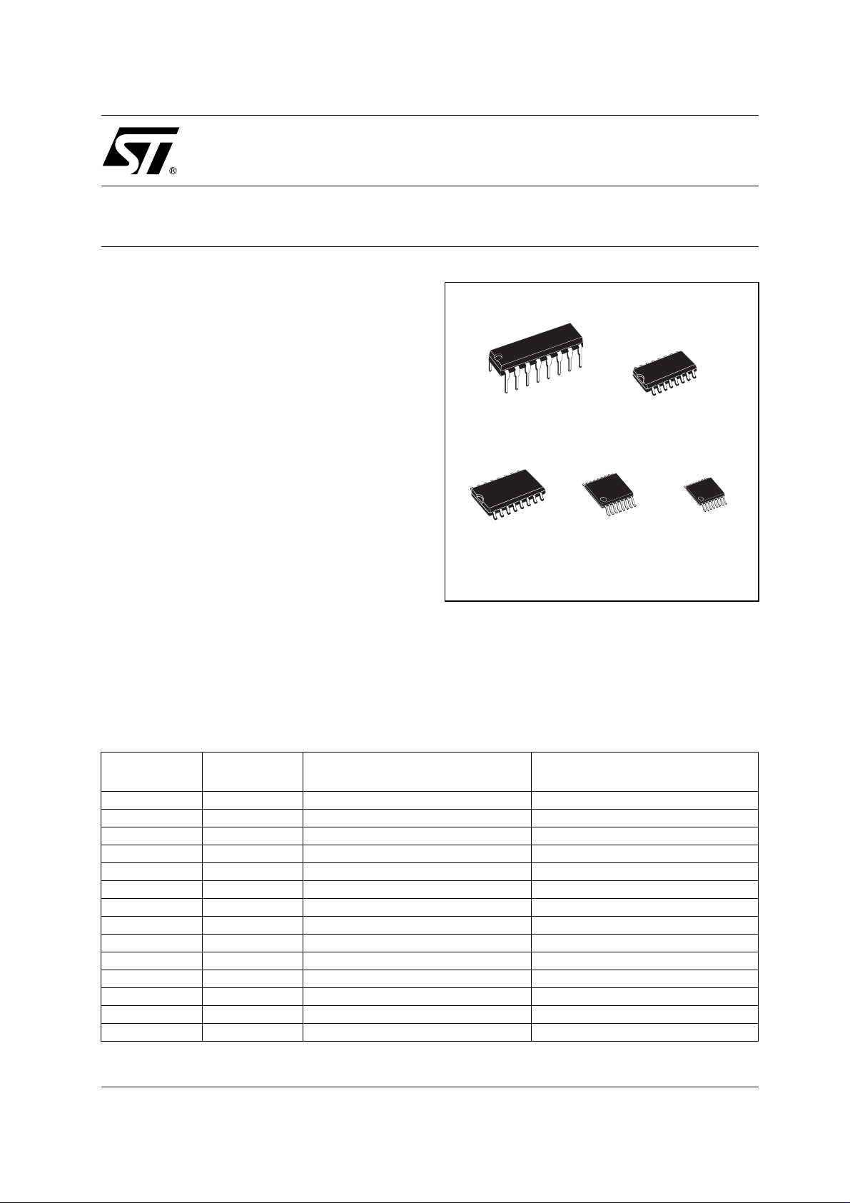
■ A VAILABLE IN DIP-16, SO-16, SO -16 LARGE
SSOP16 AND TSSOP16
DESCRIPTION
The ST3232E is a 3V powered EIA/TIA-23 2 and
V.28/V.24 communication interfaces with low
power requirements, high data-rate capabilities
and enhanced electrostatic discharge (ESD)
protection to ±8kV using IEC1000-4-2 Contact
Discharge and ±15kV using the Human Body
Model. ST3232E has a proprietary low dropout
transmitter output stage providing true RS-232
performance from 3 to 5V supplies witha a dua l
charge pump. The charge pump requires only four
small 0.1µF standard external capacitors for
operations from 3V supply.
The ST3232E has two receivers and two drivers.
DIP SOP
SOP Large
TSSOPSSOP
The device is guaranteed to run at data rates of
250Kbps while maintaining RS-232 output levels.
Typical applications are Notebook, Subnotebook
and Palmtop Computers, Battery Powered
Equipment, Hand-Held Equipment, Peripherals
and Printers.
ORDERING CODES
Type
ST3232ECN 0 to 70 °C DIP-16 25parts per tube / 40tube per box
ST3232EBN -40 to 85 °C DIP-16 25parts per tube / 40tube per box
ST3232ECD 0 to 70 °C SO-16 (Tube) 50parts per tube / 20tube per box
ST3232EBD -40 to 85 °C SO-16 (Tube) 50parts per tube / 20tube per box
ST3232ECDR 0 to 70 °C SO-16 (Tape & Reel) 2500 parts per reel
ST3232EBDR -40 to 85 °C SO-16 (Tape & Reel) 2500 parts per reel
ST3232ECW 0 to 70 °C SO-16 Large (Tube) 50parts per tube / 20tube per box
ST3232EBW -40 to 85 °C SO-16 Large (Tube) 50parts per tube / 20tube per box
ST3232ECWR 0 to 70 °C SO-16 Large (Tape & Reel) 1000 parts per reel
ST3232EBWR -40 to 85 °C SO-16 Large (Tape & Reel) 1000 parts per reel
ST3232ECPR 0 to 70 °C SSOP16 (Tape & Reel) 1350 parts per reel
ST3232EBPR -40 to 85 °C SSOP16 (Tape & Reel) 1350 parts per reel
ST3232ECTR 0 to 70 °C TSSOP16 (Tape & Reel) 2500 parts per reel
ST3232EBTR -40 to 85 °C TSSOP16 (Tape & Reel) 2500 parts per reel
Temperature
Range
Package Comments
1/16April 2003

ST3232E
PIN CONFIGURATION
PIN DESCRIPTION
PlN N° SYMBOL NAME AND FUNCTION
1
2 V+ Doubled Voltage Terminal
3
4
5
6 V- Inverted Voltage Terminal
7
8
9
10
11
12
13
14
15 GND Ground
16
C1+ Positive Terminal for the first Charge Pump Capacitor
- Negative Terminal for the first Charge Pump Capacitor
C
1
+ Positive Terminal for the second Charge Pump Capacitor
C
2
- Negative Terminal for the second Charge Pump Capacitor
C
2
T2
R2
R1
T1
R2
T2
T1
R1
V
OUT
IN
OUT
IN
IN
OUT
IN
OUT
CC
Second Transmitter Output Voltage
Second Receiver Input Voltage
Second Receiver Output Voltage
Second Transmitter Input Voltage
First Transmitter Input Voltage
First Receiver Output Voltage
First Receiver Input Voltage
First Transmitter Output Voltage
Supply Voltage
ABSOLUTE MAXIMUM RATINGS
Symbol Parameter Value Unit
V
V+
V- Inverted Voltage Terminal 0.3 to -7 V
V+ +|V-| 13 V
T
R
T
OUT
R
OUT
t
SHORT
Absolute Maximum Ratings are those values beyond which damage to the device may occur. Functional operation under these condition is
not implied. V+ and V- can have a maximum magnitude of +7V, but their absolute addition can not exceed 13 V.
2/16
Supply Voltage
CC
Doubled Voltage Terminal (V
Transmitter Input Voltage Range
IN
Receiver Input Voltage Range
IN
Transmitter Output Voltage Range
Receiver Output Voltage Range -0.3 to (VCC + 0.3)
Transmitter Output Short to GND Time
-0.3 to 6 V
- 0.3) to 7
CC
-0.3 to 6 V
± 25 V
± 13.2 V
Continuous
V
V
ST3232E
ESD PERFORMANCE: TRANSMITTER OUTPUTS, RECEIVER INPUTS
Symbol Parameter Test Conditions Min. Typ. Max. Unit
ESD ESD Protection Voltage Human Body Model ±15 kV
ESD ESD Protection Voltage IEC-1000-4-2 ±8kV
ELECTRICAL CHARACTERISTICS
(C
- C4 = 0.1µF, VCC = 3V to 5.5V, TA = -40 to 85°C, unless otherwise specified.
1
Typical values are referred to T
Symbol Parameter Test Conditions Min. Typ. Max. Unit
I
SUPPLYVCC
Power Supply Current No Load VCC = 3V or 5V TA = 25°C 0.3 1 mA
LOGIC INPUT ELECTRICAL CHARACTERISTICS
(C
- C4 = 0.1µF, VCC = 3V to 5.5V, TA = -40 to 85°C, unless otherwise specified.
1
Typical values are referred to T
Symbol Parameter Test Conditions Min. Typ. Max. Unit
Input Logic Threshold Low T-IN 0.8 V
V
TIL
V
V
Transmitter Input
HYS
Histeresys
Input Logic Threshold High VCC = 3.3V 2 V
TIH
Input Leakage Current T-IN ± 0.01 ± 1 µA
I
IL
= 25°C)
A
= 25°C)
A
= 5V 2.4
V
CC
0.25 V
TRANSMITTER ELECTRICAL CHARACTERISTICS
- C4 = 0.1µF tested at VCC = 3V to 5.5V, TA = -40 to 85°C, unless otherwise specified.
(C
1
Typical values are referred to T
Symbol Parameter Test Conditions Min. Typ. Max. Unit
V
R
I
Output Voltage Swing All Transmitter outputs are loaded with
TOUT
Transmitter Output
TOUT
Resistance
Output Short Circuit
TSC
Current
I
Output Leakage Current VCC = 0V or 3V to 5.5V V
TOL
= 25°C)
A
3KΩ to GND
VCC = V+ = V- = 0V V
Transmitters Disable
± 5 ± 5.4 V
= ± 2V 300 10M Ω
OUT
± 60 mA
OUT
= ± 12V
± 25 µA
3/16
ST3232E
RECEIVER ELECTRICAL CHARACTERISTICS
(C
- C4 = 0.1µF tested at VCC = 3V to 5.5V, TA = -40 to 85°C, unless otherwise specified.
1
Typical values are referred to T
Symbol Parameter Test Conditions Min. Typ. Max. Unit
V
V
V
V
R
V
V
Receiver Input Voltage
RIN
Operating Range
RS-232 Input Threshold
RIL
Low
RS-232 Input Threshold
RIH
High
Input Hysteresis 0.5 V
RIHYS
Input Resistance TA = 25°C 3 5 7 KΩ
RIN
TTL/CMOS Output Voltage
ROL
Low
TTL/CMOS Output Voltage
ROH
High
TIMING CHARACTERISTICS
(C
- C4 = 0.1µF, VCC = 3V to 5.5V, TA = -40 to 85°C, unless otherwise specified.
1
Typical values are referred to T
Symbol Parameter Test Conditions Min. Typ. Max. Unit
Data Transfer Rate RL = 3KΩ CL2= 1000pF
D
R
t
PHLR
t
t
t
|t
- t
|t
- t
Transmi tter Skew is measured at the transmi tter zero cross points
Propagation Delay Input to
Output
PLHR
Receiver Output Enable
OER
Time
Receiver Output Disable
ODR
Time
Transmitter Propagation
PHLT
Delay Difference
|
THL
Receiver Propagation Delay
PHLR
Difference
|
THR
Trnasition Slew Rate TA = 25°C RL = 3KΩ to 7KΩ VCC = 3.3V
S
RT
= 25°C)
A
-25 25 V
TA = 25°C VCC = 3.3V 0.6 1.1 V
= 25°C VCC = 5V 0.8 1.5
T
A
TA = 25°C VCC = 3.3V 1.4 2.4 V
= 25°C VCC = 5V 1.8 2.4
T
A
I
= 1.6mA 0.4 V
OUT
I
= -1mA VCC-0.6 VCC-0.1 V
OUT
= 25°C)
A
250 Kbps
one trasmitter switching
R
XIN
= R
XOUT
CL = 150pF 0.15 µs
Normal Operation 50 ns
Normal Operation 50 ns
(Note 1) 200 ns
50 ns
measured from +3V to -3V or -3V to +3V
CL = 150pF to 1000pF
C
= 150pF to 2500pF
L
6
4
30
30
V/µs
V/µs
4/16
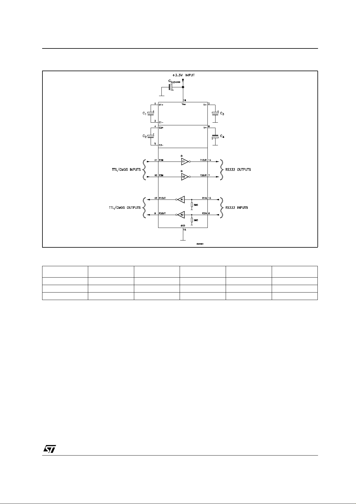
APPLICATION CIRCUITS
ST3232E
CAPACITANCE VALUE (µF)
V
CC
3.0 to 3.6 0.1 0.1 0.1 0.1 0.1
4.5 to 5.5 0.047 0.33 0.33 0.33 0.1
3.0 to 5.5 0.1 0.47 0.47 0.47 0.1
C1 C2 C3 C4 Cbypass
5/16

ST3232E
TYPICAL PERFORMANCE CHARACTERISTICS (unless otherwise specified Tj = 25°C)
Figure 1 : Output Current vs Output High Voltage
Figure 4 : Output Current vs Output Low Voltage
Figure 2 : Output Current vs Output High Voltage
Figure 3 : Output Current vs Output Low Voltage
Figure 5 : Voltage Transfer Characteristics
for Trasmitter Inputs
Figure 6 : Receiver Input Resistance
6/16

ST3232E
Plastic DIP-16 (0.25) MECHANICAL DATA
mm. inch
DIM.
MIN. TYP MAX. MIN. TYP. MAX.
a1 0.51 0.020
B 0.77 1.65 0.030 0.065
b 0.5 0.020
b1 0.25 0.010
D 20 0.787
E 8.5 0.335
e 2.54 0.100
e3 17.78 0.700
F 7.1 0.280
I 5.1 0.201
L 3.3 0.130
Z 1.27 0.050
P001C
7/16

ST3232E
SO-16 MECHANICAL DATA
DIM.
A 1.75 0.068
a1 0.1 0.2 0.004 0.008
a2 1.65 0.064
b 0.35 0.46 0.013 0.018
b1 0.19 0.25 0.007 0.010
C 0.5 0.019
c1 45˚ (typ.)
D 9.8 10 0. 385 0.393
E 5.8 6. 2 0. 228 0.244
e 1.27 0.050
e3 8.89 0.350
F 3.8 4.0 0.149 0.157
G 4.6 5.3 0.181 0.208
L 0.5 1.27 0.019 0. 050
M 0.62 0.024
S8 ˚ (max.)
MIN. TYP MAX. MIN. TYP. MAX.
mm. inch
8/16
PO13H

SO-16L MECHANICAL DATA
ST3232E
DIM.
A 2.65 0.104
a1 0.1 0.2 0.004 0.008
a2 2.45 0.096
b 0.35 0.49 0.014 0.019
b1 0.23 0.32 0.009 0.012
C 0.5 0.020
c1 45˚ (typ.)
D 10.1 10.5 0.397 0.413
E 10.0 10.65 0.393 0.419
e 1.27 0.050
e3 8.89 0.350
F 7.4 7.6 0.291 0.300
G
L 0.5 1.27 0.020 0. 050
M 0.75 0.029
S8 ˚ (max.)
MIN. TYP MAX. MIN. TYP. MAX.
mm. inch
PO13I
9/16

ST3232E
SSOP16 MECHANICAL DATA
mm. inch
DIM.
MIN. TYP MAX. MIN. TYP. MAX.
A 2 0.079
A1 0.05 0.21 0.002 0.008
A2 1.65 1.85 0.065 0.073
b 0.22 0.38 0.009 0.015
c 0.09 0.25 0.0035 0.0098
D 5.9 6.5 0.232 0.256
E 7.4 8.2 0.291 0.323
E1 5.3 5 5.6 0.197 0.209 0.220
e 0.65 0.0256
K0˚ 8˚0˚ 8˚
L 0.55 0.95 0.022 0.037
A2
A
A1
b
e
c
K
L
E
D
E1
PIN 1 IDENTIFICATION
10/16
1
7299589/A

ST3232E
TSSOP16 MECHANICAL DATA
mm. inch
DIM.
MIN. TYP MAX. MIN. TYP. MAX.
A 1.2 0.047
A1 0.05 0.15 0.002 0.004 0.006
A2 0.8 1 1.05 0.031 0.039 0.041
b 0.19 0.30 0.007 0.012
c 0.09 0.20 0.004 0.0079
D 4.9 5 5.1 0.193 0.197 0.201
E 6.2 6.4 6.6 0.244 0.252 0.260
E1 4.3 4.4 4.48 0.169 0.173 0.176
e 0.65 BSC 0.0256 BSC
K0˚ 8˚0˚ 8˚
L 0.45 0.60 0.75 0.018 0.024 0.030
A2
A
A1
b
e
c
K
L
E
D
E1
PIN 1 IDENTIFICATION
1
0080338D
11/16

ST3232E
Tape & Reel SO-16 MECHANICAL DATA
mm. inch
DIM.
MIN. TYP MAX. MIN. TYP. MAX.
A 330 12.992
C 12.8 13.2 0.504 0.519
D 20.2 0.795
N 60 2.362
T 22.4 0.882
Ao 6.45 6.65 0.254 0.262
Bo 10.3 10.5 0.406 0.414
Ko 2.1 2.3 0.082 0.090
Po 3.9 4.1 0.153 0.161
P 7.9 8.1 0.311 0.319
12/16

ST3232E
Tape & Reel SO-16L MECHANICAL DATA
mm. inch
DIM.
MIN. TYP MAX. MIN. TYP. MAX.
A 330 12.992
C 12.8 13.2 0.504 0.519
D 20.2 0.795
N 60 2.362
T 22.4 0.882
Ao 10.8 11.0 0.425 0.433
Bo 10.7 10.9 0.421 0.429
Ko 2.9 3.1 0.114 0.122
Po 3.9 4.1 0.153 0.161
P 11.9 12.1 0.468 0.476
13/16

ST3232E
Tape & Reel SSOP16 MECHANICAL DATA
mm. inch
DIM.
MIN. TYP MAX. MIN. TYP. MAX.
A 330 12.992
C 12.8 13.2 0.504 0.519
D 20.2 0.795
N 60 2.362
T 22.4 0.882
Ao 8.4 8.6 0.331 0.339
Bo 6.7 6.9 0.264 0.272
Ko 2.9 3.1 0.114 0.122
Po 3.9 4.1 0.153 0.161
P 11.9 12.1 0.468 0.476
14/16

ST3232E
Tape & Reel TSSOP16 MECHANICAL DATA
mm. inch
DIM.
MIN. TYP MAX. MIN. TYP. MAX.
A 330 12.992
C 12.8 13.2 0.504 0.519
D 20.2 0.795
N 60 2.362
T 22.4 0.882
Ao 6.7 6.9 0.264 0.272
Bo 5.3 5.5 0.209 0.217
Ko 1.6 1.8 0.063 0.071
Po 3.9 4.1 0.153 0.161
P 7.9 8.1 0.311 0.319
15/16

ST3232E
o
rmation furnished is believed to be accurate and reliable. However, STMicroelectronics assumes no responsibility for the
sequences of u se of such inform ation nor for any in fring ement of p atents or o ther ri ghts of th ird p arties which may resul t fr o m
use. No license is granted by implication or otherwise under any patent or patent rights of STMicroelectronics. Specifications
ntioned in this publication are subject to change without notice. This publication supersedes and replaces all information
viously supplied. STMicroelectronics products are not authorized for use as critical components in life support devices or
tems without express written approval of STMicroelectronics.
ustralia - Brazil - Canada - China - Finland - France - Germany - Hong Kong - India - Israel - Italy - Japan - Malaysia - Malta - Morocco
© The ST logo is a registered trademark of STMicroelectronics
© 2003 STMicroelectronics - Printed in Italy - All Rights Reserved
STMicroelectronics GROUP OF COMPANIES
Singapore - Spain - Sweden - Switzerland - United Kingdom - United States.
© http://www.st.com
16/16
 Loading...