

February 98 42 1726 00
This ispreliminary information on aproduct indevelopment orundergoing evaluation. Detailsare subject to change without notice.
ST18-AU1
SIX-CHANNEL DOLBY AC3/MPEG2 AUDIO DECODER
PRELIMINARY DATA
FEATURES
■ Single chip multi-function audio decoder able to
decompress DOLBY AC-3, MPEG-1 and
MPEG-2 audio streams.
■ Maximum 5.1 channel DOLBY AC-3 decoding
to 2 channel mixed down output with DOLBY
surround compatible or karaoke capable option.
■ Variable bit rate MPEG-1 layer II audio
decoding, and MPEG-2 multi-channel audio
decoding for karaoke capable application.
■ Input data rates
■ up to 448 Kbits/s for AC-3 decoder
■ up to 912 Kbits/s for MPEG-1 or MPEG-2
audio decoder
■ Supports up to 8 channel DVDlinear PCMinput
at max rate of 6.144 Mbits/s down-mixing and/
or sub-sampling to 2 to 6 channels.
■ Accepts MPEG-1 or DVD/MPEG-2 PES input
packets.
■ Programmable D950 core
■ System time clock provides A/V
synchronization and PTS packet extraction.
■ Automatic error concealment on CRC or
synchronization error.
■ 6 channel PCM audio output at 16/18/20/24 bit.
Sampling rate of 32/44.1/48/96 kHz.
■ Two on-chip PLLs providing full circuit operation
with only one external 27 MHz clock.
■ I
2
C interface for host control
■ Multi-format i
2
S serial data input port and
decoded audio PCM output port.
■ IEC-958 (S/PDIF) formatter and transmitter for
DOLBY AC-3, MPEG audiobit stream, oraudio
PCM.
■ Dedicated hardware for emulation and test,
IEEE 1149.1 (JTAG).
■ 3.3V power supply, I/O’s 5V tolerant, 0.35µM
HCMOS6 technology.
■ 160 pin PQFP package
APPLICATIONS
■ Digital video disc (DVD) player
■ Digital TV (DBS/DVB) receiver
■ PC multimedia
■ Consumer digital audio
Interrupt
controller
Clocks and
timers
I2C Host
interface
2
Input serial
interface
IEC-958
(S/PDIF)
output
16K Program
memory
3
Output serial
interface
D950
DSP
core
24K Data
memory
DMA
controller
Emulation
unit and TAP
Bus switch
unit

2/87
Table of Contents
4
1 INTRODUCTION......................................................5
2 PINDESCRIPTIONS................................................... 7
3 FUNCTIONALOVERVIEW .............................................12
4 HOSTINTERFACE ...................................................16
4.1 HOSTINTERFACEREGISTERS ...................................16
4.2 LISTOFHOSTCOMMANDS ......................................19
5 INPUTSERIALINTERFACE............................................25
5.1 INPUT SERIAL INTERFACE REGISTERS . . . . . . . . . . . . . . . . . . . . . . . . . . . . 25
5.2 INPUT FIFO . . . . . . . . . . . . . . . . . . . . . . . . . . . . . .......................27
5.2.1 Input FIFO registers . . . . . . . . . . . . . . . . . . . .....................27
6 INPUTANDOUTPUTBUFFERS ........................................ 29
6.1 INPUTBUFFER.................................................29
6.2 OUTPUTBUFFER ...............................................29
6.2.1 Input and output buffer registers . . . . ..........................29
7 OUTPUTSERIALINTERFACE-PCMOUTPUT ............................31
7.1 OUTPUTSERIALINTERFACEREGISTERS ..........................31
8 INTERRUPT CONTROLLER . . . . . . . . . . . . . . . . . . . ........................34
8.1 INTERRUPT CONTROLLER REGISTERS . . . . . . . . ....................35
9 DMACONTROLLER..................................................40
9.1 DMAOPERATION ...............................................40
9.2 DMAREGISTERS ...............................................41
9.2.1 Address registers . . . . . . . . . . . . . . . . . . ........................41
9.2.2 Counting registers . . ....................................... 41
9.2.3 Control registers . .......................................... 42
10 IEC-958 TRANSMITTER . . . . . . . . ....................................... 44
10.1 IEC-958 TRANSMITTER REGISTERS . . . . . . . . . . . . . . . . . . . . . ..........44
11 MEMORY ..........................................................46
11.1 INTERNALMEMORYRESOURCE..................................46
11.2 I-MEMORY BUS EXTENSION - DIRECT AND THROUGH BSU . . . . . . . . . . . 47
11.3 X-MEMORY BUS EXTENSION - DIRECT AND THROUGH BSU ...........47
11.4 Y-MEMORY BUS EXTENSION THROUGH BSU . . . . . . . . . . .............47
12 BUSSWITCHUNIT...................................................48
12.1 BSUCONTROLREGISTERS ...................................... 48
13 CLOCKS AND TIMERS UNIT . . . . . . . . . . .................................51
13.1 OPERATION ................................................... 51
1

3/87
Table of Contents
13.1.1 Audio clock prescaler . . . ....................................51
13.2 CLOCKS AND TIMERS REGISTERS . . . .............................52
14 JTAGIEEE1149.1TESTACCESSPORT.................................55
15 EMULATIONUNIT ...................................................56
16 D950CORE .........................................................58
16.1 D950COREREGISTERS..........................................60
17 YSPACEMEMORYMAPPING .........................................61
17.1 MEMORYMAP .................................................61
17.2 CLOCKS AND TIMERS REGISTERS . . . .............................62
17.3 IEC-958 TRANSMITTER (S/PDIF OUTPUT) REGISTERS . . . .............63
17.4 PCMREGISTERS ............................................... 63
17.5 INPUT/OUTPUT BUFFER REGISTERS . . . . . . . . . . . . . . . . . . . . . . . . . . . . . . 63
17.6 SERIALINPUT1REGISTERS .....................................64
17.7 SERIALINPUT0REGISTERS .....................................64
17.8 HOSTINTERFACEREGISTERS ...................................64
17.9 BUSSWITCHUNITREGISTERS ...................................64
17.10PLLREGISTERS ................................................ 65
17.11DMACONTROLLERREGISTERS ..................................65
17.12 INTERRUPT CONTROLLER REGISTERS ............................66
17.13D950CORECONTROLREGISTERS................................66
17.14 DATA AND PROGRAM MEMORY MAPPING . . . . . . . . . . . . . . . . ..........67
18 ELECTRICAL SPECIFICATIONS . . . . . . . . . . . . . . . . . . . . . . . . . . . .............68
18.1 DCABSOLUTEMAXIMUMRATINGS................................68
18.2 DC ELECTRICAL CHARACTERISTICS . . . . . . . . . . . . . . . . . . . . . . . . . . . . . . 68
18.3 ACCHARACTERISTICS .......................................... 69
18.3.1 Clocks electrical characteristics . . .............................72
18.3.2 E-bus (I direct extension) . . . . . . . . . . . . . . . . . . . . . . . . . . . . . . . . . . . . 73
18.3.3 E-bus (X direct extension) . . . . . . . . . . . . . . . ....................74
18.3.4 E-bus (I BSU) . . . . . . . . . . . . . . . . . . . . . . . . . . . . . . . . ............. 75
18.3.5 E-bus (X BSU) . . ..........................................76
18.3.6 E-bus (Y BSU) . . ..........................................77
18.3.7 D950 control . . . . . . . . . . . . . .................................78
18.3.8 I2C Host interface . . . . . ....................................79
18.3.9 PCM and SPDIF .......................................... 80

4/87
Table of Contents
4
18.3.10I2S Data Input 0 . ..........................................81
18.3.11I2S Data Input 1 . ..........................................82
19 ST18-AU1 PACKAGE SPECIFICATIONS . . . . . . . . . . .......................83
19.1 ST18-AU1 PACKAGE PINOUT . ....................................83
19.2 160PINPQFPPACKAGEDIMENSIONS .............................84
20 DEVICEID..........................................................86
21 ORDERING INFORMATION . . . . . . . . . . . . . . . . . ...........................86

5/87
ST18-AU1
1 INTRODUCTION
The ST18-AU1 is a single-chip multi-function audio processor for Dolby AC-3, MPEG-1/
MPEG-2 Layer-I/II audio encoded bitstreams, and DVD Linear PCM. It is capable of decoding
up to 5.1 channels of input Dolby AC-3 or MPEG-2 multi-channel encoded audio, and down
mixing to 2 channels of PCM output audio. Maximum input data rates for Dolby AC-3 bitstream
and MPEG-2 audio bitstream are 448 Kbits/s and 912 Kbits/s respectively. It also supports up
to 8 channel linear PCM input with by-pass, down-sampling, and down-mixing function. The
linear PCM multi-channel input modes available are:
• 48 kHz/16-bit up to 8 ch @ max 6.144 Mbps
• 48 kHz/20-bit up to 6ch @ max 5.760 Mbps
• 48 kHz/24-bit up to 5ch @ max 5.760 Mbps
• 96 kHz/16-bit up to 4ch @ max 6.144 Mbps
• 96 kHz/20-bit up to 3ch @ max 5.760 Mbps
• 96 kHz/24-bit up to 2ch @ max 4.608 Mbps
• 44.1 kHz/16-bit 2ch (CD-DA).
The input bitstream is taken from the multi-format serial input, and decoded according to the
selected MPEG-1, MPEG-2 (in the case of Karaoke capable mode), AC-3 decoder or Linear
PCM processor. A Packet Demux de-multiplexes the input if it is MPEG-1 or DVD/MPEG-2
PES packetized. For an input bitstream with more than 2 encoded audio channels, the
decoded channels are mixed down to 2 channels with the Dolby Surround compatible or
karaoke capable option, and outputted through a multi-format serial output port. The input AC3, MPEG bitstream, or decoded PCM can be outputted through an IEC-958 (S/PDIF)
Formatter/Transmitter. The AC-3 or MPEG S/PDIF output bitstream is delayed and
synchronized with the output decoded PCM.
The Karaoke Capable mode defined in Dolby AC-3 or DVD to allow the multi-channel audio
stream to convey channels designed as L, R (2-ch stereo music), M (guide melody), and V1,
V2 (one or two vocal/supplementary tracks) are supported. This Karaoke capable decoder
allows the user to choose to have the decoder reproduce any of the guide melody and vocal/
supplementary channels. Centre and surround mix levels either controlled by the user or within
the bitstream are used to down mix the M channel and the V1, V2 channels respectively.
The selectable Linear PCM Processor functions are:
• down-mixing to 2 channels,
• down-sampling for 96kHz to 48kHz,
• noise shaped quantization for 24-bits or 20-bits to 16-bits.
Depending on the application, the decoded PCM audio output is selectable to be 16, 18, 20 or
24 bits, and the sampling rates of the PCM output are 32 kHz, 44.1 kHz, 48 kHz or 96 kHz.
External A/V synchronization can be assisted by the System Time Clock (STC) within the
Timer and the PTS extracted from the packetized input. A serial I
2
C interface to host
2
6/87
ST18-AU1
microcontroller is provided to allow ST18-AU1 operation control, bitstream information and
internal status access.
A typical DVD back-end system configuration is shown in Figure 1.1.
Figure 1.1 Typical DVD back-end system configuration
Video bitstream
Control
DRAM
MPEG-2 video
decoder
27 MHz osc
Video
encoder
ST18-AU1
audio
processor
Audio DAC
System layer
controller
Audio bitstream
Control
I2C
I2S
Compressed
system input
bitstreams
Video
output
L/Lt
R/Rt
IEC-958
(S/PDIF)
AC-3/MPEG

7/87
ST18-AU1
2 PIN DESCRIPTIONS
The following tables detail the ST18-AU1 pin set. There is one table for each group of pins.
The tables detail the pin name, type and a short description of the pin function.
Signal names have a bar above if they are active low, otherwise they are active high.
Table 2.1 Direct I bus extension (35 pins)
Pin name Type Description
IDE0-15 I/O Instruction data extension bus.
IAE0-15 O Instruction address extension bus.
IRDE O I-extension bus read strobe.Active low.
IWRE O I-extension bus write strobe. Active low.
IBSE O I-extension bus strobe. Active low. Asserted at the beginning of I-bus read/
write cycle.
8/87
ST18-AU1
Table 2.2 Direct X bus extension / Bus extension through bus switch unit (39 pins)
Table 2.3 General purpose parallel port (8 pins)
Pin name Type Description
ED0-15 I/O Bus switch unit (BSU) X/Y/I data extension bus.
EA0-15 O BSU X/Y/I address extension bus.
EIRD O BSU I-extension bus read strobe EIRD output.
EIWR O BSU I-extension bus writestrobe EIWR output.
XBSE O X_extension bus data strobe (BSU not used).
EYRD O BSU Y-extension bus read strobe EYRD output.
EYWR O BSU Y-extension bus write strobe EYWR output.
XRDE_EXRD O Multiplexed output.
In direct X-bus extension mode (BSU not used):
X-extension bus read strobe (XRDE). Active low when reading from external X-memory.
In X extension through BSU mode:
BSU X-extension bus read strobe (EXRD). Active low when reading from
external memory (when bit I/Mof XER register is ‘1’: Intel mode).
BSU extensionbus data strobe (EDS). Activelow when reading fromorwriting to external memory (when bit I/M of XER register is ‘0’ Motorola mode).
XWRE_EXWR O Multiplexed output.
In direct X-bus extension mode (BSU not used):
X-extension bus write strobe (XWRE). Active low when writing to external
X-memory.
In X extension through BSU mode:
BSU X-extension bus write strobe (EXWR). Active low when writing to external memory (when bit I/M of XER register is ‘1’: Intel mode).
Extension bus read /write signal (ERD_WR). Low during write cycle, otherwise high (when bit I/M of XER register is ‘0’: Motorola mode).
Pin name Type Description
P0-7 I/O Parallel port I/O. Each pin can be programmed as input or output.
On reset, all pins are inputs.

9/87
ST18-AU1
Table 2.4 Clocks (13 pins)
Table 2.5 I
2
C Host interface (3 pins)
Pin name Type Description
EXTAL0 I Oscillator0 input. DSP PLL.
XTAL0 O Oscillator0 output. Nominal oscillator frequency is 27 MHz.
EXTAL1 I Oscillator1 input. Audio PLL
XTAL1 O Oscillator1 output. Nominal oscillator frequency is 27 MHz.
CLK0 I Direct clock input for D950 core.
CLK0_MODE I Clock0 mode select input.
When low, select output of DSP PLL for DSP Clock In
When high, select CLK0 (bypass DSP PLL) for DSP Clock In
CLK1 I Direct audio clock input.
CLK1_MODE I Clock1 mode select input.
When low, select output of audio PLL for audio clock
When high, select CLK1 (bypass audio PLL) for DSP Clock In
PLL_MODE I PLL mode select input
When low, select oscillator 1 for audio PLL
When high, select oscillator 0 for audio PLL
CLKOUT O Output clock (at input clock/2 frequency).
INCYCLE O Instruction cycle.
Asserted high for 1 CLKOUT cycle at the beginning of instruction cycle.
SCLK I/O External audio clock/audio clock prescaler output
MCLK_MODE I SCLK mode select input
When low,SCLK = output (internal audio master clock from clock prescaler)
When high, SCLK = input (external audio master clock)
Pin name Type Description
HDA I/O I2C Data input/output (open drain output).
HCL /O I2C Clock input/output (open drain output).
HSAS I Slave address select
10/87
ST18-AU1
Table 2.6 Data input 0 (4 pins)
Table 2.7 Data input 1 (3 pins)
Table 2.8 PCM output (5 pins)
Table 2.9 IEC-958 transmitter (SPDIF) output (1 pin)
Table 2.10 Interrupt controller interface (1 pin)
Pin name Type Description
DIN0 I Serial data input
CLKDIN0 I/O Data input clock
Input in slave mode, output in master mode.
WSDIN0 I/O Data input word select
Input in slave mode, output in master mode.
DREQ0 O Request for data input. Active low.
Pin name Type Description
DIN1 I Serial data input
CLKDIN1 I Data input clock
Input in slave mode, output in master mode.
WSDIN1 O Data input word select
Input in slave mode, output in master mode.
Pin name Type Description
PCM_OUT0 O PCM data output 0
PCM_OUT1 O PCM data output 1
PCM_OUT2 O PCM data output 2
SCLKPCM O PCM output clock (common)
WSPCM O PCM output word select (common)
Pin name Type Description
SPDIFOUT O S/PDIF signal
Pin name Type Description
IRQ I Interrupt request. Active low.
Maskable, programmable as falling edge or low level triggered (default is
level triggered).

11/87
ST18-AU1
Table 2.11 D950-Core control (3 pins)
Table 2.12 Emulation unit (4 pins)
Table 2.13 JTAG IEEE 1149.1 test access port(5 pins)
Pin name Type Description
RESET I Reset input. Active low.
Initializes the 950-Core to the Reset state.
LP I Low power input. Active low.
MODE_RESET I Mode selection for Reset.
When low, forces reset address to 0x0000.
When high, forces reset address to 0xFC00.
Pin name Type Description
ERQ I Emulator halt request. Active low.
Halts program execution and enters emulation mode.
IDLE O Output flag asserted high whenthe processor is halted due to an emulation
halt request or a valid breakpoint condition.Asserted low when the proces-
sor is not Halted or during execution of an instruction under control of the
emulator.
HALTACK O Halt acknowledge. Active high.
Asserted high when the processor is halted from an Emulator Halt request
or when a valid Breakpoint condition is met.
SNAP O Snapshot. Active high.
Asserted high when executing an instruction if Snapshot mode is enabled.
Pin name Type Description
TDI I Test data input.
TCK I Test clock.
TMS I Test mode select.
TDO O Test data output.
TRST I Test logic reset (also used for Emulator module). Active low.

12/87
ST18-AU1
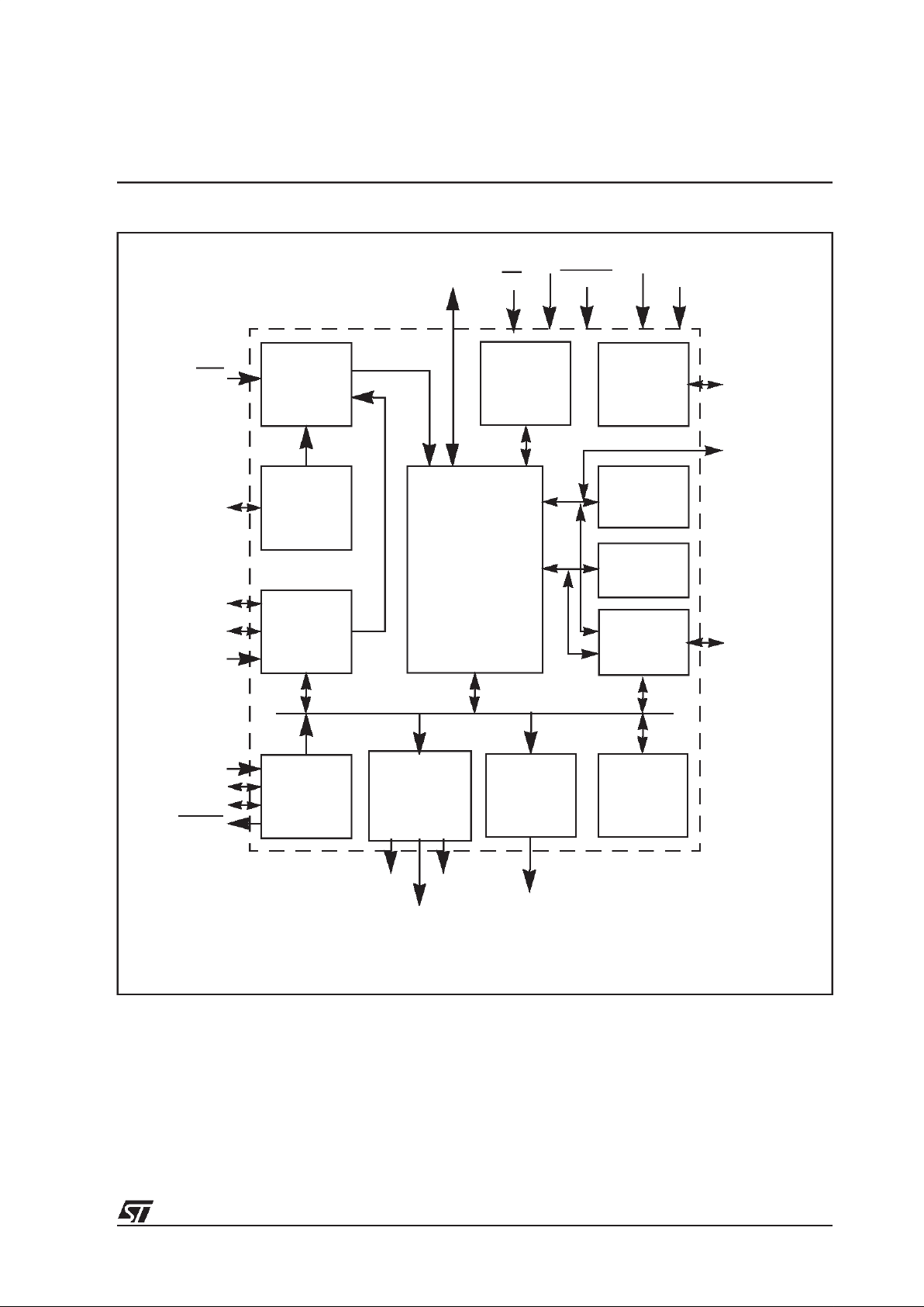
3 FUNCTIONAL OVERVIEW
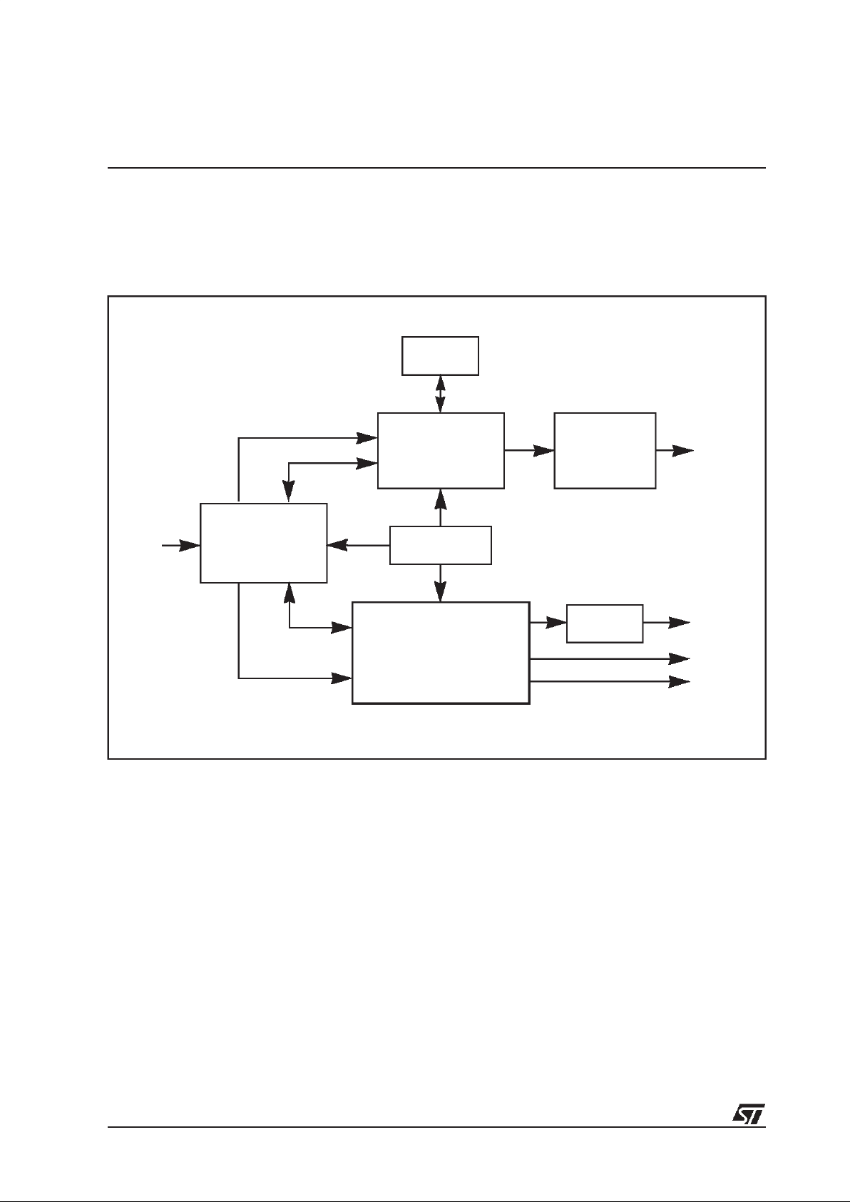
A functional block diagram of the ST18-AU1 is shown in Figure 3.1. The modules that
comprise the ST18-AU1 are outlined below and more detailed information is given in the
following chapters of this datasheet. The interconnection of these blocks and all external
interfaces are shown in the block diagram in Figure 3.2.
Figure 3.1 Functional block diagram
Timer
Host
interface
Serial
Packet
demux
interface
Linear PCM
MPEG2
decoder
Dolby AC-3
decoder
processor
Down mix
(surround)
(or Karaoke
modes)
Serial
S/PDIF
formatter
output
System
manager
Delay
Clock
inputs
Commands
status
Data
input
2 to 6 channel
PCM output
S/PDIF
output
(AC-3/MPEG
or 2 ch PCM)
13/87
ST18-AU1
Figure 3.2 ST18-AU1 block diagram
Host interface
The I
2
C serial bus interface operated in slave mode enables connection to an external host
processor. It receives operating commands, and returns host requested bitstream information
and internal status.
Interrupt
controller
Clocks and
timers
Host
interface
2
TAP
16K Program
memory
16K X-data
8K Y-data
memory
IEC-958
DMA
controller
D950
DSP
core
ST18-AU1
P0-7
RESET
VCC
GND
Clocks
HCL
HDA
HSAS
(I2C host interface)
DIN
WSDIN
CLKDIN
DREQ
SPDIFOUT
(AC-3/MPEG or PCM)
IEEE 1149.1
JTAG interface
PCM_OUT
SCLKPCM
WSPCM
I-bus
X-bus
Y-bus
IT
9
Bus switch
unit
Direct X / bus
Input serial
interfaces
memory
IRQ
(S/PDIF)
output
3
Output serial
interfaces
switch
(39 pins)
(13 pins)
MODE_RESET
LP
Direct I bus
(35 pins)

14/87
ST18-AU1
Input serial interface
The ST18-AU1 has two input serial interfaces. The interfaces are multi-format serial interfaces
for inputting audio bitstreams. Supported formats include delayed (I
2
S)/non-delayed, left/right
justified, 16/18/20/24-bit word, polarity options in L/R clock and input clock, and master/slave
mode. They provide the serial to parallel conversion and transfer the input data to the input
buffer for further processing.
Output serial interface
The ST18-AU1 has three output serial interfaces. The output serial interfaces organize the
PCM audio output into the required I
2
S serial format and generate allthe DAC control signals.
IEC-958 transmitter
The IEC-958 transmitter accepts either the AC-3/MPEG bitstream or the decoded audio output
PCM data, and formats the input in accordance with the IEC-958 (S/PDIF) specification for
output.
Interrupt controller (ITC)
The interrupt controller (ITC) manages the interrupts from the clocks and timers unit, the host
interface, and the external interrupt for the DSP core. The interrupt can be activated and
programmed as edge or level triggered.
DMA controller (DMAC)
The DMA controller (DMAC) controls data transfer between data input/output and internal data
buffers.
D950 DSP Core
The D950-Core is a general purpose programmable 16-bit fixed point Digital Signal Processor
Core. The main blocks of the D950-Core include an arithmetic data calculation unit, aprogram
control unit and an address calculation unit, able to manage up to 64k (program) and 128k
(data) x 16-bitmemory spaces.
The DSP core processes all host commands, performs input bitstream parsing,
decompression, sample down-mixing and/or subsampling, as well as input and output control.
Memory
There is 8 Kword Y-data memory on Y space, 16 Kword X-data memory on X space and 16
Kword instruction memory on I space.
Memory can be extended off-chip in one of three ways:
• Direct I-bus extension.
• Direct X-bus extension.
• I, X and Y -bus extension through the bus switch unit.

15/87
ST18-AU1
Bus switch unit
The bus switch unit (BSU) is a bi-directional switcher. It switches the 3 internal buses (I, X and
Y) to the external (E) bus.
Clocks and timers unit
The clocks and timers unit provides all the necessary clocks and timer controls for DSP
processing, and all input/output operations. In addition, a 90 kHz System Time Clock (STC) is
provided to assist audio/video synchronization in systems which include a video decoder.
Emulation unit and JTAG IEEE 1149.1 test access port
The emulation unit (EMU) performs functions dedicated to emulation and test through the
external IEEE 1149.1 JTAG interface.

16/87
ST18-AU1
4 HOST INTERFACE
The host interface is a fast I2C serial bus interface operated in slave mode. It provides
connection to an external host processor. It receives operating commands, and returns host
requested bitstream information and internal status.
4.1 Host interface registers
HSER: Host serial shift register
This 16-bit shift register is used for serial data input and output. Data is shifted MSB first. It is
not visible from the D950.
HDR: Host data register
This register is used for transfers between the HSER register and the D950.
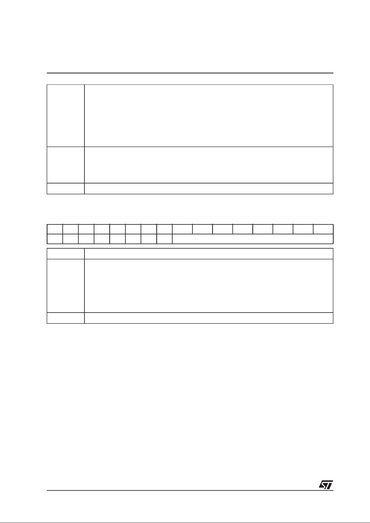
Figure 4.1 Host interface data exchange, receive mode
msb654321lsb
HCL
HDA
ack
byte 0
msb654321lsb
byte 1 .....
YD
HDR
(16-bit words)
HDA
byte 0 byte 1
msb lsb
16-bit
16-bit
msb lsb
YD
8-bit
(msb)
8-bit
(lsb)
‘0’
byte 0
8-bit
(msb) (lsb)
HDR
(8-bit words)
HDA
HSER HSER

17/87
ST18-AU1
Figure 4.2 Host interface data exchange, send mode
HCR: Host control register
All bits are cleared on reset.
15 14 13 12 11 10 9 8 7 6 5 4 3 2 1 0
- - - BERRIEN
ACKFIEN
STOPI-EN- HTIEN - - - - - ACK-
OFF
WS HEN
Bit Function
HEN Host interface enable
0 host interface disabled
1 host interface enabled
WS Word size
0 8-bit word
1 16-bit word
ACKOFF Acknowledge generation disable
0 acknowledge enabled
1 acknowledge disabled
msb654321lsb
HCL
HDA ack
byte 0
msb654321lsb
byte 1 .....
YD
HDR
(16-bit words)
HDA
byte 0 byte 1
msb lsb
16-bit
16-bit
msb lsb
YD
8-bit
(msb)
byte 0
8-bit
(msb) (lsb)
HDR
(8-bit words)
HDA
HSER HSER
18/87
ST18-AU1
HSR: Host status register
All bits are reset when the register is read. The register can only be read by the D950.
HTIEN Transfer interrupt enable
0 transfer interrupt disabled
1 transfer interrupt enabled
STOPIEN Stop interrupt enable
0 stop interrupt disabled
1 stop interrupt enabled
ACKFIEN Acknowledge fail interrupt
0 acknowledge fail interrupt disabled
1 acknowledge fail interrupt enabled
BERRIEN Bus error interrupt
0 bus error interrupt disabled
1 bus error interrupt enabled
- RESERVED, read as 0.
15141312 11 10 9 8 765432 1 0
- - - BERR ACK-
FAIL
STOP HDRRRQHDRWRQ------DAT-
ADIR
BUSY
Bit Function
BUSY Set whenValid slave address detected, until Stopevent or Restart event with invalid slave
address.
DATADIR Data direction (valid when Busy bit is set).
0 receive data from host
1’ send data tohost
HDRWRQ HDR write request. Set when data is required by the host. Data needs to be written into
the HDR register, this is reset whenthe HSR register is read.
HDRRRQ Host read request. Set when data has been sent by the host. Data needs to be read from
the HDR register, this is reset whenthe HSR register is read.
STOP Stop. Set when a stop condition is detected.
ACKFAIL Acknowledge fail. Set when the host does not generate an acknowledge after one data
byte has been sent.
BERR Bus error.Set when a misplaced start or stop condition is detected during transmission.
- RESERVED, read as 0.

19/87
ST18-AU1
HSAR: Host slave address register
(Default value for slave address on reset: HSAS (7...2) = 101000).
4.2 List of host commands
A list of host commands is given below.
15 14 13 12 11 10 9 8 76543210
HSA7 HSA6 HSA5 HSA4 HSA3 HSA2 HSA1 HSA0 --------
Bit Function
HSA0 Data direction (read only, written from HSER when Slave address is send by the host.
HSA1 Slave address bit 1 (read only, value of pin HSAS)
HSA2 Slave address bit 2
HSA3 Slave address bit 3
HSA4 Slave address bit 4
HSA5 Slave address bit 5
HSA6 Slave address bit 6
HSA7 Slave address bit 7
- RESERVED, read as 0.

20/87
ST18-AU1
Table 4.1 Write commands
Mnemonic Opcode
Size
(bits)
Command description and Parameter values
HostInputMode 00 8 Input mode (type of bitstream).
AC3 (default) 00
MPEG -1 01
MPEG-2 02
MPEG-2 with extension 03
PCM by pass 04
Linear PCM 05
HostInputStrmFormat 01 8 Input Stream Format
ES (Default) 00
DVD/PES 01
HostOpmode 02 8 Operating Mode
Idle (no decoding) (default) 00
Start (starts selected decoder) 01
Stop and flush (stops decoder and flush buffers) 02
Reset 03
SelfTest 04
HostMute 03 8 Mute
Off (default) 00
On 01
HostAudiStrmIdSel 04 8 Audio stream ID select
ID = 0(default) to 7 (e.g. language selection)00 - 07
HostOutputChanConf 05 8 Output channel configuration.
2/0 Lt/Rt, Dolby surround compatible X0
1/0 C X1
2/0 L/R (default) X2
3/0 LCR X3
2/1 LRl X4
3/1 LCRl X5
2/2 LRlr X6
3/2 LCRlr X7
Karaoke capable no vocal 0X
Karaoke capable vocal 1 1X
Karaoke capable vocal 2 2X
Karaoke capable vocal 1& 2 (default Karaoke) 3X
where X = do not care
HostDualMonoReproMode 06 8 Dual mono reproduction mode
Stereo (default) 00
Left mono 01
Right mono 02
Mixed mono 03

21/87
ST18-AU1
HostDynRngeCompMode 07 8 Dynamic Range Compression Mode
Line-out Mode 00
Custom Mode, Analog Dialnorm 01
Custom Mode, Digital Dialnorm (default) 02
RF Demod Mode 03
HostDynRngeCutScaleFac 08 16 Dynamic Range Compression Cut Scale Factor
0 to 0x7FFF (at ‘0’ the compression is minimum, at
0x7fff the compression is maximum).
(default: 0x 7fff)
HostDynRngeBstScaleFac 09 16 Dynamic Range Compression Boost Scale Factor
0 to 7FFF (at ‘0’ the boost is minimum, at 0x7fff the
boost is maximum).
(default: 0x7fff)
HostPcmScaleFac 0A 16 PCM Scale Factor
0 to 7FFF (default)
HostOutLfeOn 0B 8 Output LFE Present
Off (default) 00
On 01
HostSpdifOutStrmFormat 0C 8 SPDIF OutputStream Format
(the SPDIF output can send either the PCM decoded
output, or the input encoded elementary stream)
AC3/MPEG (default) 00
PCM 01
HostSpdifOutputLatency 0D 16 SPDIF Output Latency
Delay between the decoder and the bitstream sent via
the SPDIF output. The delay is expressed in multiples
of 1/Fs, where Fs is the samplefrequency. The delay is
signed.
0xffff to 0x7ffff (default: 0)
HostSpdifSmpteFrmRatCod
0E 16 SPDIF SMPTEFrame Rate Code
not indicated 00
24/1001 01
24 02
25 03
30/1001 (default) 04
30 05
50 06
60/1001 07
60 08
Table 4.1 Write commands
Mnemonic Opcode
Size
(bits)
Command description and Parameter values
22/87
ST18-AU1
HostLpcmMixAlpha0-7
HostLpcmMixBeta0-7
0F-16
17-1E
16 Linear PCM Downmixing Coefficients
In LPCM mode: Alphai isthe coefficient to downmix the
channel i into the Left channel. Betai isthe downmixing
coefficient for channel i into the Right channel.
In Ac-3 Karaoke mode: the Alpha0 to Alpha5 are used
to downmix respectively the Left, Melody, Right,
Vocal1, Vocal2 channels.Beta0 to Beta5is respectively used todownmix into the Right channel.
Alpha0 to Alpha7, Beta0 to Beta7.
HostErrorConcealMod 1F 8 Error Concealment Mode
Mute (default) 00
Disabled 01
Skip 02
HostLowPower 20 8 Low Power Stand-by Mode
Off (default) 00
On 01
HostSerialInputCtrl 21 Serial Input Control
Defines the input format.
default: I2S slave
HostSerialInoutDiv 22 Serial Input Clock Division
In master mode define the clock rate of the input.)
HostSerialOutputCtrl 23 Serial Output Control
Defines the output format.
default: I2s master
HostSerialOutputDiv 24 16 Serial Output Clock Division
In master mode define the clock rate of the output.
default: set for 44.1 Hz
HostAudioClockSel 25 Audio Clock Selection
All clocks derived from the 27MHz (default) 11
HostSamplFreq 26 16 Audio Sample Frequency (Hz)
3200 10
44100 (default) 00
48000 01
HostPcmNbBits 27 16 Number of bits per sample
16 (default) 16
18 18
20 20
WriteStc 80 32 System Time Clock
Table 4.1 Write commands
Mnemonic Opcode
Size
(bits)
Command description and Parameter values
23/87
ST18-AU1
Table 4.2 Read commands
Mnemonic Opcode
Size
(bits)
Command description and parameter value
HostVersion 40 16 Version number
HostI2cStatus 41 8 I2cStatus
No error 00
Error 01
HostInputStatus 42 8 InputStatus
No error 00
Overflow 01
Underflow 02
HostOutputStatus 43 8 OutputStatus
No error 00
Underflow 01
Overflow 02
Error decoder 04
HostSPDIFStatus 44 8 SPDIF Status
No error 00
Error 01
HostOpMode 45 8 OutputMode
(Refer to output channel configuration)
HostAudDecodErrorStatus 46 16 Audio Decoder Error Status
No error 0
Sync word 1
Sample frequency 2
Frame size 3
Number of channels 4
Decoder errors 5…f
Crc 10
HostInputSamplFreq 47 8 Input Sampling Frequency
Sampling frequency specified by the bitstream.
For AC-3 fscod is returned.
HostInputDatRate 48 8 Input Data Rate
Data rate specified by the bitstream.
For AC-3 frmsizecod is returned.
HostInputMultiChanMode 49 8 InputMultiChannelMode
For AC-3 acmod is returned.
HostKaraokCapBitstrm 4A 8 Karaoke Bitstream
Non Karaoke 00
Karaoke 01

24/87
ST18-AU1
HostLfePresent 4B 8 Lfe Present
Lfe not present 00
Lfe present 01
HodtCopyProtect 4C 8 Copy Protected
Not protected 00
Protected 01
HostOpModeOut 4D 8 Operating Mode
Idle 00
Synchronising 01
Decoding 02
HostInputBitstrmStatus 4E 8 Input Bitstream Status
Idle 00
Searching for PES sync word 01
Searching for audio frame syncword 04
STC 81 32 System Time Clock
PTS 82 32 Presentation Time Stamp
Table 4.2 Read commands
Mnemonic Opcode
Size
(bits)
Command description and parameter value

25/87
ST18-AU1
5 INPUT SERIAL INTERFACE
The ST18-AU1 has two input serial interfaces (DIN0 and DIN1). The interfaces are multiformat serial interfaces for inputting audio bitstreams. Supported formats include delayed
(I
2
S)/non-delayed, left/right justified, 16/18/20/24-bit word, polarity options in L/R clock and
input clock, and master/slave mode. They provide the serial to parallel conversion and transfer
the input data to the input buffer for further processing.
Data input interface 0 (DIN0) operates with an input FIFO which regulates the input data flow
transferred to the input buffer. Data input interface 1 (DIN1) operates in a similar way to DIN0
but it does not have an associated input FIFO.
5.1 Input serial interface registers
Each input serial interface has the following set of registers.
DIN0-1CR: Data in control register
On reset, all bits are cleared.
1514131211109876543210
--------Master
Justi-
fied
De-
layed
WS_polCLK_
pol
WS DIN-
EN
Bit Function
DINEN Input interface enable
0 input interface disabled
1’ input interface enabled
WS Input word size
Bit1 Bit 0 Input word size
0 0 16 bit
0 1 18 bit
1 0 20 bit
1 1 24 bit
CLK_pol Clock polarity
0 data and WS change on Clk falling edge
1 data and WS change on Clk rising edge
WS_pol Word size polarity
0 Left data word = WS low, Right data word = WS high
1 Left data word = WS high, Right data word = WS low
Delayed Delay inserted before first bit of data following transition of WS.
0 first bit of data occurs on transition of WS
1 first bit of data occurs with 1 Clk cycle delay relative to transition of
WS (I2S compatible).
26/87
ST18-AU1
DIN0-1DIV: Data in division register
On reset, DIN0DIV value is set to 0.
DIN1DR: Data in output register
This 16-bit register contains the serial interface input data and is read by the D950.
Justified If number of Clk cycles between WS transitions is >n(= word size)
0 start justified:nbits read, starting from first bit:
just after WS transition if Delayed =’0’
with 1 clk cycle delay after WS transition if Delayed=’1’
1 end justified, end bit beein last bit received:
just before WS transition if Delayed =’0’
just after WS transition if Delayed =’1’
Master Master or slave operation
0 slave
1 master
NOTE: this bit must be defined before the input interface enable (DINEN) bit is set.
- RESERVED, read as 0.
1514131211109876543210
-------- DINDIV
Bit Function
DINDIV MCLK_DIN divide factor
00000000’ 1
00000001 2
..... ......
11111111 ’510 ‘
f
CLKDIN
=
fMCLK_DIN
/2(DIN0DIV) if DIN0DIV /= ‘00000
RESERVED, read as 0.

27/87
ST18-AU1
5.2 Input FIFO
Associated with input serial interface 0 (DIN0) is a 32 byte input FIFO. It is used for temporary
storage of incoming data during processing of packet headers or AC3/MPEG decoding. The
input FIFO provides the following:
• transfer ofdata to the input buffer on a word basis
• packet header processing when operating on PES
• detection of FIFO overflow and FIFO filled to a predefined level
5.2.1 Input FIFO registers
FIFOCR: Input FIFO control register
On reset, all bits are cleared. The FIFO is cleared and the formatter is set to the ‘empty’ state.
15 14 13 12 11 10 9 8 7 6 5 4 3 2 1 0
- - - CLR_Form- DIN0_IEN- DREQ_
SEL
FIFO_level DMA_
mod
DREQ
_EN
-
Bit Function
DREQ_EN DREQ enable
0 DREQ= 0
1 DREQ set according to FIFO threshold/full level
DMA_mod DMA mode
0 DMA request always enabled
1 DMA request enabled only when PDC not equal to 0 (PES
processing)
FIFO_level FIFO threshold level (MSB=7, LSB=3). Set FIFO filling level for IRQ/DREQ manage-
ment.
DREQ_SEL DREQ signal settings (if DREQ_EN = 1)
0 DREQ is asserted high when FIFO threshold is reached
1 DREQ is asserted high when FIFO is full (if DREQ_EN=1)
DIN0_IEN DIN0 interrupt enable
0 interrupt disabled
1’ interrupt enabled (when FIFO_THS = 1)
CLR_Form Set formatter empty (active only at write time of FIFOCR)
- RESERVED, read as 0.

28/87
ST18-AU1
FIFOSR: Input FIFO status register
FIFO_FULL and FIFO_THR are cleared on reset.
FIFO_out: FIFO output data register
FORM_out: Formatter output data register
PDCR: Packet data count register
Cleared on reset.
15 14 13 12 11 10 9 8 7 6 5 4 3 2 1 0
- - - Form_e
mpty
PDC_N
ULL
FIFO_THRFIFO_
EMPTY
FIFO_F
ULL
--------
Bit Function
FIFO_FULL FIFO full: set and reset by hardware
FIFO_EMPTY FIFO empty: set and reset by hardware
FIFO_THR FIFO threshold: set and reset by hardware
PDC_NULL Set when PDC = 0, otherwise reset
Form_empty Set when formatter empty, otherwise reset
- RESERVED, read as 0.
1514131211109876543210
Data --------
Bit Function
Data Data (MSB=15, LSB=8)
- RESERVED, read as 0.
1514131211109876543210
DataH DataL
Bit Function
Data L Data least significant byte
Data H Data most significant byte
1514131211109876543210
----- PDC
Bit Function
PDC Packet data count value in bytes. Maximum count value is 2047.
- RESERVED, read as 0.

29/87
ST18-AU1
6 INPUT AND OUTPUT BUFFERS
6.1 Input buffer
The input buffer is single port memory mapped on the Y space. Taking into account the
requirements for AC3 decoding and SPDIF transmitter, its size is 2048 words (16-bit). It Is
software defined and may be dynamically sized. Buffer overflow detection is provided.
The D950 reads the buffer using its circular addressing mode of operation.
The DMA controller cycles through the buffer for write word by word, using a cycle stealing
mechanism: 3 D950 cycles are needed for each 16-bit word transfer.
When the SPDIF transmitter is enabled, another DMA channel is assigned to retrieving
encoded samples.
6.2 Output buffer
The output buffer issingle port memory mapped on the X space.
For 2 channel and 6 channel PCM output, the size of the output buffer is software defined and
can be dynamically sized.
The D950cycles through the buffer forwrite by using its circular addressing mode ofoperation.
The DMA controller cycles through the buffer for read of one sample at a time (2 or 3 words,
depending on samples format), using a cycle stealing mechanism.
In 2 channel output mode, one DMA channel is used.
In 6 channel output mode, three DMA channels are used.
The DMA channel used must operate on “Level” mode.
Buffer underflow detection can be performed using on-chip dedicated resources.
6.2.1 Input and output buffer registers
BUFCR: Buffer control register
All bits are cleared on reset.
15 14 13 12 11 10 9 8 7 6 5 4 3 2 1 0
------UDF_OUT
BUF_IEN
OVF_INB
UF_IEN
-----UDF_
mod
OVF_IN
BUF
EN_B
UF
Bit Function
EN_BUF Enable input/output buffer logic
OVF_INBUF Input buffer overflow
0 INBUFOVF= ‘0’
1 INBUFOVF=INBUF_FULL

30/87
ST18-AU1
BUFSR: Buffer status register
All bits are cleared on reset.
INBUFRAR:Input buffer read address register
This register is not initialized on Reset.
OUTBUFWAR: Output buffer write address register
This register is not initialized on reset.
UDF_mod Output buffer underflow
0 OUTBUFUDF= ‘0’
1 OUTUFUDF=OUTBUF_EMPTY
OVF_INBUF_IEN Input buffer overflow interrupt enable
0 disable
1 enable
UDF_OUTBUF_IEN Output buffer underflow interrupt enable
0 disable
1 enable
- RESERVED, Read as 0.
15 14 13 12 11 10 9 8 7 6 5 4 3 2 1 0
------OUTBUF
_EMPTY
INBUF_F
ULL
--------
Bit Function
INBUF_FULL Input buffer full. Set and reset by hardware.
OUTBUF_EMPTY Output buffer empty. Set and reset by hardware.
- RESERVED, Read as 0.
1514131211109876543210
RADD
Bit Function
RADD Reference address for Compare
1514131211109876543210
WADD
Bit Function
WADD Reference address for Compare.

31/87
ST18-AU1
7 OUTPUT SERIAL INTERFACE - PCM OUTPUT
The output serial interface organizes the PCM audio output into the required I2S serial format
and generates all the DAC control signals.
The PCM output interface can be programmed to meet various data formats and modes of
operation. The following parameters can be configured: word size, clock polarity, WS polarity,
delayed/non-delayed, start/end justified. They are defined by the content of the control register
PCMCR and are described below.
7.1 Output serial interface registers
PCMPRx0-x2 (x = 0, 1, 2): Data in parallel registers
The 9 PCMPR registers are 16-bit PCM parallel registers used for temporary storage of output
data.
• For 16-bit format, only the PCMPRx0 and PCMPRx1 registers are used
respectively for channel 2 (right) and channel 1 (left).
• For formats of greater than 16-bits, the PCMPRx2 registers are used for the
LSB:
• channel 2 LSB on bits 7 to 0, left justified.
• channel 1 LSB on bits 15 to 8, left justified.
Figure 7.1 PCMPR register example for 18-bit data words
t
PCMPR00
Bit15 Bit0
ch2
17
ch2
2
17 16......... .......2
ch1
.....
ch2
10
ch1
unused unused
PCMPR01
PCMPR02
Bit7Bit8
01
16.........
ch1

32/87
ST18-AU1
PCMCR: Data in control register
All bits are cleared on reset.
1514131211109876543210
- - - Mute
_en
play mute PCM
_ord
Mode - Justi-
fied
Delayed
WS_polCLK_
pol
WS PC-
MEN
Bit Function
PCMEN PCM output enable
0 disable
1 enable
WS Output word size
bit 1 bit 0 word size
0 0 16 bit
0 1 18 bit
1 0 20 bit
1 1 24 bit
CLK_pol Clock pol
0 data and WS change on SCLKPCM falling edge
1 data and WS change on SCLKPCM rising edge
WS_pol Word size pol
0 Left data word = WS low, Right data word = WS high
1 Left data word = WS high, Right data word = WS low
Delayed Delayed
0 first bit of data occurs on transition of WS
1 first bit of data occurs with 1 SCLKPCM cycle delay relative to
transition of WS. (I2S compatible).
Note: valid only for start justified mode, see bit 6.
Justified If number of SCLKPCM cycles between WS transitions is > N (=Word size)
0 start justified:N bits read, starting from first bit:
just after WS transition if Delayed =’0’
with 1 clk cycle delay after WS transition if Delayed =’1’
1 end justified, end bit in last bit received:
just before WS transition if Delayed =’0’
just after WS transition if Delayed =’1’
Mode Mode
0 2 channels
1 6 channels
PCM_ord In 16-bit word-size,
0 MSB sent first
1 LSB sent first

33/87
ST18-AU1
PCMDIV
On reset, the PCMDIV value is set to 0.
If the SPDIF transmitter is used:
• If output word size is greater than 16-bit, PCMDIV must be set to at least 1
(divide by 2) for correct generation of SPDIFCLK at twice the frequency of
SCLKPCM.
• If output word size is 16-bit, PCMDIV must be set to at least 2 (divide by 4).
mute Play Mute
0 0 no DMA req. serial out = 0 SCLK, WS not running
0 1 no DMA req. serial out = 0 SCLK, WS running
1 0 DMA req. serial out = ’data’ SCLK, WS running
1 1 DMA req. serial out = 0 SCLK, WS running
play
Mute_en Mute enable
0 disable mute input
1 enable mute input
Bit mute is set by detection of falling edge on mute input
It is cleared by writing ‘0’ to it.
- RESERVED, read as 0.
1514131211109876543210
-------- PCMDIV
Bit Function
PCMDIV PCMCLK divide factor
00000000 1
00000001 2
... ...
11111111 510
f
PCMCLK
=
fMCLK_PCM
/2(PCMDIV) if PCMDIV /= ‘00000
- RESERVED, read as 0.

34/87
ST18-AU1
8 INTERRUPT CONTROLLER
The interrupt controller (ITC) manages the interrupts from the clocks and timers unit, the host
interface, and the external interrupt for the DSP core. The interrupt controller also manages
input/output buffer overflow/underflow interrupts.
The interrupt controller has the following features:
• 8 interrupt sources
• interrupts can be individually enabled by software
• priority level between different sources can be set by software
• interrupt can be activated and programmed as edge or level triggered.
The interrupt controller ITRQ inputs are connected to one external interrupt request (IRQ pin)
and to internal peripheral requests, as detailed in the table below.
Table 8.1 Interrupt assignments
Interrupt Assignment
ITRQ0 Host interface
ITRQ1 Input FIFO
ITRQ2 Input buffer
ITRQ3 Output buffer
ITRQ4 Clock timer IRQ
ITRQ5 SPDIF timerIRQ
ITRQ6 DMA controller
ITRQ7 connected to the external IRQpin

35/87
ST18-AU1
Figure 8.1 D950Core interrupt controller
8.1 Interrupt controller registers
The interrupt controller interface is controlled by status and control registers mapped into the
Y-memory space. Status registers are not write-protected.
IVO0-7: Interrupt vector0-7 address registers
The IVO0-7 registers contain the first address of the interrupt routine and are associated with
the respective interrupt input ITRQ, see Table 8.1. The register content of the interrupt under
service is provided on the YD bus during the cycle following the ITACK falling edge.
(Address = 0020-0027, No reset value, Read/Write)
ICR: Interrupt control register
The ICR register displays the current priority level and up to four stacked priority levels.
(Address = 0028, Reset = 000Bh, Read/Write))
151413 1211109876543210
IVi15 IVi14 IVi13 IVi12 IVi11 IVi10 IVi9 IVi8 IVi7 IVi6 IVi5 IVi4 IVi3 IVi2 IVi1 IVi0
15 14 13 12 11 10 9 8 7 6 5 4 3 2 1 0
SPL4 (2:0) SPL3 (2:0) SPL2 (2:0) SPL1 (2:0) ES CPL (2:0)
YD
YA
16
16
D950Core
INTERRUPT
CONTROLLER
PERIPHERAL
ITRQ1
IT
ITACK
EOI
YWR
RESET
CLK
INCYCLE
IT
ITACK
YWR
YRD
YRD
EOI
ITRQ0
ITRQ2
ITRQ3
ITRQ4
ITRQ5
ITRQ6
ITRQ7
AS-DSP
VR02020C

36/87
ST18-AU1
The current priority levels available are shown below.
One interrupt request is acknowledged whenever its priority level (coded in the IPR register)
is higher than the current priority level. In this case, the current priority level becomes the
interrupt priority level and the previous current priority level is pushed onto the stack and
displayed as stack priority level (SPL)1.
The process is repeated over a range of four interrupt requests and the four previous current
stack priority levels are displayed on SPL1, SPL2, SPL3 and SPL4. If less than four interrupts
are pushed onto the stack, the unused SPL words are set to ‘000’. At the end of the interrupt
routine, the priority levels are popped from the stack.
The empty stack (ES) flag is used to indicate whether the stack is used or not. The ISP word
of the ISP register indicates the depth of the stack (see below).
Bit Function
CPL Current priority level (-1, 0, 1, 2 or 3) (default is011)
ES Empty stack flag
0: stack is used
1: stack is not used (default)
SPL1 3-bit 1st stacked priority level
SPL2 3-bit 2nd stacked priority level
SPL3 3-bit 3rd stacked priority level
SPL4 3-bit 4th stacked priority level
Priority level Coding Acceptable IT level priority
- 1 111 0,1,2,3
0 000 1,2,3
1 001 2,3
2 010 3
3 011
Reserved 100 - 110

37/87
ST18-AU1
Figure 8.2 ICR and ISPR Operation
IMR: Interrupt mask/sensitivity register
(Address = 0029, Reset = 5555h, Read/Write))
Each interrupt input ITRQ0-7 can be masked individually when the corresponding IM0-7 bit is
set. In this case any activity on the ITRQ0-7 pin is ignored. All IM bits are set during DSP reset.
ITRQ0-7 is active either on a low level when IS0-7 is low (by default on reset) or on a falling
edge when IS0-7 is high.
When ITRQ0-7 is active on a low level, it must stay low until the ITACKfalling edge is sampled.
Note, edge sensitive mode of operation must be set for all internal interrupt sources.
1514131211109876543210
IS7 IM7 IS6 IM6 IS5 IM5 IS4 IM4 IS3 IM3 IS2 IM2 IS1 IM1 IS0 IM0
Bit Function
IM Interrupt mask
0: Interrupt is not masked
1: Interrupt is masked (default)
IS Sensitivity
0: ITRQ is active on a low level (default)
1: ITRQ is active on a falling edge
SPL4 SPL3 SPL2 SPL1 ES CPL
INTERRUPT LEVEL 2
PROGRAM PROGRAM IT2 PROGRAM IT3
IT2
IT3
INTERRUPT LEVEL 3
XXXX1
-1
SPL4 SPL3 SPL2 SPL1ES CPL
XXX-10
2
SPL4 SPL3 SPL2 SPL1 ES CPL
XX-120
3
01 2
ISP ISPISP
ICR
ISPR
VR02020D

38/87
ST18-AU1
IPR: Interrupt priority register
(Address = 002A, Reset = 0000h, Read/Write)
The IPR register contains the priority level of each ITRQ0-7 interrupt input. IP0-7 priority level
is coded using two bits. The different values of IP are 0, 1, 2, 3 (0 lowest priority, 3 highest
priority).
When two ITRQ with the same priority level are requesting during the same cycle, the first
acknowledged interrupt is the one corresponding to the lowest number (for example, ITRQ0
acknowledged prior to ITRQ3).
ISPR: Interrupt stack pointer register
(Address = 002B, Reset = 0000h, Read/Write)
Note: ’-’ is RESERVED (read: 0, write: don’t care)
ISPR contains the number of stacked priority levels. If the ISPR value is directly written, the
SPLi/CPL values are modified. So the ICR register content is no longer significant but the
interrupt routine procedure is not affected. After reset, ISPR default value is 0
ISR: Interrupt status register
(Address = 002C, Reset = 0000h, Read/Write)
Note: ‘-’ is RESERVED (read: 0, write:don’t care)
1514131211109876543210
IP7(1:0) IP6(1:0) IP5(1:0) IP4(1:0) IP3(1:0) IP2(1:0) IP1(1:0) IP0(1:0)
Bit Function
IP Interrupt priority level (0, 1, 2 or 3) (default is 0)
1514131211109876543210
------------- ISP(2:0)
Bit Function
ISPR Number of stacked priority levels (0, 1, 2 or 3)
1514131211109876543210
- - - - - - - IPE7 IPE6 IPE5 IPE4 IPE3 IPE2 IPE1 IPE0
Bit Function
IPE Interrupt pending bit
0: Reset when interrupt request is acknowledged (default)
1: Set when interrupt request is recorded

39/87
ST18-AU1
An interrupt pending (IPE) bit is associated with each interrupt input. IPE is set when the
interrupt request is recorded and is reset when the interrupt request is acknowledged (ITACK
falling edge).
When the user does not want to acknowledge any of the pending interrupt requests, the IPE
flag of the CCR register must first be reset and then the ISR register set to “0000”.
When only some pending interrupt requests need to be acknowledged, the IPE bits ofthe other
interrupt inputs must be reset.
When the IPE bit is set by a direct register write an interrupt request will be generated
irrespective of the state of the ITRQ pin.
When the mask (IM) bit is set, the corresponding IPE bit is reset.

40/87
ST18-AU1
9 DMA CONTROLLER
The DMA controller manages data transfer between memories and external peripherals and
has the following features:
• four independent DMA channels
• transfers on X / Y / I spaces (simultaneous transfers on X and Y spaces)
• cycle stealing operation:
• 3 cycles for a single data transfer (+1 cycle for transfers on I space)
• (n+2) cycles for an n-data block transfer (+1 cycle for transfers on I space)
• each channel has:
• 1 signal: interrupt request (ITR)
• 4x16 bit registers for block transfer facilities
• fixed priority between the four channels (highest for channel 0, lowest for
channel 3)
9.1 DMA operation
The four channels of D950 DMAC are used for:
• DMA3: transfer data from input FIFO to input buffer (Y space).
As single words are transferred, it must be programmed edge sensitive.
• transfer data from output buffer to PCM output (X space).
• DMA0 in 2-channel output mode
• DMA0, DMA1 and DMA2 in 6-channel output mode
they must be programmed level sensitive.
• DMA1: transfer data from input buffer oroutput buffer to SPDIF interface.
This channel will be programmed for transfer with X or Y memory according to
the mode of operation of the SPDIF transmitter. It must be programmed level
sensitive.
(not compatible with 6-channel output mode.)
• DMA2: transfer data from DATA Input1 to Y memory.
As single words are transferred, it must be programmed edge sensitive.
(not compatible with 6-channel output mode.)

41/87
ST18-AU1
9.2 DMA registers
9.2.1 Address registers
Two 16-bit registers (unsigned) are dedicated per channel for transfer address:
• DIA0-3: initial address. This register contains the initial address of the selected
address bus (see DBC-bit of DGC register).
• DCA0-3: current address. This register contains the value to be transferred to
the selected address bus (see DBC-bit of DGC register) during the next
transfer. The different DCA values are:
Note: See DAIC register for DAI and DLA definitions.
9.2.2 Counting registers
Two 16-bit registers (unsigned) per channel are dedicated for transfer count.
For a transfer of an
N
data block, DIC and DCC registers have to be loaded with
N-1
.
When DCC content is 0 (valid transfer count), itis loaded with DIC content forthe next transfer.
• DIC0-3: initial count. This register contains the total number of transfers of the
entire block.
• DCC0-3: current count. This register contains the remaining number of
transfers required to fill the entire block. It is decremented after each transfer.
The DCC values are:
Reset DAI DLA DCC DCA(n+1)
1XXX0
0 0 X X DCA(n)
0 1 0 X DCA(n) + 1
0 1 1 =0 DCA(n) + 1
0 1 1 =1 DIA
Reset DCC DCA(n+1)
1X0
0 =0 DCA(n) - 1
0=1DIC

42/87
ST18-AU1
9.2.3 Control registers
Three 16-bit control registers are dedicated to the DMA controller interface. These are the
general control register, the address interrupt control register and the mask sensitivity control
register. They are detailed below.
DGC: General control register
Three bits are dedicated for each DMA channel (bits 0 to 2 to channel 0, bits 4 to 6 to channel
1, bits 8 to 10 to channel 2, bits 12 to 14 to channel 3).
(Address = 0040, Reset = 0000h, Read/Write).
DAIC: Address/interrupt control register
Four bits are dedicated for each DMA channel (bits 0 to 3 to channel 0, bits 4 to 7 to channel
1, bits 8 to 11 to channel 2, bits 12 to 15 to channel 3).
(Address = 0042, Reset = 0000h, Read/Write)
15 14 13 12 11 10 9 8 7 6 5 4 3 2 1 0
- DRW3DBC1DBC0- DRW2DBC1DBC0- DRW1DBC1DBC0- DRW0DBC1DBC
0
Bit Function
DBC1/DBC0 Bus choice for data transfer
00: X-bus (default)
01: Y-bus
10: I-bus
11: reserved
DRWi Data transfer direction
0: Write access (default)
1: Read access
15 14 13 12 11 10 9 8 7 6 5 4 3 2 1 0
DAI3 DLA3 DIP3 DIE3 DAI2 DLA2 DIP2 DIE2 DAI1 DLA1 DIP1 DIE1 DAI0 DLA0 DIP0 DIE0
Bit Function
DIEi Enable interrupt
0: Interrupt request output associated to channel i is masked (default)
1: Interrupt request output associated to channel i is not masked
DIPi Interrupt pending
0: No pending interrupt on channel i (default)
1: Pending interrupt on channel i (enabled if DIP_ENA input is high)

43/87
ST18-AU1
DMS: Mask sensitivity control register
Two bits are dedicated to each DMAchannel (bits 0 and 1 to channel 0, bits 4 and 5 to channel
1, bits 8 and 9 to channel 2, bits 12 and 13 to channel 3).
(Address = 0041, Reset = x3333h, Read/Write)
DLAi: Load address
0: DCAi content incremented after each data transfer (default)
1: DCAi content loaded with DIA content if DCCi value is 0, or DCAi content
incremented if DCCi value is not equal to 0
DAIi Address increment
0: DCAi content unchanged (default)
1: DCAi content modified according to DLAi state
15 14 13 12 11 10 9 8 7 6 5 4 3 2 1 0
- - DSE3 DMK3 - - DSE2 DMK2 - - DSE1 DMK1 - - DSE0 DMK0
Bit Function
DMKi DMA mask
0: DMA channel not masked
1: DMA channel masked (default)
DSEi DMA sensitivity
0: Low level
1: Falling edge (default)

44/87
ST18-AU1
10 IEC-958 TRANSMITTER
The IEC-958 transmitter accepts either the AC-3/MPEG bitstream or the decoded audio output
PCM data, and formats the input in accordance with the IEC-958 (S/PDIF) specification for
output via the SPDIFOUT pin.
For further information refer to the IEC-958 interface specification.
10.1 IEC-958 transmitter registers
CHANSTA1: Channel status register 1
Note: write only register.
CHANSTA2: Channel status register 2
Note: write only register.
Bit Bit of C Function
0 0 0 Consumer mode, fixed
1 1 Digital data
0 audio data, muted or pcm
1 compressed audio data
2 2 Copyright indication
0 digital copy prohibited
1 digital copy permitted
3-5 3-5 000 (Reserved)
6-7 6-7 Mode 0
00 (Fixed)
8-14 8-14 Category code
1001100 for DVD (AC3/MPEG)
15 Genera-
tion status
0 original/commercially pre-recorded
1 no indication/1st generation or higher
Bit Bit of C Function
0-7 16-23 00000000 (Fixed)
8-11 24-27 0100 Fs 48kHz
0000 Fs 44.1kHz
1100 Fs 32kHz
12-13 28-29 00 clock precision fixed
14-15 30-191 all 0, fixed

45/87
ST18-AU1
SPDIFCR: SPDIF Output control register
Note: write only register.
All bits of the SPDIFCR register are cleared on reset.
SPDIFPR0-2: 3x 16-bit SPDIF parallel registers
The SPDIFPR0-2 registers are 16 bit SPDIF parallel registers used for intermediate storage of
data. They are write only registers.
Bit Name Function
0 SPDIFen Enable
0 disabled
1 enabled
1-2 WS Word size
bit 1 bit 0 word size
0 0 16 bit
0 1 18 bit
1 0 20 bit
1 1 24 bit
3 X/Y Select X/Y for data read
0 Y (input buffer)
1 X (output buffer)
4 V Validity bit
0 valid
1 defective
5-15 RESERVED, written as 0.

46/87
ST18-AU1
11 MEMORY
11.1 Internal memory resource
One 8 Kword and two 16 Kword single port memories are included on-chip:
• Instruction memory on I space from address 0 to 16382 (16 K)
• X-Data memory on X space from address 0 to 16382 (16 K)
• Y-Data memory on Y space from address 256 to 8192
Note: the first 256 addresses of the Y space are reserved for the D950 memory-mapped
registers and for on-chip memory mapped peripherals.
Memory can be extended off-chip in one of two ways:
1: directly for I and X memory spaces
2: through the bus switch unit for all three memory spaces
The specific details on the operation of the BSU are described separately in Chapter 12.
Figure 11.1 Memory mapping
X-memory
Y-memory
I-memory
0000
8k
FFFF
64k
64k
Internal RAM
Registers
External
Internal RAM
ExternalExternal
All addresses are hexadecimal
3FFF
00FF
64k
16k
FFFF
1FFF
FFFF
0000
Internal RAM
3FFF
16k
External memory is accessed directly or through the bus switch

47/87
ST18-AU1
11.2 I-memory bus extension - direct and through BSU
For direct bus extension for I-memory the internal program memory is used from address 0 to
16383 (16K).
The BSU can be programmed to allow either direct extension or extension through the BSU
for IA above 16383.
Note: Initial reset should occur withMODE_RESET = 1, because internal program RAM is not ini-
tialized.
11.3 X-memory bus extension - direct and through BSU
The internal program memory is used from address 0 to 16383 (16K).
Direct bus extension or bus extension through the BSU is controlled by setting the X-bus
related BSU registers.
11.4 Y-memory bus extension through BSU
The internal program memory is used from address 256 to 8192.
Y-memory bus extension must be through the BSU. Itis controlled by setting the Y-bus related
BSU registers.

48/87
ST18-AU1
12 BUS SWITCH UNIT
The bus switch unit (BSU) is a bi-directional switcher. It switches the 3 internal buses (I, X and
Y) to the external (E) bus.
12.1 BSU control registers
The BSU is programmable via six control registers mapped in the Y-memory space. These
define the type of memory used, internal to external boundary address crossing, exchange
type (external direct orthrough the BSU) and software wait-states count.
There are 2 registers per memory space, making itpossible to define 2 sets of boundaries and
wait state numbers.
Figure 12.1 Default and user mapping examples
The BSU control registers include a reference address on bits 4 to 9, where the internal/
external memory boundary value is stored (see Figure 12.1), and software wait-states count
on bits 0 to 3, allowing up to 16 wait-states.
External addressing is recognized by comparing these address bits for each valid address
from IA, XA and YA, to the reference address contained into the corresponding control
register.
If the address is greater or equal to the reference value, an external access proceeds.
EXTERNAL
INTERNAL1
64K
63K
62K
INTERNAL0
DEFAULTMAPPING (RESET)
USER MAPPING
(CAN CHANGE BY 1K STEP)
VALUE 1
VALUE 0
VALUE 1
VALUE 0
EXTERNAL
INTERNAL1
INTERNAL0
64K
0
0

49/87
ST18-AU1
XER0/1: X-memory space control registers
After reset, XER0/1 default values are 0x83EF/0x83FF
YER0/1: Y-memory space control registers
After reset, YER0/1 default values are 0x83EF/0x83FF
IER0/1: Instruction memory control registers
After reset, IER0/1 default values are 0x83EF/0x83FF or 0xC3EF/0xC3FF (the EN_I value
depends on the IDT_EN input value).
1514131211109876543210
IM EN_X - - - - XA15 XA14 XA13 XA12 XA11 XA10 W3 W2 W1 W0
Bit Function
W3:0 Wait state count (1 to 16) for off-chip access (X-memory space)
XA15:10 X-memory space map for boundary on-chip or off-chip
EN_X Enable for X-space data exchanges
IM Intel/Motorola
0: Motorola type for memories
1: Intel type for memories (default)
- RESERVED. Read 0, write don’t care.
15 14 13 12 11 10 9 8 7 6 5 4 3 2 1 0
IM EN_Y - - - - YA15 YA14 YA13 YA12 YA11 YA10 W3 W2 W1 W0
Bit Function
W3:0 Wait state count (1 to 16) for off-chip access (Y-memory space)
YA15:10 Y-memory space map for boundary on-chip or off-chip
EN_Y Enable for Y-space data exchanges
IM Intel/Motorola
0: Motorola type for memories
1: Intel type for memories (default)
- RESERVED. Read 0, write don’t care.
1514131211109876543210
IM EN_I ----IA15 IA14 IA13 IA12 IA11 IA10 W3 W2 W1 W0

50/87
ST18-AU1
Bit Function
W3:0 Wait state count (1 to 16) for off-chip access (I-memory space)
IA15:10 I-memory space map for boundary on-chip or off-chip
EN_I Enable for I-space data exchanges
IM Intel/Motorola
0: Motorola type for memories
1: Intel type for memories (default)
- RESERVED. Read 0, write don’t care.

51/87
ST18-AU1
13 CLOCKS AND TIMERS UNIT
The clocks and timers unit provides all the necessary clocks and timer controls for DSP
processing, and all input/output operations. In addition, a 90 kHz System Time Clock (STC) is
provided to assist audio/video synchronization in systems which include a video decoder.
13.1 Operation
13.1.1 Audio clock prescaler
• inputs
• AUDIOCLK: output of Audio Master clock PLL
• MCLK_MODE: select internal or external Audio System Clock: (If bit CLK_sel1 of
register PSCTR=’0’)
0 = internal
1 = external
• outputs
• MCLK_PCM to PCM Output interface
• MCLK_DIN to Data Input interface
• input/output
• SCLK
The programmable prescaler and clock dividers ofData Input and PCM Output interfaces are
used for the generation of data bit clocks.
The prescaler divide range is 1 to 510. It is defined by the content of the PSCTR register. Its
output SCLKINT is a 50% duty cycle signal.

52/87
ST18-AU1
13.2 Clocks and timers registers
PSCTR register)
STC: system time clock registers
• input = EXTAL1 (27 MHz)
• output = STC
A Prescaler divides by 300 the master clock and generates the input clock at 90 KHz for STC.
The 90 KHz clock issynchronized to the D950 instruction clock.
STC is a 32-bit counter incremented at each 90 KHz clock pulse. It can be initialized to any
value and read by the D950. It is memory mapped as two registers, STCMTR and STCLTR.
STCMTR: 16-bit (MSB)
STCLTR: 16 bit (LSB)
Note: When initializing the STC, the STCLTR register must be written before the STCLMTR. The
effective loading of the STC occurs after STCMTR loading: When reading the STC, the
STCLTR register must be read first. At that time, the current value of the STC MSB is stored
in the STCMTR register, which can then be read.
No interrupts are associated with the STC.
15 14 13 12 11 10 9 8 7 6 5 4 3 2 1 0
------CLK_sel2CLK_sel
1
SCLKINTDIV
Bit Function
SCLKINTDIV
SCLKINTDIV prescaler divide factor
00000000 1
00000001 2
... ...
11111111 510
f
SCLKINT
=
fpll2
/2(SCLKINTDIV) if SCLKINTDIV /= 00000000
CLK_sel1 PCM output clock select:
0 Hardware (MCLK_MODE pin)
1 Software (according to bit 9)
CLK_sel2 PCM Output Clock select:
0 MCLK_PCM= output of prescaler: SCLK is system clock output
1 MCLK_PCM= SCLK: SCLK is system clock input
- RESERVED, read as 0.

53/87
ST18-AU1
BLKCLKTR: block clock timer register
• input = FS (Samples Frequency)
• output = BLKCLK_IRQ
The BLKCLKTR register is a 16-bit decrementer. Itcan be initialized toany value by the D950.
An interrupt request is generated when the BLKCLKTR register is decremented to 0 and it is
reset to its initial value.
SPDIF Timer register
• input = FS (Samples Frequency)
• output = SPDIF_IRQ
The SPDIFTR register is a 16-bit decrementer. It can be initialized to any value by the D950.
An interrupt request is generated when it is decremented to 0 and reset to its initial value.

54/87
ST18-AU1
Figure 13.1 Clocks and timers block diagram
PCM_OUT timer
(16-bit).
SPDIF timer
(16-bit).
(27 MHz)
PSC
(8-bit prescaler).
FS
Div 300 STC
(32 bit counter)
EXTAL0
AUDIOCLK
MCLK_MODE
SCLK
mux
D950 Y-bus
BLKCLK_IRQ
SPDIF_IRQ
MCLK_PCM
MCLK_DIN
(SCLKINT)
(in/out)

55/87
ST18-AU1
14 JTAG IEEE 1149.1 TEST ACCESS PORT
The Test Access Port (TAP) conforms to IEEE standard 1149.1.
The TAP consists of five pins: TMS, TCK,TDI, TDO and TRST. TDO can be overdriven to the
power rails, and TCK can be stopped in either logicstate.
The instruction register is8 bits long, with no parity, and the pattern “00000001” is loaded into
the register during the
Capture-IR
state.
There are three defined public instructions, see Table 14.1. All other instruction codes are
reserved.
Table 14.1 Instruction codes
Instruction code
1)
1) MSB... LSB; LSB closest to TDO
Instruction Selected register
04h IDCODE Identification
08h EMU D950 IOscan
FFh BYPASS Bypass

56/87
ST18-AU1
15 EMULATION UNIT
The emulation unit (EMU) performs functions dedicated to emulation and test through the
external IEEE 1149.1 JTAG interface. Refer toChapter 14 for details on the JTAG test access
port.
The emulation and test operations are controlled by the JTAG Test Access Port (TAP) and the
emulator by means of dedicated control I/Os.
Emulation mode can entered in one of two ways:
• Asserting ERQ input pin low.
• Meeting a valid breakpoint condition or executing an instruction in single step
mode.
The PC board emulator is able to display the processor status (memories and registers) and
restore the context.
The emulation resources (see Figure 15.1) include:
• Four breakpoint registers (BP0-3) which can be affected by Program or Data
memory.
• Breakpoint counter (BPC).
• Program counter trace buffer (PCB) able to store the address of the 6 last
executed instructions.
• Three control registers for breakpoint condition programming (BC0-1 and
ECS).
• Control logic for instruction execution through the PC-board emulator control.

57/87
ST18-AU1
Figure 15.1 Emulation block diagram
The emulation controller interface (see Table 2.12 and Table 2.13 on page 11) includes pins
of different types:
• ERQ, IDLE and SNAP are used by the emulator tools.
• HALTACK indicates that the processor is halted in emulation mode.
BP registers
Comparators
XA / YA
XD / YD
IA
Control
Registers
Control
Logic
PC trace
ERQ, IDLE, SNAP
RD/WR
D950
TAP
IA

58/87
ST18-AU1
16 D950Core
The D950Core is composed of three main units.
• Data Calculation Unit(DCU)
• Address Calculation Unit (ACU)
• Program Control Unit (PCU)
For full details of the D950 DSP core refer to the D950Core datasheet (
document number 42-
1709
).
These units are organized in an HARVARD architecture around three bidirectional 16-bit
buses, two for data and one for instruction. Each of these buses is dedicated to an unidirectional 16-bit address bus (XA/YA/IA).
An 8-bit general purpose parallel port (P0-P7) can be configured (input or output). A test
condition is attached to each bit to test external events.
The D950Core is controlled through interface pins related to interrupt, low-power mode, reset
and miscellaneous functions.
Figure 16.1 D950Core block diagram
DATA
CALCULATION
UNIT
ADDRESS
CALCULATION
UNIT
PROGRAM
CONTROL
UNIT
CLKIN
DATA MEMORY
PROGRAM MEMORYVDD
VSS
TEST & EMULATIONPO/P7
CONTROL
11
8
14
XD-bus
YD-bus
6
16
16
16
16
3
16
16
OUTPUT
CLOCKS
XA-bus
YA-bus
ID-bus
IA-bus
Control

59/87
ST18-AU1
Data buses (XD/YD and XA/YA) are provided externally. Data memories (RAM, ROM) and
peripherals registers are mapped in these address spaces.
Instruction bus (ID/IA) gives access to program memory (RAM, ROM). Each bus has its own
control interface.
Table 16.1 Data/instruction bus and corresponding address bus.
Depending on the calculation mode, the D950Core DCU computes operands which can be
considered as 16 or 32-bit, signed or unsigned. It includes a 16 x 16-bit parallel multiplier able
to implement MAC-based functions in one cycle per MAC. A 40-bit arithmetic and logic unit,
including an 8-bit extension for arithmetic operations, implements a wide range of arithmetic
and logic functions. A 40-bit barrel shifter unit and a bit manipulation unit are included.
The tables below illustrate the different types of word length and word format available for
manipulation.
Table 16.2 Summary ofpossible word lengths and formats
Data/instruction bus Corresponding address bus
XD Bidirectional 16-bit XA Unidirectional 16-bit
YD Bidirectional 16-bit YA Unidirectional 16-bit
ID Bidirectional 16-bit IA Unidirectional 16-bit
0 1-bit word
7 0 8-bit word
15 0 16-bit word signed / unsigned
31 16 15 0 32-bit word signed / unsigned
39 32 31 16 15 0 40-bit word signed / unsigned
Format Minimum Maximum
fractional signed - 1 + 0.999969481
unsigned 0 + 0.99996948
integer signed - 32768 + 32767
unsigned 0 + 65535

60/87
ST18-AU1
16.1 D950Core registers
PCDR
The Port Control Direction register defines the data direction of each port pin. After reset,
PCDR default value is 0 (Port pins are configured as inputs)
PCSR
The Port Control Sensitivity register defines sensitivity of each port pin. After reset, PCSR
default value is 0 (Port pins are configured aslevel-sensitive).
Register Function
BX Modulo base address for X-memory space
MX Modulo maximum address for X-memory space
BY Modulo base address for Y-memory space
MY Modulo maximum address for Y-memory space
POR Port Output Register - 8LSB are significant, 8MSB are undefined when reading
PIR Port Input Register
PCDR Port Control Direction Register
PCSR Port Control Sensitivity Register
PPR Program Page Register
1514131211109876543210
--------P7DP6DP5DP4DP3DP2DP1DP0D
Bit Function
PiD Port pin direction
0: Input port pin (default)
1: Output port pin
Bits 8 - 15 RESERVED (read: undefined, write: don’t care)
1514131211109876543210
--------P7SP6SP5SP4SP3SP2SP1SP0S
Bit Function
PiS Port pin sensitivity
0: Level sensitive (default)
1: Edge sensitive
Bits 8 - 15 RESERVED (read: undefined, write: don’t care)

61/87
ST18-AU1
17 Y SPACE MEMORY MAPPING
17.1 Memory map
Figure 17.1 ST18-AU1 memory mapping
RESERVED FFFF
2000
Internal Y RAM 1FFF
0100
RESERVED 00FF
00B5
Clocks and timers 00B4
00B0
RESERVED 00AF
00A6
S/PDIF 00A5
00A0
RESERVED 009F
009D
PCM output 009C
0090
RESERVED 008F
0084
Input/output buffer 0083
0080
RESERVED 007F
007B
Serial input 1 007A
0078
Serial input 0 0076
0070
RESERVED 006F
0064
Host interface 0063
0060
RESERVED 005F
0056

62/87
ST18-AU1
17.2 Clocks and timers registers
Bus switch unit 0055
0050
RESERVED 004F
004A
PLL 0049
0048
RESERVED 0047
0043
DMA controller 0042
0030
RESERVED 002F
002D
Interrupt controller 002C
0020
RESERVED 001F
0019
Emulator peripheral 001F
0010
D950 core 000F
0000
Address (Hex) Register Description
00B0 PSCTR Prescaler
00B1 STCLTR System Time Clock LSB
00B2 STCMTR System Time Clock MSB
00B3 BLKCLKTR Block Clock Timer
00B4 SPDIFTR SPDIF Timer

63/87
ST18-AU1
17.3 IEC-958 transmitter (S/PDIF output) registers
17.4 PCM registers
17.5 Input/output buffer registers
Address (Hex) Register Description
00A0 SPDIFCR SPDIF Control
00A1 SPDIFPR0 SPDIF Data0
00A2 SPDIFPR1 SPDIF Data1
00A3 SPDIFPR2 SPDIF Data2
00A4 CHANSTA1 Channel Status word1
00A5 CHANSTA2 Channel Status word2
Address (Hex) Register Description
0090 PCMCR PCM Output Control
0091 PCMPR00 PCM Output Data 00
0092 PCMPR01 PCM Output Data 01
0093 PCMPR02 PCM Output Data 02
0095 PCMPR10 PCM Output Data 10
0096 PCMPR11 PCM Output Data 11
0097 PCMPR12 PCM Output Data 12
0099 PCMPR20 PCM Output Data 20
009A PCMPR21 PCM Output Data 21
009B PCMPR22 PCM Output Data 22
009C PCMDIV PCM Output Clock divide factor
Address (Hex) Register Description
0080 BUFCR In/Out Buffer Control
0081 BUFSR In/Out Buffer Status
0082 INBUFRAR Input Buffer Read Address
0083 OUTBUFWAR OutputBuffer Write Address

64/87
ST18-AU1
17.6 Serial input 1 registers
17.7 Serial input 0 registers
17.8 Host interface registers
17.9 Bus switch unit registers
Address (Hex) Register Description
0078 DIN1CR Data In 1 Control
0079 DIN1DIV Data In 1 Divide factor
007A DIN1DR Data In 1 Output
Address (Hex) Register Description
0070 DIN0CR Data In 0 Control
0071 DIN0DIV Data In 0 Divide factor
0072 FIFOCR FIFO Control
0073 FIFOSR FIFO Status
0074 FIFOOut FIFO output
0075 FORM Formatter
0076 PDCR Packet Data Count
Address (Hex) Register Description
0060 HCR Host Interface Control
0061 HSR Host Interface Status
0062 HSAR Slave Address
0063 HDR Host Data Register
Address (Hex) Register Description
0055 YER1 External Y-bus control register 1
0054 XER1 External X-bus control register 1
0053 IER1 External I-bus control register 1
0052 YER0 External Y-bus control register 0
0051 XER0 External X-bus control register 0
0050 IER0 External I-bus control register 0

65/87
ST18-AU1
17.10 PLL registers
17.11 DMA controller registers
Address (Hex) Register Description
0048 D950_PllDiv D950_Pll divide factor
0049 Audio_Plldiv Audio_Pll divide factor
Address (Hex) Register Description
0042 DAIC DMA address / interrupt control
0041 DMS DMA mask sensitivity
0040 DGC DMA general control
003F DCC3 DMA channel 3 current count
003E DCC2 DMA channel 2 current count
003D DCC1 DMA channel 1 current count
003C DCC0 DMA channel 0 current count
003B DIC3 DMA channel 3 initial count
003A DIC2 DMA channel 2 initial count
0039 DIC1 DMA channel 1 initial count
0038 DIC0 DMA channel 0 initial count
0037 DCA3 DMA channel 3 current address
0036 DCA2 DMA channel 2 current address
0035 DCA1 DMA channel 1 current address
0034 DCA0 DMA channel 0 current address
0033 DIA3 DMA channel 3 initial address
0032 DIA2 DMA channel 2 initial address
0031 DIA1 DMA channel 1initial address
0030 DIA0 DMA channel 0 initial address

66/87
ST18-AU1
17.12 Interrupt controller registers
17.13 D950 core control registers
002C ISR Interrupt status register
002B ISPR Interrupt stack pointer register
002A IPR Interrupt priority register
0029 IMR Interrupt mask/sensitivity register
0028 ICR Interrupt control register
0027 IV7 Interrupt vector 7 address
0026 IV6 Interrupt vector 6 address
0025 IV5 Interrupt vector 5 address
0024 IV4 Interrupt vector 4 address
0023 IV3 Interrupt vector 3 address
0022 IV2 Interrupt vector 2 address
0021 IV1 Interrupt vector 1 address
0020 IV0 Interrupt vector 0 address
Address (Hex) Register Description
0007 PCSR Port control sensitivity register
0006 PCDR Port control direction register
0005 PIR Portinput register
0004 POR Port output register
0003 MY Y-memory space modulo max address
0002 BY Y-memory space modulo base address
0001 MX X-memory space modulo max address
0000 BX X-memory space modulo base address

67/87
ST18-AU1
17.14 Data and program memory mapping
X Memory mapping
Y Memory mapping
I Memory mapping
address
(Hex)
Name Function
0000
to
3FFF
On chip X RAM (16K words).
address
(Hex)
Name Function
007F
to
1FFF
On chip Y RAM (7936 words).
Addresses 00 to FF (256 words) reserved for D950 and peripherals
memory mapped registers.
I address
(Hex)
Name Function
0000
to
3FFF
On chip I RAM (16K words)

68/87
ST18-AU1
18 ELECTRICAL SPECIFICATIONS
In the following tables TBD indicates ‘to be defined’.
18.1 DC Absolute maximum ratings
Table 18.1 DC absolute maximum ratings
18.2 DC Electrical characteristics
Table 18.2 DC electrical characteristics
Notes 1: Iload = 2mA
Symbol Parameter Value Unit
VDD Power supply voltage - 0.5 / 4 V
Vin Input voltage -0.5 / Vdd+0.5 V
Ta Operating temperature range 0 / +70
o
C
Tstg Storage temperature range -55 / +150
o
C
Symbol Parameter Min Typ Max Unit Notes
V
DD
Supply voltage 2.7 3.3 3.6 V
V
IL
Input low level -0.3 0.8 V
V
IH
Input high level 2.0 VDD+0.3v V
I
IN
Input current ±10 µA
V
OL
Output low level 0.4 V 1
V
OH
Output high level 2.4 V 1
I
DD
Operating current 180 mA
3

69/87
ST18-AU1
18.3 AC characteristics
The following timings are based on simulations and may change when full characterisation is
completed.
Figure 18.1 Input waveforms
timing reference
points
1.5v
1.5v
90% 90%
10% 10%
∆f
∆r
∆r,∆f ≤2.5ns
2.7v
0.3v

70/87
ST18-AU1
Figure 18.2 Output load circuit and waveform
Table 18.3 AC measurement conditions - input only or output only pins
V
DD
V
IL
V
IH
V
OL
V
OH
I
OL
I
OH
VDDmin 0.3v 2.7v 1.5V 1.5V 1mA 1mA
VDDmax 0.3v 2.7v 1.5V 1.5V 1mA 1mA
~
Vref
IOL = 1mA
IOH = 1mA
From output
under test
CL = 50pF
VOL
VOH
1.5v
1.5v
timing reference points

71/87
ST18-AU1
Figure 18.3 Float load circuit and waveform
~
Vref
IOL = 8mA
IOH = 8mA
From output
under test
CL = 50pF
VOL
VOH
VOH - 0.15v
timing reference
points
Vref
Vref +0.1V
Vref - 0.1V
VOL - 0.15v
For timing purposes a pin is no longer floating when a 100mV change from Vref occurs,
but begins to float when a 150mV change from the loaded VOH/VOL level occurs.

72/87
ST18-AU1
18.3.1 Clockselectrical characteristics
(1): CLK0_MODE=0 (Bypass PLL)
(2): CLK1_MODE=0 (Bypass PLL),MCLK_MODE=0 (select internal generation from CLK1)
No divide option set.
(3):CLK1_MODE=0 (Bypass PLL),MCLK_MODE=0 (select internal generation from CLK1)
Prescaler divide by 2
No Parameter Min (ns) Typ (ns) Max (ns)
t1 CLKOUT rise time
t2 CLKOUT fall time
t3 CLKOUT high delay(1) 7.05
t4 CLKOUT low delay(1) 6.95
t5 INCYCLE high delay 0.55
t6 INCYCLE low delay T0-0.7
t7 SCLK out rise time
t8 SCLK out fall time
t9 SCLK out high delay(2) 6.25
t9 SCLK out high delay(3) 7.10
t10 SCLK out low delay(2) 6.75
t10 SCLK out low delay(3) 7.70
CLK1
SCLK(out)
t9
t10
t8
t7
CLK0
CLKOUT
INCYCLE
t3
t5
t4
t6
t2
t1

73/87
ST18-AU1
18.3.2 E-bus (I direct extension)
No PARAMETER Min (ns) Typ (ns) Max (ns)
t11 IBSE low delay 0.3
t12 IBSE high delay T0-1.4
t13 IRDElow delay T0/2-1.05
t14 IRDEhigh delay 0.35
t15 IWRE low delay T0/2+0.9
t16 IWRE high delay 0
t17 IAE valid delay 1.6
t18 IAE hold time 1.1
t19 IDE (in) setup time 5.45
t20 IDE (in) holdtime -4.40
t21 IDE (out) valid delay (Hi to Lo Z) T0+3.80
t22 IDE (out) valid delay (Lo to Hi Z) -0.1
CLKOUT
INCYCLE
IBSE
IRDE
IAE
IDE(in)
IWRE
IDE(out)
t17
t18
t11
t12
t13
t14
t15
t16
t19
t20
t21 t22

74/87
ST18-AU1
18.3.3 E-bus (X direct extension)
No PARAMETER Min (ns) Typ (ns) Max (ns)
t23 XBSE low delay 0.25
t24 XBSE high delay T0+0.3
t25 XRDE_EXRD low delay T0+2.5
t26 XRDE_EXRD high delay 0.65
t27 XWRE_EXWR low delay T0+2.6
t28 XWRE_EXWR high delay 0.35
t29 EA valid delay T0+3.95
t30 EA hold time 3.30
t31 ED (in) setup time 7.50
t32 ED (in) hold time -5.85
t33 ED (out) valid delay (Hi to Lo Z) T0+3
t34 ED (out) valid delay (Lo to Hi Z) 0.3
CLKOUT
INCYCLE
XBSE
XRDE_EXRD
EA
ED (in)
XWRE_EXWR
ED (out)
t29 t30
t23
t24
t25
t26
t27 t28
t31
t32
t33 t34

75/87
ST18-AU1
18.3.4 E-bus (I BSU)
No PARAMETER Min (ns) Typ (ns) Max (ns)
t35 EIRD low delay 2.55
t36 EIRD high delay 1.4
t37 EIWR low delay 2.15
t38 EIWR high delay 1.7
t39 EA valid delay T0+4.15
t40 EA hold time T0+3.90
t41 ED (in) setup time 8.25
t42 ED (in) hold time -6.55
t43 ED (out) valid delay (Hi to Lo Z) 2
t44 ED (out) valid delay (Lo to Hi Z) 1.95
CLKOUT
INCYCLE
EIRD
EA
ED (in)
EIWR
ED (out)
t39 t40
t35
t36
t37
t38
t41
t42
t43
t44

76/87
ST18-AU1
18.3.5 E-bus (X BSU)
No PARAMETER Min (ns) Typ (ns) Max (ns)
t45 XRDE_EXRD low delay 3.65
t46 XRDE_EXRD high delay 2
t47 XWRE_EXWR low delay 3.15
t48 XWRE_EXWR high delay 1.95
t49 EA valid delay T0+4.65
t50 EA hold time T0+4.40
t51 ED (in) setup time 8.35
t52 ED (in) hold time -7.15
t53 ED (out) valid delay (Hi to Lo Z) 4.85
t54 ED (out) valid delay (Lo to Hi Z) 1.55
CLKOUT
INCYCLE
XRDE_EXRD
EA
ED (in)
XWRE_EXWR
ED (out)
t49 t50
t45
t46
t47
t48
t51
t52
t53
t54
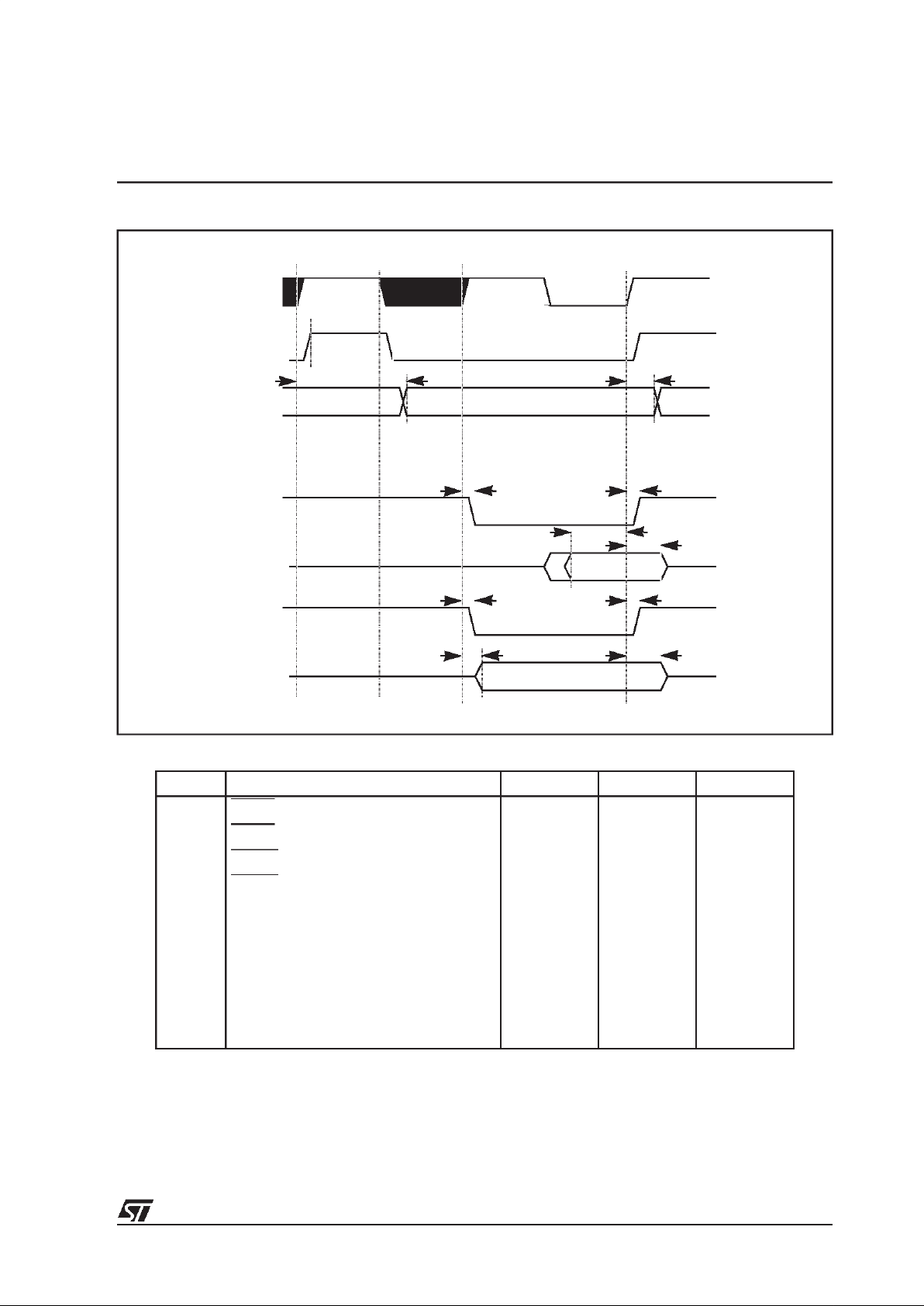
77/87
ST18-AU1
18.3.6 E-bus (Y BSU)
No PARAMETER Min (ns) Typ (ns) Max (ns)
t55 EYRD low delay 2.85
t56 EYRD high delay 1.4
t57 EYWR low delay 2.85
t58 EYWR high delay 1.4
t59 EA valid delay T0+4.1
t60 EA hold time T0+4.05
t61 ED (in) setup time 9.2
t62 ED (in) hold time -7.55
t63 ED (out) valid delay (Hi to Lo Z) 4.20
t64 ED (out) valid delay (Lo to Hi Z) 2.05
CLKOUT
INCYCLE
EYRD
EA
ED (in)
EYWR
ED (out)
t59 t60
t55
t56
t57
t58
t61
t62
t63
t64
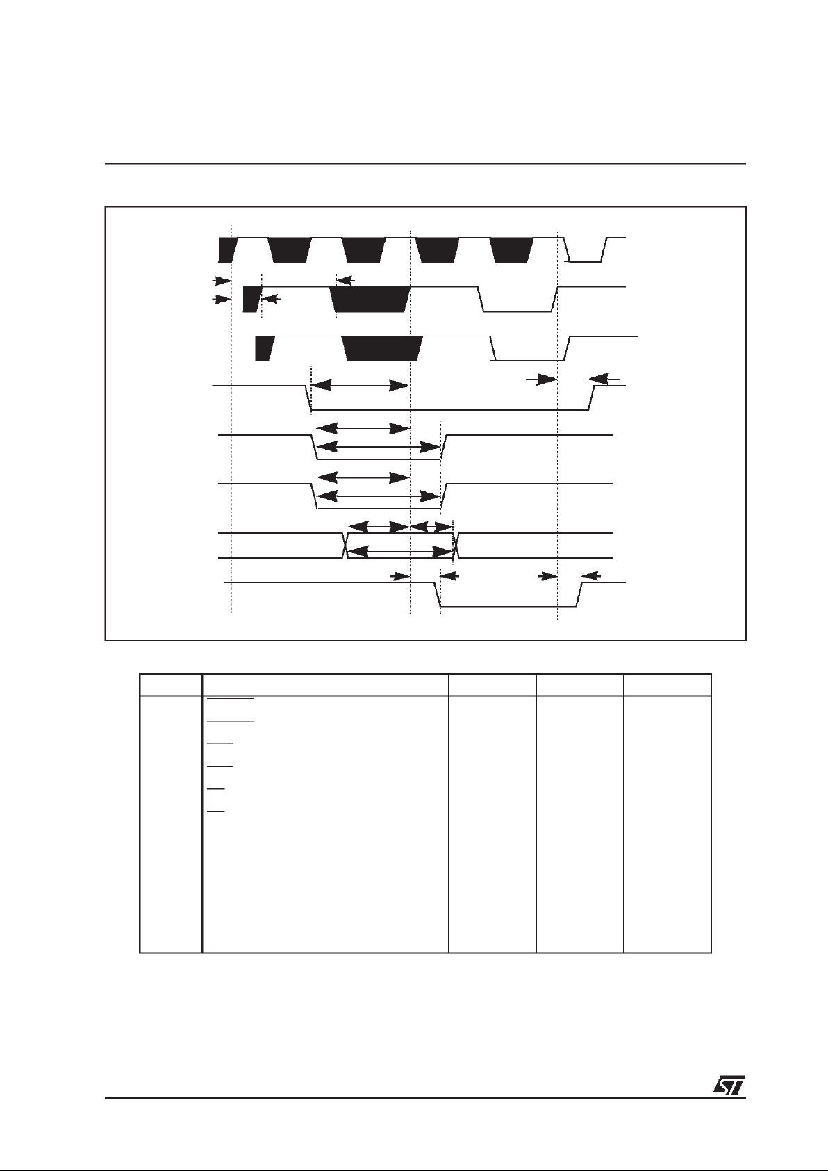
78/87
ST18-AU1
18.3.7 D950 control
No PARAMETER Min (ns) Typ (ns) Max (ns)
t65 RESET setup time 8.30
t66 RESET hold time
t67 IRQ setup time 6
t68 IRQ min. pulse duration,low
t69 LP setup time 6.2
t70 LP min. pulse duration,low
t71 P (in) setup time 6.05
t72 P (in) hold time -5.85
t73 P (in) min pulse duration,low (edge
t74 P (out ) low delay 2.6
t75 P (out ) high delay 3.0
CLK0
CLKOUT
IRQ
INCYCLE
P(in)
P(out)
t3
t4
t67
t71
t68
t74
RESET
LP
t65 t66
t69
t70
t72
t75
t73

79/87
ST18-AU1
18.3.8 I2C Host interface
* = External R load to Vdd =
** Rise time defined by External Rload
No PARAMETER Min (ns) Typ (ns) Max (ns)
t76 HDA(in) setup time vs SCLK 2xT0 + 1.1ns
t77 HDA(in) hold time vs SCLK 0
t78* HDA (out) low delay min 2xT0 + 6.45ns
HDA (out) low delay max 4xT0 + 6.45ns
t79** HDA (out) lo to Hi Z delay min TBD
HDA (out) lo to Hi Z delay max TBD
t80 START Condition setup TBD
t81 STOP Condition setup TBD
INCYCLE
SCL (in)
HDA (in)
t76
t77
t78
t79
HCL (in)
HDA (out)
HDA (out)
CLK0
2x T0
HCL (in)
t80
t81

80/87
ST18-AU1
18.3.9 PCM and SPDIF
* SCLKPCM generated from CLK1, Prescaler divide by 2
No PARAMETER Min (ns) Typ (ns) Max (ns)
t82* SCLKPCM high delay 10.3
t83* SCLKPCM low delay 10.4
t84 WSPCM high delay 11.4
t85 WSPCM low delay 11.30
t86 PCMOUT0/1/2 high delay 10.65
t87 PCMOUT0/1/2 low delay 10.60
t88 SPDIFOUT high delay 11.4
t89 SPDIFOUT low delay 11.3
CLK1
SCLK
SCLKPCM
t9
t10
t82 t83
t84 t85
WSPCM
t86 t87
t88
t89
PCMOUT0/1/2
SPDIFOUT
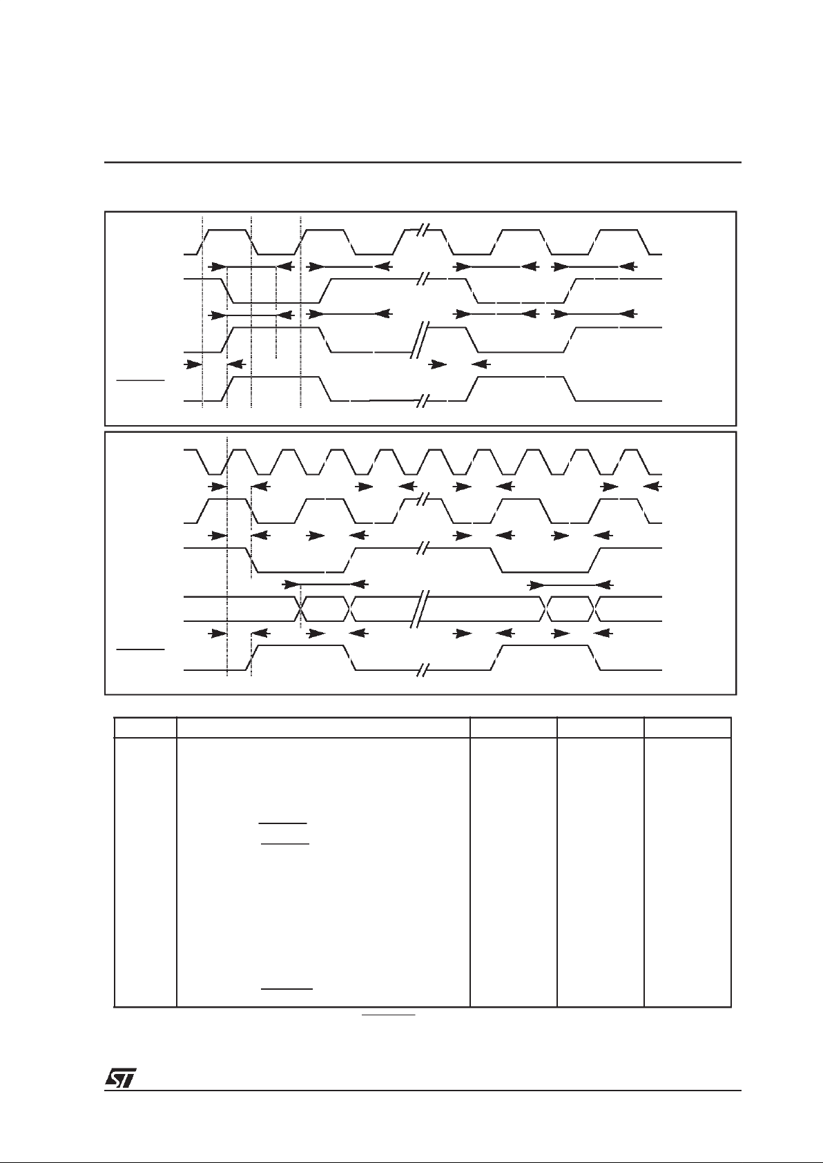
81/87
ST18-AU1
18.3.10 I2S Data Input 0
* For this time, CLKDIN0 ishalted by DREQ0.
No PARAMETER Min (ns) Typ (ns) Max (ns)
t90 WSDIN0 to CLKDIN0 setup time -1.45
t91 CLKDIN0 to WSDIN0 hold time 2.10
t92 DIN0 to CLKDIN0 setup time -2.95
t93 CLKDIN0 to DIN0 hold time 3.45
t94 CLKDIN0 to DREQ0 rise propagation time 7.05
t95* CLK0 rise to DREQ0 fall propagation time 12.90
t96 CLK1 rise to CLKDIN0 fall propagation time 9.70
t97 CLK1 rise to CLKDIN0 rise propagation time 9.90
t98 CLK1 rise to WSDIN0 fall propagation time 11
t99 CLK1 rise to WSDIN0 rise propagation time 10.95
t100 DIN0 to CLK1 rise setup time -4.80
t101 CLK1 rise to DIN0 hold time -5.40
t102 CLK1 rise to DREQ0 propagation time 10.90
CLKDIN0
WSDIN0
DIN0
t90
t92
DREQ0
t95t94 t94 t95
SLAVE MODE
CLKDIN0
WSDIN0
DIN0
DREQ0
MASTER MODE
CLK1
t96
t93
t92
t93
t97 t97 t96
t98 t99 t98 t99
t101t100
t101t100
t102 t102 t102 t102
t91 t90t91 t90t91t90t91
t92
t93
t92
t93

82/87
ST18-AU1
18.3.11 I2S Data Input 1
No PARAMETER Min (ns) Typ (ns) Max (ns)
t103 WSDIN1 to CLKDIN1 setup time -1.6
t104 CLKDIN1 to WSDIN1 hold time 1.4
t105 DIN1 to CLKDIN1 setup time -2.05
t106 CLKDIN1 to DIN1 hold time 2.35
t107 CLK1 rise to CLKDIN1 fall propagation time 9.50
t108 CLK1 rise to CLKDIN1 rise propagation time 9.50
t109 CLK1 rise to WSDIN1 fall propagation time 11.10
t110 CLK1 rise to WSDIN1 rise propagation time 11.15
t111 DIN1 to CLK1 rise setup time -4.25
t112 CLK1 rise to DIN1 hold time 4.56
CLKDIN1
WSDIN1
DIN1
t103
t105
SLAVE MODE
WSDIN1
CLKDIN1
DIN1
MASTER MODE
CLK1
t107
t106
t105
t106
t108 t108 t107
t109 t110 t109 t110
t112t111
t112t111
t104 t103t104 t103t104t103t104
t105
t106 t105t106

83/87
ST18-AU1
19 ST18-AU1 PACKAGE SPECIFICATIONS
19.1 ST18-AU1 package pinout
The ST18-AU1 is available in a 160 pin plasticquad flat pack (PQFP) package.
Table 19.1 ST18-AU1 package pinout
Pin name Pin no. Pin name Pin no. Pin name Pin no. Pin name Pin no.
GNDE
1
VDD
41
VDDE
81
GND
121
VDDE 2 GND 42 GNDE 82 VDD 122
IDE<15> 3 VDDE 43 EA<0> 83 P<7> 123
IDE<14>
4
GNDE
44
EA<1>
84
P<6>
124
IDE<13>
5
PCM_OUT0
45
EA_<2>
85
P<5>
125
IDE<12>
6
PCM_OUT1
46
EA<3>
86
P<4>
126
IDE<11>
7
PCM_OUT2
47
EA<4>
87
P<3>
127
IDE<10> 8 WSPCM 48 EA<5> 88 P<2> 128
IDE<9> 9 SCLKPCM 49 EA<6> 89 P<1> 129
IDE<8>
10
SPDIFOUT
50
EA<7>
90
P<0>
130
IDE<7>
11
IRDE
51
EA<8>
91
MODE_RESET
131
IDE<6>
12
IWRE
52
EA<9>
92
TDI
132
IDE<5>
13
GND
53
EA<10>
93
GND
133
IDE<4> 14 IBSE 54 VDDE 94 VDD 134
IDE<3> 15 INCYCLE 55 GNDE 95 IRQ 135
IDE<2>
16
CLKOUT
56
EA<11>
96
LP
136
IDE<1>
17
VDD
57
EA<12>
97
SCLK
137
GNDE
18
GND
58
EA<13>
98
HSAS
138
VDDE
19
VDD
59
EA<14>
99
HDA
139
VDD 20 GND 60 EA<15> 100 HCL 140
IDE<0> 21 MCLK_MODE 61 ED<0> 101 DREQ0 141
IAE<15>
22
CLK0
62
ED<1>
102
CLKDIN1
142
GND
23
CLK1
63
ED<2>
103
CLKDIN0
143
IAE<14>
24
CLK0_MODE
64
ED<3>
104
WSDIN1
144
IAE<13>
25
CLK1_MODE
65
ED<4>
105
WSDIN0
145
IAE<12> 26 PLL_MODE 66 VDDE 106 DIN1 146
IAE<11> 27 EXTAL0 67 GNDE 107 VDD 147
IAE<10>
28
VDD
68
ED<5>
108
GND
148
IAE<9>
29
EXTAL1
69
ED<6>
109
DIN0
149
IAE<8>
30
XTAL0
70
ED<7>
110
SNAP
150
IAE<7>
31
XTAL1
71
ED<8>
111
HALTACK
151
IAE<6> 32 XBSE 72 ED<9> 112 IDLE 152

84/87
ST18-AU1
19.2 160 pin PQFP package dimensions
Table 19.2 160 pin PQFP package dimensions
IAE<5> 33 XRDE_EXRD 73 ED<10> 113 ERQ 153
IAE<4>
34
XWRE_EXWR
74
ED<11>
114
RESET
154
IAE<3>
35
EYWR
75
ED<12>
115
TMS
155
IAE<2>
36
EIWR
76
ED<13>
115
TDO
156
IAE<1>
37
EIRD
77
ED<14>
117
TCK
157
IAE<0> 38 EYRD 78 ED<15> 118 TRST 158
GNDE 39 VDD 79 VDDE 119 GND 159
VDDE
40
GND
80
GNDE
120
VDD
160
REF. TYP MIN MAX
A 4,07
A1 0,25
A2 3,42 3,17 3,67
B 0,22 0,38
c 0,13 0,23
D 31,20 30,95 31,45
D1 28,00 27,90 28,10
D3 25,35
e 0,65
E 31,20 30,95 31,45
E1 28,00 27,90 28,10
E3 25,35
L 0,80 0,65 0,95
L1 1,60
k0°7°
Pin name Pin no. Pin name Pin no. Pin name Pin no. Pin name Pin no.

85/87
ST18-AU1
Figure 19.1 Package diagram

86/87
ST18-AU1
20 DEVICE ID
The identification code for the ST18-AU1 is#m52BD041, wheremis a manufacturing revision
number reserved by SGS-THOMSON.
21 ORDERING INFORMATION
For further information contact your local SGS-THOMSON sales office.
bit 31 bit 0
Mask rev ST18 family Variant SGS-THOMSON manufacturers
id
1)
1) Defined as 1 in IEEE 1149.1 standard.
reserved 0 1 0 1 0 0 1 0 1 0 1 1 1 1 0 1 0 0 0 0 0 1 0 0 0 0 0 1
52BD041
Device Package
ST18AU1X??S 160 pin plastic quad flat pack (PQFP)

87/87
Notes
Information furnished is believed to be accurate and reliable. However, SGS-THOMSON Microelectronics assumes no responsibility for the
consequences of use of such information nor for any infringement of patents or other rights of third parties whichmay result from its use. No
license is granted by implication or otherwise under any patent or patent rights of SGS-THOMSON Microelectronics. Specifications
mentioned in this publication are subject to change without notice. This publication supersedes and replaces all information previously
supplied. SGS-THOMSON Microelectronics products are not authorized for use as critical components in life support devices or systems
without the express written approval of SGS-THOMSONMicroelectronics.
1997 SGS-THOMSON Microelectronics - All rights reserved.
SGS-THOMSON Microelectronics Group of Companies
Australia - Brazil - Canada - China - France - Germany - Italy - Japan - Korea - Malaysia - Malta - Morocco - The Netherlands - Singapore -
Spain -Sweden - Switzerland - Taiwan - Thailand -United Kingdom - U.S.A.
4
 Loading...