

■ GLITCH FREE TRANSITION BETWEEN
INPUT SOURCES
■ INTERNAL LOGIC SELECTS INPUT
SOURCE
■ GATE DRIVE FOR EXTERNAL PMOS
BYPASS SWITCH
■ 5V DETECTOR WITH HYSTERESIS
■ 1% 3.3V REGULATED OUTPUT VOLTAGE
■ 500mA GUARANTEED OUTPUT CURRENT
■ OPERATING TEMPERATURE RANGE
FROM 0°C TO 85°C
■ AVAILABLE IN P
■ PPAK AND SO-8 PACKAGES CAN BE
2
PAK PACKAGE
AVAILABLE ON REQUEST
APPLICATIONS
■ NETWORK INTERFACE CARDS
■ PCMCIA/PCI INTERFACE CARDS
■ DESKTOP COMPUTERS
■ POWER SUPPLY WITH MULTIPLE INPUT
SOURCES
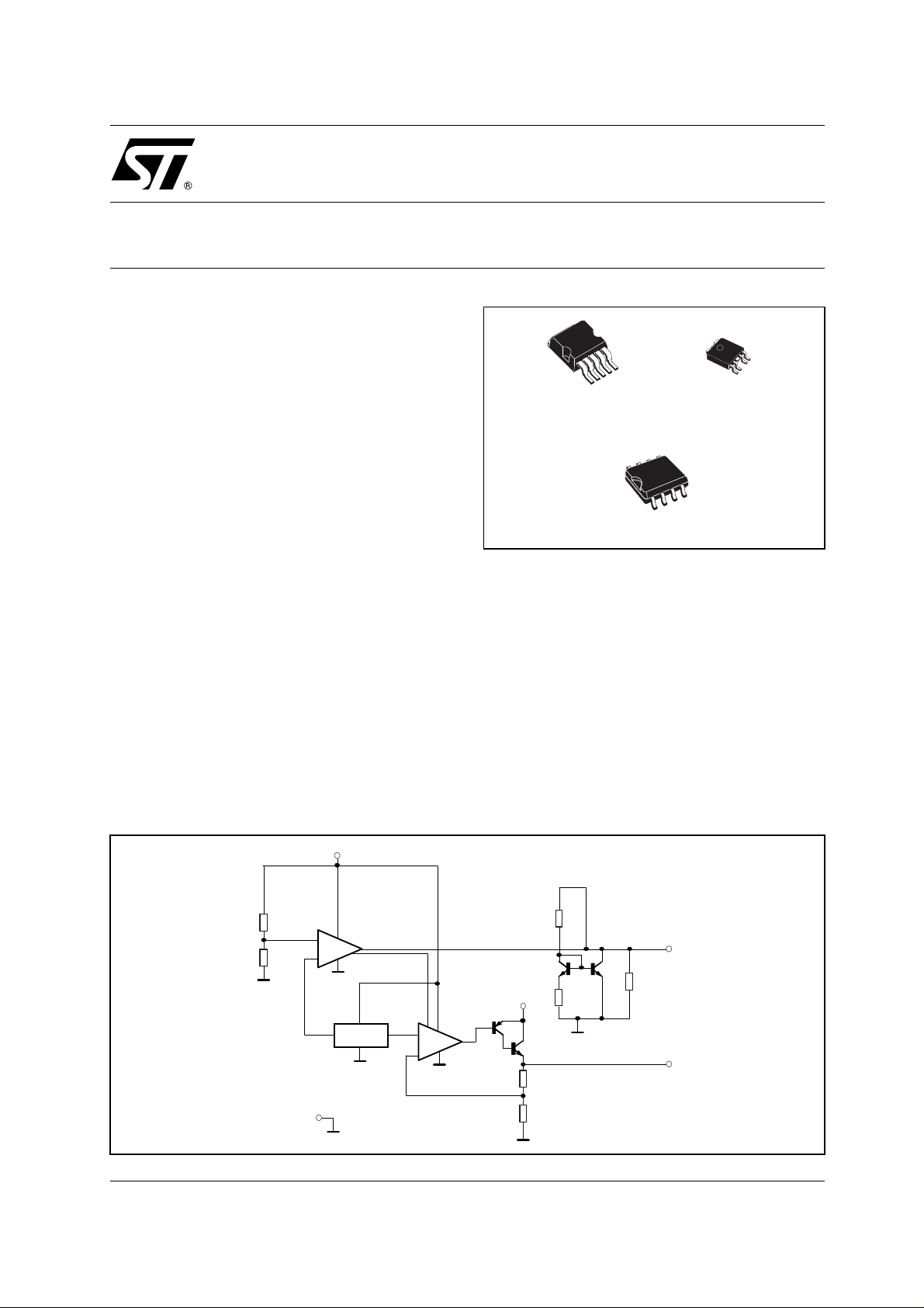
DESCRIPTION
The ST1534A is intended for app lication such as
power managed PCI and network interface cards
(NICs), where operations from 3.3V V AUX supply
SCHEMATIC DIAGRAM
ST1534A
500mA SMART LDO
PPAKP2PAK
SO-8
may be required when the 5V supply has been
shut down.
During regular operation, 3.3V power f or the PCI
card is provided by the internal LDO regulator,
generated from 5V supply. When the 5V V
available, the IC connects thissupply directlyto its
output using an external P-Channel FET. This
ensures an uninterrupted 3. 3V out even if VIN falls
out of specificat ion.
When both supplies are available simultaneously,
the drive p in DR will be pulled high, turning off the
PMOS switch.
The device is available in the popular 5 leads
2
P
PAK and PPA K
AUX
is
+
5V Detect
-
GND
VIN
Reference
+
Error
Amp
-
VIN
Rpull_down
V
OUT
DR
1/15April 2003
ST1534A
ABSOLUTE MAXIMUM RATINGS
Symbol Parameter² Value Unit
V
V
SHDN
I
T
T
Absolute Maximum Ratings are those values beyond which damage to the device may occur. Functional operation under these condition is
not implied.
THERMAL DATA
DC Input Voltage
I
Shutdown Input Voltage
Output Current
O
Storage Temperature Range
stg
Operating Junction Temperature Range
op
-0.3 to 7 V
-0.3 to 7 V
Internally limited mA
-40 to +125 °C
0to+85 °C
Symbol Parameter PPAK
R
thj-case
R
thj-amb
Thermal Resistance Junction-case
Thermal Resistance Junction-ambient
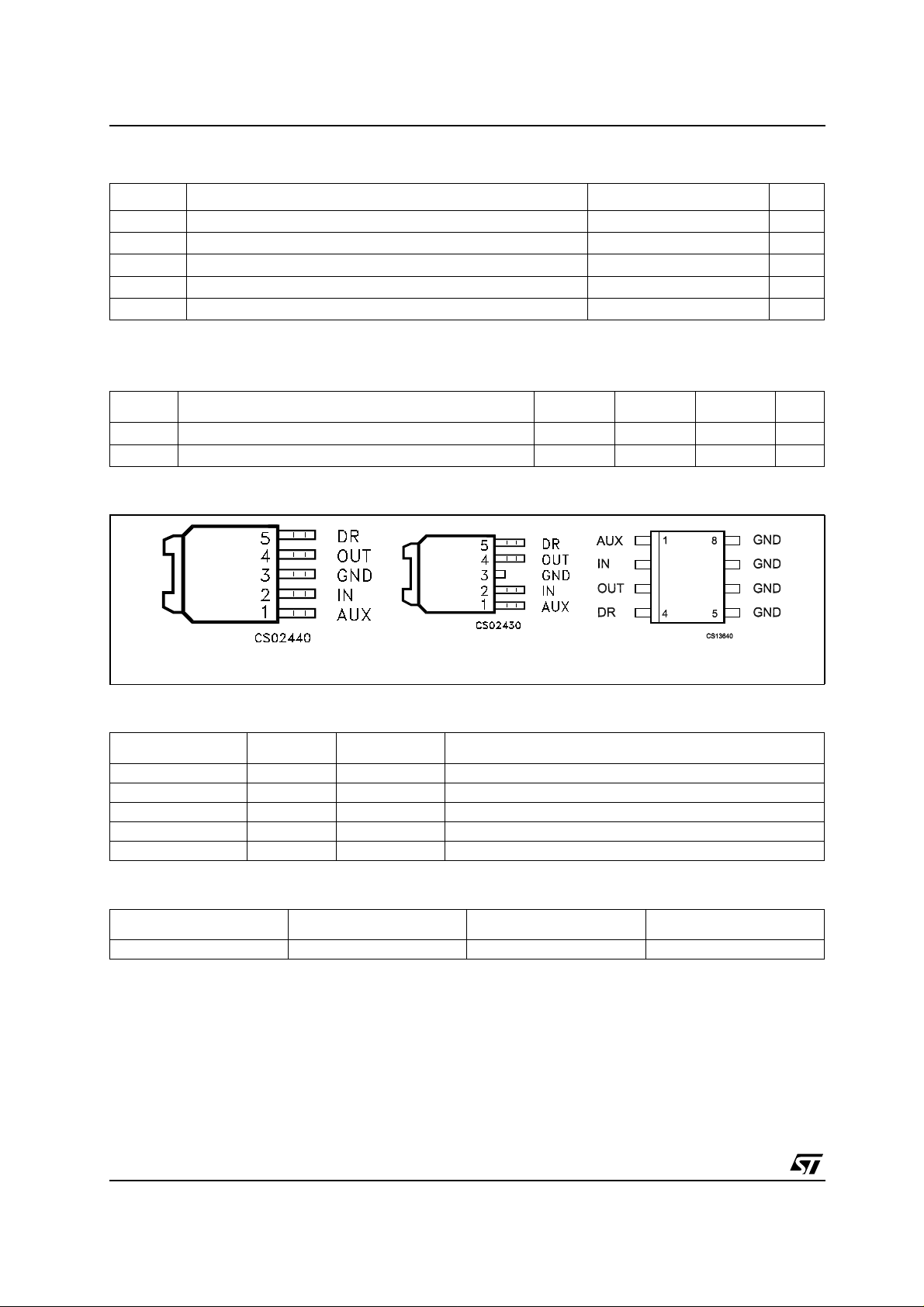
CONNECTION DIAGRAM (top view)
2
PAK
P
PPAK
PIN DESCRIPTION
Pin PPAK/P
1 1 AUX Auxiliary Input port typically 3.3V
2 2 IN Input port typically 5V
3 5, 6, 7, 8 GND Ground
4 3 OUT LDO 3.3V Output Port
5 4 DR Drive Output for external P-Channel MOSFET pass element
2
PAK
Pin SO/8 Symbol Name and Function
2
PAK
P
SO-8 Unit
8320°C/W
100 50 55 °C/W
SO-8
ORDERING INFORMATION
TYPE PPAK (*)
ST1534A ST1534APT ST1534AP2T ST1534AD
(*) PPAK and SO-8 a re availablein Tape & Reel with the suffix"-TR".
2
(#) P
PAKisavailableinTape&Reelwiththesuffix"-R".
2/15
2
PAK (#)
P
SO-8 (*)
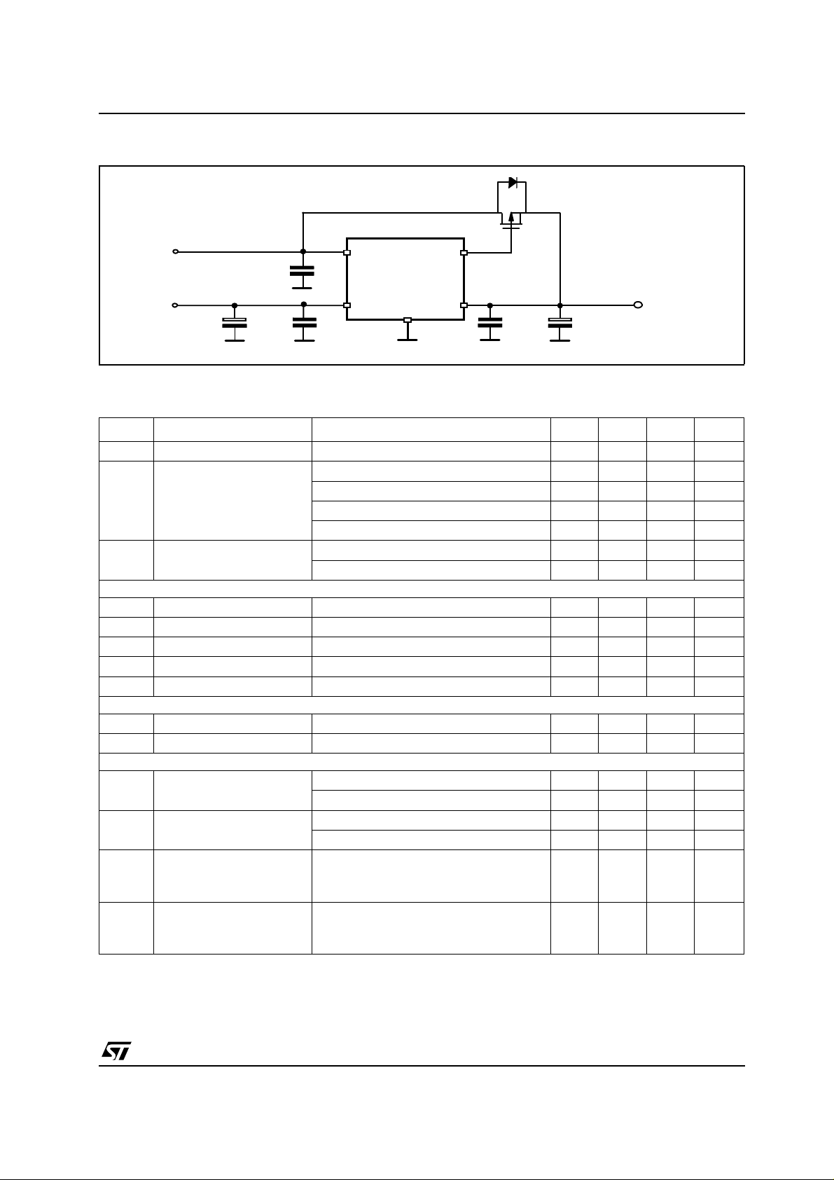
TYPICAL APPLICATION CIRCUIT
ST1534A
3.3V
0.1 µF
5V
4.7 µF 0.1 µF
ELECTRICAL CHARACTERISTICS (T
AUX
IN
GND
=25°C,VI=5V, V
j
DR
OUT
10 µF0.1 µF
=3.3V, IO=10mA, CO=2.2µF,
AUX
Vout=3.3V
unless otherwise spec ified)
Symbol Parameter Test Conditions Min. Typ. Max. Unit
Input Voltage Range 4.5 5 5.5 V
V
I
Input Supply Current VI≥ 4.5V IO= 0mA V
I
IN
I
Auxliary Supply Current VI= 0 V 2.2 mA
AUX
3.3V VOLTAGE REGULATOR BLOCK
V
Output Voltage Tj= 0 to 85 °C 3.18 3.3 3.42 V
O
∆V
∆V
Line Regulation VI= 4.5 to 5.5V 0.04 0.5 %
O
Load Regulation IO= 0 to 500mA 0.1 1 %
O
Dropout Voltage IO= 500 mA Tj= 0 to 85 °C 1.15 V
V
d
Output Current Limit Tj=0to85°C 550 mA
I
O
5V DETECT BLOCK
V
V
Low Threshold Voltage VIfalling, IO= 500 mA Tj= 0 to 85 °C 4.15 4.3 V
THL
Hysteresis 70 200 mV
HYST
DRIVE OUTPUT BLOCK
V
Note 1: Guaranteed by design
Note 2: See timing diagram
Drive Output Voltage VI= 4.5 to 5.5V IDR=200µA 3.6 VIN-0.8 V
DR
Drive Current Sinking: VI= 4.15V VDR= 1V 7 20 mA
I
DR
Drive High Delay (Note 1
t
DH
and 2)
Drive Low Delay (Note 1
t
DL
and 2)
≥4.5V IO= 0mA V
V
I
< 4.1V IO= 0mA V
V
I
< 4.1V IO= 0mA V
V
I
V
= 5V 200 µA
I
< 4.15V IDR=200µA 100 200 mV
V
I
Sourcing: V
= 4.5V VI-VDR= 2V 7 25 mA
I
CDR= 1.2nF,VINramping up, measured
from V
I=VTH(H)
=0to85°C
T
j
to VDR= 3.3V
CDR= 1.2nF,VINramping down, measured
from V
I=VTH(L)
T
=0to85°C
j
to VDR= 200mV
=0V 11 mA
AUX
= 3.3V 11 mA
AUX
=0V 2 mA
AUX
= 3.3V 2 mA
AUX
25µs
36µs
3/15
ST1534A
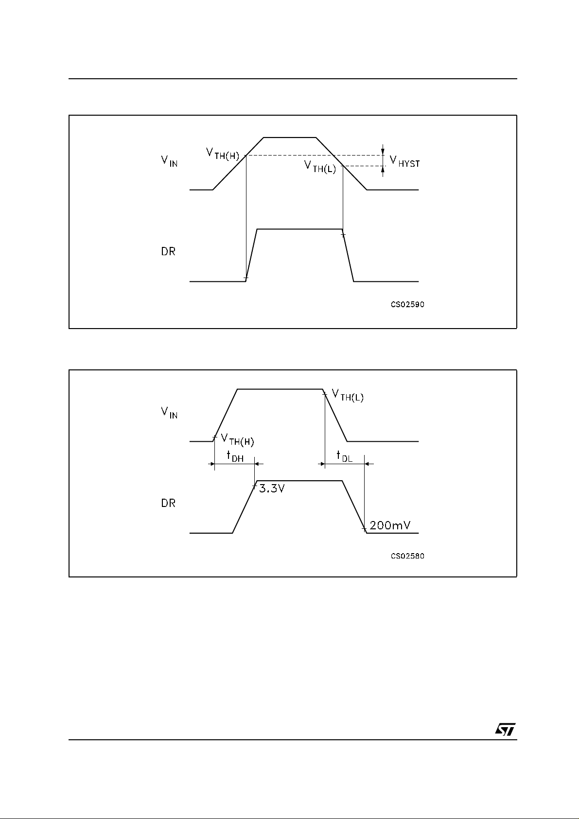
5V DETECT THRESHOLDS
VINrise and fall times (10% to 90%) to be > 100µs
TIMING DIAGRAM
VINrise and fall times (10% to 90%) to be > 100µs
4/15
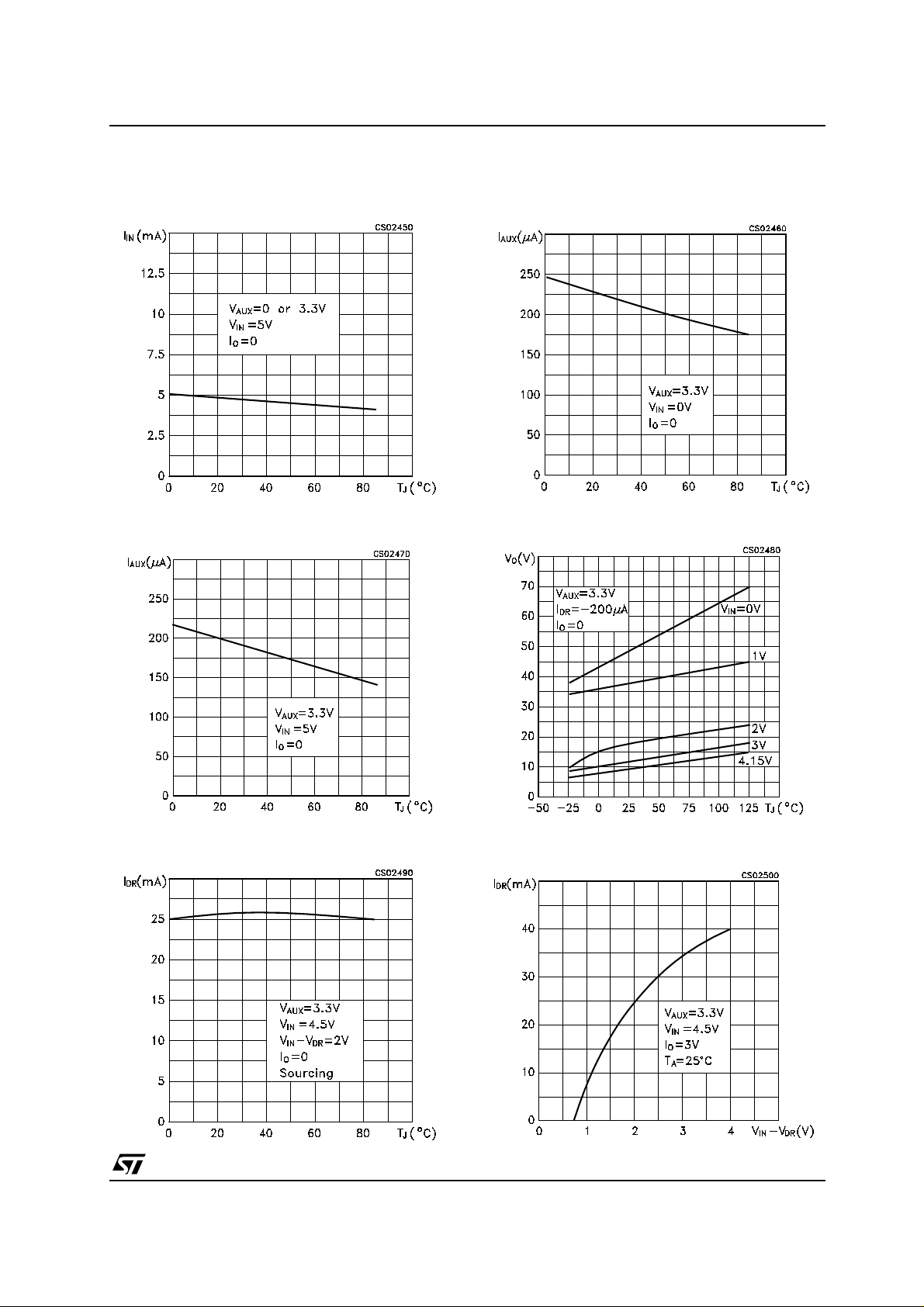
TYPICAL CHARACTERISTICS (unless otherwise specified Tj=25°C)
ST1534A
Figure1 : Supply Currentvs Temperature
Figure2 : Aux Current vs Temperature
Figure4 : Aux Current vs Temperature
Figure5 : Drive Output Voltage vs Tem perature
Figure3 : Drive Current vs Temperature
Figure6 : Drive Current vs V
IN-VDR
5/15

ST1534A
Figure7 : Drive Current vs Temperature
Figure8 : Line Regulation vs Temperature
Figure10 : Output Voltage vs Temperature
Figure11 : Load Regulation vs Tem perat ure
Figure9 : Output Voltage vs Input Voltage
6/15
Figure12 : Threshold Voltage vs Temperature

ST1534A
V
100
I
C
V
I
C
l
V
100
dC
V
I
C
l
V
I
C
C
Figure13 : Hysteresis vs Temperature
Figure14 : Threshold
Figure16 : Threshold
=3.5 to4.5V,ts=tf>
I
=33+0.1µF
C
O
µs,NoLoa
Figure17 : Glitch
=0.1+4.7µF,
I
=3.5 to4.5V,ts=tf>
I
=33+0.1µF
C
O
Figure15 : Glitch
=3.5 to 5V,
I
=500mA,
O
µs,
=500mA,
O
=33+0.1µF,withP-Channe
O
=0.1+4.7µF,
I
=3.5 to 5V,
I
=500mA,
O
=33+0.1µF,withP-Channe
O
Figure18 : Line Transient
=4.5 to 5.5V,
I
=0.1µF,
C
AUX
=10mA,
O
=0.1+4.7µF,
I
=33+0.1µF,
O
7/15

ST1534A
V
I
C
C
C
F
Figure19 : Load Transient
=5V,
I
=0to 500mA,
O
=4.7+0.1µF,
I
=0.1+33µF,
O
AUX
=0.1µ
8/15

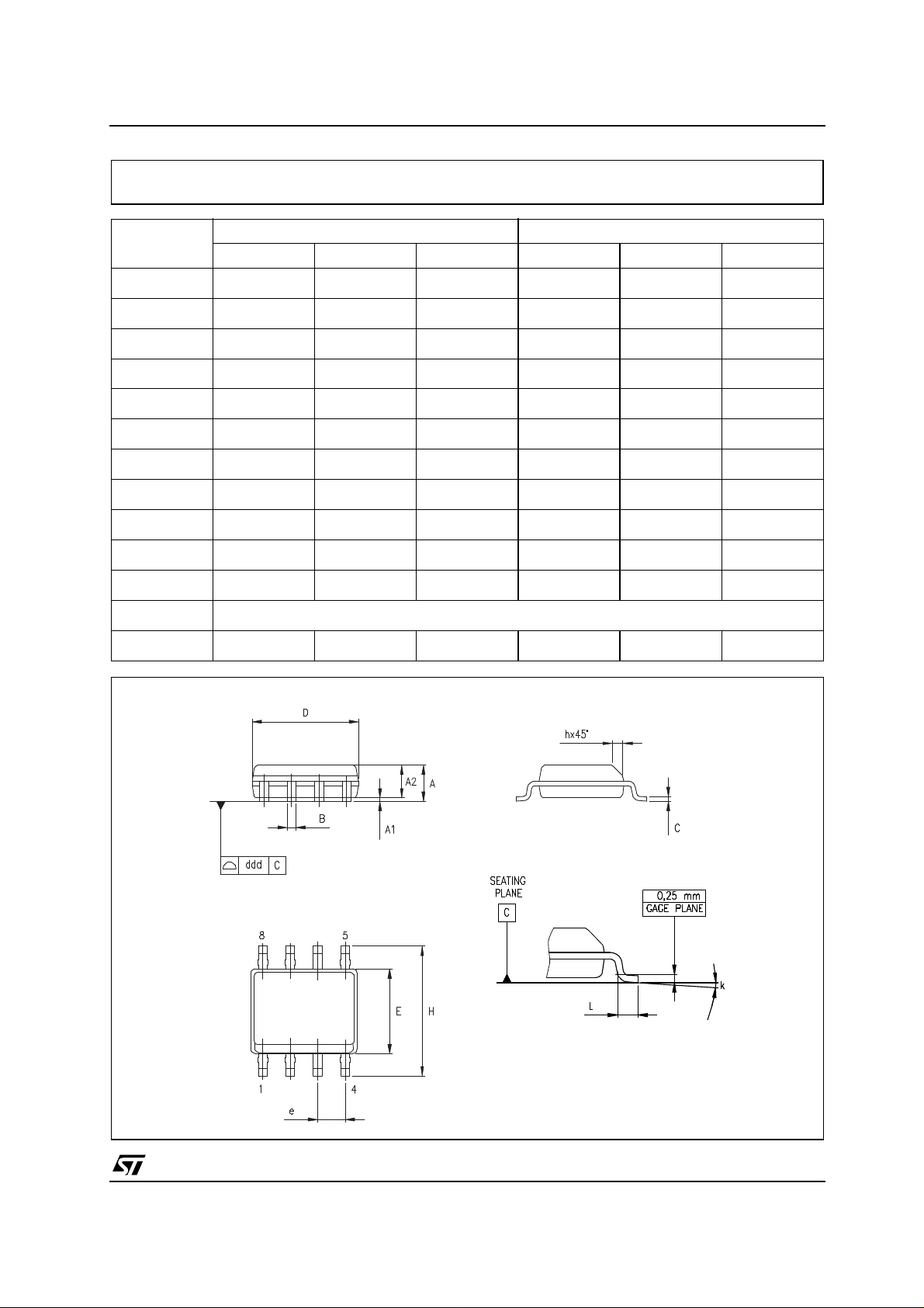
PPAK MECHANICAL DATA
ST1534A
DIM.
MIN. TYP MAX. MIN. TYP. MAX.
A 2.2 2.4 0.086 0.094
A1 0.9 1.1 0.035 0.043
A2 0.03 0.23 0.001 0.009
B 0.4 0.6 0.015 0.023
B2 5.2 5.4 0.204 0.212
C 0.45 0.6 0.017 0.023
C2 0.48 0.6 0.019 0.023
D 6 6.2 0.236 0.244
E 6.4 6.6 0.252 0.260
G 4.9 5.25 0.193 0.206
G1 2.38 2.7 0.093 0.106
H 9.35 10.1 0.368 0.397
L2 0.8 0.031
L4 0.6 1 0.023 0.039
mm. inch
0078180-B
9/15

ST1534A
P2PAK/A MECHANICAL DATA
DIM.
MIN. TYP MAX. MIN. TYP. MAX.
A 4.30 4.80 0.169 0.188
A2 0.03 0.23 0.001 0.009
C 1.17 1.37 0.046 0.053
D 2.40 2.80 0.094 0.110
D1 8.95 9.35 0.352 0.368
E 0.45 0.60 0.017 0.023
F 0.80 1.05 0.031 0.041
G 3.20 3.60 0.126 0.142
G1 6.60 7.00 0.260 0.275
H1 8.5 0.334 0.409
H2 10.00 10.40 0.393 0.409
L 15 15.85 0.590 0.624
L1 8 0.315
L2 1.27 1.40 0.050 0.055
M 2.4 3.2 0.094 0.126
R 0.40 0.016
V2 0˚ 8˚ 0˚ 8˚
mm. inch
10/15
7157127/A
SO-8 MECHANICAL DATA
ST1534A
DIM.
A 1.35 1.75 0.053 0.069
A1 0.10 0.25 0.04 0.010
A2 1.10 1.65 0.043 0.065
B 0.33 0.51 0.013 0.020
C 0.19 0.25 0.007 0.010
D 4.80 5.00 0.189 0.197
E 3.80 4.00 0.150 0.157
e 1.27 0.050
H 5.80 6.20 0.228 0.244
h 0.25 0.50 0.010 0.020
L 0.40 1.27 0.016 0.050
k ˚ (max.)
ddd 0.1 0.04
MIN. TYP MAX. MIN. TYP. MAX.
mm. inch
8
0016023/C
11/15
ST1534A
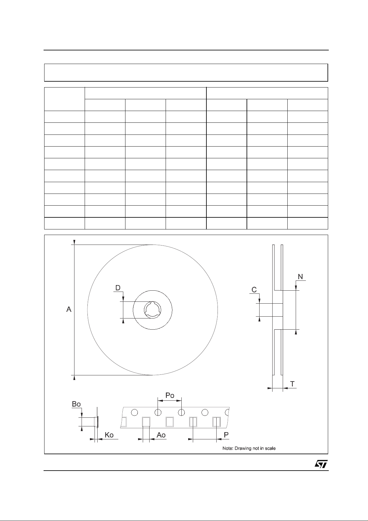
Tape & Reel DPAK-PPAK MECHANICAL DATA
DIM.
MIN. TYP MAX. MIN. TYP. MAX.
A 180 7.086
C 12.8 13.0 13.2 0.504 0.512 0.519
D 20.2 0.795
N 60 2.362
T 14.4 0.567
Ao 6.80 6.90 7.00 0.268 0.272 0.2.76
Bo 10.40 10.50 10.60 0.409 0.413 0.417
Ko 2.55 2.65 2.75 0.100 0.104 0.105
Po 3.9 4.0 4.1 0.153 0.157 0.161
P 7.9 8.0 8.1 0.311 0.315 0.319
mm. inch
12/15
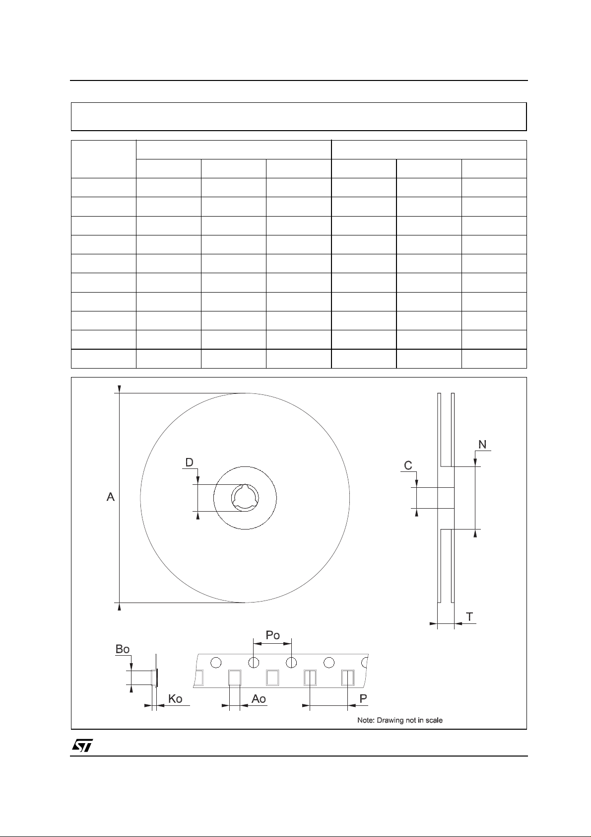
ST1534A
Tape & Reel D
DIM.
A 180 7.086
C 12.8 13.0 13.2 0.504 0.512 0.519
D 20.2 0.795
N 60 2.362
T 14.4 0.567
Ao 10.50 10.6 10.70 0.413 0.417 0.421
Bo 15.70 15.80 15.90 0.618 0.622 0.626
Ko 4.80 4.90 5.00 0.189 0.193 0.197
Po 3.9 4.0 4.1 0.153 0.157 0.161
P 11.9 12.0 12.1 0.468 0.472 0.476
2
PAK-P2PAK-D2PAK/A-P2PAK/A MECHANICAL DATA
mm. inch
MIN. TYP MAX. MIN. TYP. MAX.
13/15

ST1534A
Tape & Reel SO-8 MECHANICAL DATA
mm. inch
DIM.
MIN. TYP MAX. MIN. TYP. MAX.
A 330 12.992
C 12.8 13.2 0.504 0.519
D 20.2 0.795
N 60 2.362
T 22.4 0.882
Ao 8.1 8.5 0.319 0.335
Bo 5.5 5.9 0.216 0.232
Ko 2.1 2.3 0.082 0.090
Po 3.9 4.1 0.153 0.161
P 7.9 8.1 0.311 0.319
14/15

ST1534A
Information furnished is believed to be accurate and reliable. However, STMicroelectronics assumes no responsibility for the
consequences of use o f suc h inf ormat ion n or f or an y infr ingeme nt of paten ts or oth er ri gh ts of third part ies whic h may resul t f rom
its use. No license is granted by implication or otherwise under any patent or patent rights of STMicroelectronics. Specifications
mentioned in this publication are subject to change without notice. This publication supersedes and replaces all information
previously supplied. STMicroelectronics products are not authorized for use as critical components in life support devices or
systems without express written approval of STMicroelectronics.
Australia - Brazil - Canada - China - Finland - France - Germany - Hong Kong - India - Israel - Italy - Japan - Malaysia - Malta - Morocco
© The ST logo is a registered trademark of STMicroelectronics
© 2003 STMicroelectronics - Printed in Italy - All Rights Reserved
STMicroelectronics GROUP OF COMPANIES
Singapore - Spain - Sweden - Switzerland - United Kingdom - United States.
© http://www.st.com
15/15
 Loading...