

Datasheet ST10F269Z2QX, ST10F269Z2Q6, ST10F269Z2Q3 Datasheet (SGS Thomson Microelectronics)
ST10F269Z2Qx
16-BIT MCU WITH MAC UNIT, 256K BYTE FLASH MEMORY AND 12K BYTE RAM
PRELIMINARY DATA
■ HIGH PERFORMANCE 40MHz CPU WITH DSP
FUNCTION
– 16-BIT CPU WITH 4-STAGE PIPELINE
– 50ns INSTRUCTION CYCLE TIME AT 40MHz MAX
CPU CLO CK
– MULTIPLY/ACCUMULATE UNIT (MAC) 1 6 x 16-B IT
MULTIPLICATION, 40-BIT ACCUMULATOR
– REPEAT UNIT
– ENHANCED BO OLEAN BIT MANIPULATION FA-
CILITIE S
– ADDITIONAL INST RUC TIONS TO SUPP ORT HL L
AND OPERATING SYSTEMS
– SINGLE-CYCLE CONTEXT SWITCHING SUP-
PORT
■ MEMORY ORGANIZATION
– 256K BYTE ON-CHIP FLASH MEMORY SINGLE
VOLTAGE WITH ERASE/PROGRAM CONTROLLER
– UP TO 1K ERASING/PROGRAMMI NG CYCLES
– UP TO 16M BYTE LIN EAR AD DRE SS SPAC E FOR
CODE AN D DATA (5 M BYTES WITH CAN)
– 2K BYT E ON-CHIP INTE RNAL RAM (IRAM)
– 10K BYTE ON-CHIP EXTENSION RAM (XRAM)
■ FAST AND FLEXIBLE BUS
– PROGRAMMABLE EXTERNAL BUS CHARACTE-
RISTICS FOR DIFFERENT ADDRESS RANGES
– 8-BIT O R 16-BIT EXTERNAL DATA BUS
– MULTIPLE XE D O R DE MU LT IP LE XED E XT ER N AL
ADDRESS/DA TA BUSES
– FIVE PROGRAMMABLE CHIP-SELECT SIGNALS
– HOLD-A CK NOW L E DG E BU S ARBITRATION SUP-
PORT
■ INTERRUPT
■ TWO CAN 2.0B INTERFACES OPERATING ON
ONE OR TWO CAN BUSSES (30 OR 2x15
MESSAGE OBJECTS)
■ FAIL-SAFE PROTECTION
– PROGRA MMABLE WATCHDOG TIMER
– OSCILLATOR WATCHDOG
■ ON-CH IP BOOTSTRAP LOADER
■ CLOCK GENERATION
– ON-CHIP PLL
– DIRECT OR PRESCALED CLOCK INPUT
■ REAL TIM E CLO CK
■ UP TO 111 GENERAL PURPOSE I/O LINES
– INDIVIDUALLY PROGRAMMABLE AS INPUT,
OUTPUT OR SPECIAL FUNCTION
– PROGRAMMABLE THRESHOLD (HYSTERESIS)
■ IDLE AN D POWER DOWN M ODES
■ SINGLE VOLTAGE SUPPLY: 5V ±10% (EMBEDDED
REGULATOR FOR 3.3 V CO RE SUPPLY).
■ TEMPERATURE RANGES: -40 +125
■ 144-PIN PQFP PACKAGE
– 8-CHANNEL PERIPHERAL E VENT CONTROLLER
FOR SING LE CYCLE INTERRUPT DRIVEN DATA
TRANSFER
– 16-PRIOR ITY - LE VEL I NT ERR UP T SY ST EM W ITH
Flash Memory
56 SOURCES, SAMPLING RATE DOWN TO 25ns
■ TIMERS
– TWO MULTI-FUNCTIONAL GENERAL PURPOSE
TIMER UNITS WITH 5 TI M ERS
■ TWO 16-CHANNEL CAPTURE / COMPARE UNITS
■ A/D CONVERTER
CAN1_RX D
CAN1_TX D
CAN2_RX D
CAN2_TX D
10K Byte
XRAM
– 16-CHANNEL 10-BIT
– 4.85µs CONVERSION TIME AT 40MHz CPU CLOCK
■ 4-CHAN NEL PWM UNIT
■ SERIAL CHANNELS
– SYNCHRONOUS / ASYNCHRONOUS SERIAL
CHANNEL
– HIGH-SPEED SYNCHRONOUS CHANNEL
August 2002
This is prelim i nary inform ation on a new produc t now in dev el opment or und ergoing evaluation. Det ai l s are subject to change without notice.
PQFP144 (28 x 28 mm)
(Plastic Quad Flat Pack)
256K Byte
CAN1
CAN2
16
16
8
32
16
Port 0Port 1Port 4
Controller
10-Bit ADC
External Bus
Port 6 Port 5 Port 3
8
16 15
CPU-Core and MAC Unit
Interrupt Controller
GPT1
ASC usart
BRG
GPT2
PEC
SSC
BRG
°
C, -40 to 85°C
16
16
XTAL1 XTAL2
16
3.3V
PWM
CAPCOM2
CAPCOM1
Port 7 Port 8
8
2K Byte
Internal
RAM
Watchdog
Oscillator
and PLL
Voltage
Regulator
8
Port 2
16
1/161

ST10F269Z2Qx
TABLE OF CONTENTS PAGE
1 - INTRODUCTION ........... ............................................................................................. 6
2 - PIN DATA ................................................................................................................... 7
3 - FUNCTIONAL DESCRIPTION .............................. ........................ ............................. 13
4 - MEMORY ORGANIZATION ....................................................................................... 14
5 - INTERNAL FLASH MEMORY ........................................ ...................................... ..... 17
5.1 - OVERVIEW ................................................................................................................ 17
5.2 - OPERATIONAL OVERVIEW ...................................................................................... 17
5.3 - ARCHITECTURAL DESCRIPTION ............................................................................ 19
5.3.1 - Read Mode ................................................................................................................. 19
5.3.2 - Command Mode ......................................................................................................... 19
5.3.3 - Ready/Busy Signal ..................................................................................................... 19
5.3.4 - Flash Status Register ................................................................................................. 19
5.3.5 - Flash Protection Register ........................................................................................... 21
5.3.6 - In structions Description .............................................................................................. 21
5.3.7 - Reset Processing and Initial State .............................................................................. 25
5.4 - FLASH MEMORY CONFIGURATION ........................................................................ 25
5.5 - APPLICATION EXAMPLES ....................................................................................... 25
5.5.1 - Handling of Flash Addresses .. .................................................................................... 25
5.5.2 - Basic Flash Access Control ........................................................................................ 26
5.5.3 - Programming Examples ............................................................................................. 27
5.6 - BOOTSTRAP LOADER ............................................................................................ 30
5.6.1 - Entering the Bootstrap Loader .................................................................................... 30
5.6.2 - Memo ry Configuration After Reset ............................................................................. 31
5.6.3 - Loading the Startup Code ........................................................................................... 32
5.6.4 - Exiting Bootstrap Loader Mode .................................................................................. 32
5.6.5 - Choosing the Baud Rate for the BSL ......................................................................... 33
6 - CENTRAL PROCESSING UNIT (CPU) ..................................................................... 34
6.1 - MULTIPLIER-ACCUMULATOR UNIT (MAC) ............................................................. 35
6.1.1 - Features ..................................................................................................................... 36
6.1.1.1 - Enhanced Addressing Capab ilit ies.............................................................................. 36
6.1.1.2 - Multiply-Accumulate Unit............................................................................................. 36
6.1.1.3 - Program Control...... .................................................................................................... 36
6.2 - INSTRUCTION SET SUMMARY ................................................................................ 37
6.3 - MAC COPROCESSOR SPECIFIC INSTRUCTIONS ................................................. 38
7 - EXTERNAL BUS CONTROLLER ................................... ...................................... ..... 42
7.1 - PROGRAMMABLE CHIP SELECT TIMING CONTROL ............................................ 42
7.2 - READY PROGRAMMABLE POLARITY ..................................................................... 42
2/161

ST10F269Z2Qx
TABLE OF CONTENTS PAGE
8 - INTERRUPT SYSTEM ......... ...................................................................................... 44
8.1 - EXTERNAL INTERRUPTS ......................................................................................... 44
8.2 - INTERRUPT REGISTERS AND VECTORS L OCATION LIST .................................. 45
8.3 - INTERRUPT CONTROL REGISTERS ....................................................................... 46
8.4 - EXCEPTION AND ERR OR TRAPS LIST ................................................................... 47
9 - CAPTURE/COMPARE (CAPCOM) UNITS ................................................................ 48
10 - GENERAL PURPOSE TIM ER UNIT .......................................................................... 51
10.1 - GPT1 .......................................................................................................................... 51
10.2 - GPT2 .......................................................................................................................... 52
11 - PWM MODULE .......................................................................................................... 54
12 - PARALLEL PORTS ......... .......................................... ................................................ 55
12.1 - INTRODUCTION ........................................................................................................ 55
12.2 - I/O’S SPECIAL FEATURES ....................................................................................... 57
12.2.1 - Open Drain Mode ....................................................................................................... 57
12.2.2 - Input Threshold Control ............................................................................................ 57
12.2.3 - Output Driver Control ................................................................................................58
12.2.4 - Alternate Port Functions ............................................................................................. 60
12.3 - PORT0 ........................................................................................................................ 61
12.3.1 - Alternate Functions of PORT0 .................................................................................... 62
12.4 - PORT1 ........................................................................................................................ 64
12.4.1 - Alternate Functions of PORT1 .................................................................................... 64
12.5 - PORT 2 ....................................................................................................................... 66
12.5.1 - Alternate Functions of Port 2 ...................................................................................... 66
12.6 - PORT 3 ....................................................................................................................... 69
12.6.1 - Alternate Functions of Port 3 ...................................................................................... 70
12.7 - PORT 4 ....................................................................................................................... 73
12.7.1 - Alternate Functions of Port 4 ...................................................................................... 74
12.8 - PORT 5 ....................................................................................................................... 77
12.8.1 - Alternate Functions of Port 5 ...................................................................................... 78
12.8.2 - Port 5 Schmitt Trigger Analog Inputs .......................................................................... 79
12.9 - PORT 6 ....................................................................................................................... 79
12.9.1 - Alternate Functions of Port 6 ...................................................................................... 80
12.10 - PORT 7 .......... ............................................................................................................. 83
12.10.1 - Alternate Functions of Port 7 ...................................................................................... 84
12.11 - PORT 8 .......... ............................................................................................................. 87
12.11.1 - Alternate Functions of Port 8 ...................................................................................... 88
3/161

ST10F269Z2Qx
TABLE OF CONTENTS PAGE
13 - A/D CONVERTER ...................................................................................................... 90
14 - SERIAL CHANNELS ................ ......................................................... ........................ 91
14.1 - ASYNCHRONOUS / SYNCHRONOUS SERIAL INTERFACE (ASCO) ..................... 91
14.1.1 - ASCO in Asynchronous Mode .................................................................................... 91
14.1.2 - ASCO in Synchronous Mode ...................................................................................... 93
14.2 - HIGH SPEED SYNCHRONOUS SERIAL CHANNEL (SSC) ......................... ............ 95
15 - CAN MODULES ............ ............................................................................................. 97
15.1 - CAN MODULES MEMORY MAPPING ...................................................................... 97
15.1.1 - CAN1 .......................................................................................................................... 97
15.1.2 - CAN2 .......................................................................................................................... 97
15.2 - CAN BUS CONFIGURATIONS .................................................................................. 97
16 - REAL TIME CLOCK .................................................................................................. 99
16.1 - RTC REGISTERS ...................................................................................................... 100
16.1.1 - RTCCON: RTC Control Register ................................................................................ 100
16.1.2 - RTCPH & RTCPL: RTC PRESCALER Registers ....................................................... 1 01
16.1.3 - RTCDH & RTCDL: RTC DIVIDER Counters .............................................................. 101
16.1.4 - RTCH & RTCL: RTC Programmable COUNTER Registers ....................................... 102
16.1.5 - RTCAH & RTCAL: RTC ALARM Registers ................................................................ 103
16.2 - PROGRAMMING THE RTC ....................................................................................... 103
17 - WATCHDOG TIMER .................................................................................................. 105
18 - SYSTEM RESET ........................................................................................................ 1 07
18.1 - LONG HARDWARE RESET ...................................................................................... 107
18.1.1 - Asynchronous Reset .................................................................................................. 107
18.1.2 - Synchronous Reset (RSTIN pulse > 1040TCL and RPD pin at high level) ................ 108
18.1.3 - Exit of Long Hardware Reset ...................................................................................... 1 09
18.2 - SHORT HARDWARE RESET .................................................................................... 109
18.3 - SOFTWARE RESET .................................................................................................. 110
18.4 - WATCHDOG TIMER RESET ..................................................................................... 110
18.5 - RST OUT , R STI N , BIDIRECTIONAL RESET ................ .............. ............................... 111
18.5.1 - RSTOUT Pin ............................................................................................................... 111
18.5.2 - B idirectional Reset . ..................................................................................................... 111
18.5.3 - RSTIN pin ................................................................................................................... 111
18.6 - RESET CIRCUITRY ................................................................................................... 111
19 - POWER REDUCTION MODES ................................................................................. 114
19.1 - IDLE MODE ................................................................................................................114
19.2 - POWER DOWN MODE .............................................................................................. 114
19.2.1 - Protected Power Down Mode ..................................................................................... 114
19.2.2 - Interruptible Power Down Mode ................................................................................. 114
4/161

ST10F269Z2Qx
TABLE OF CONTENTS PAGE
20 - SPECIAL FUNCTION REGISTER OVERVIEW ......................................................... 117
20.1 - IDENTIFICATION REGISTERS ................................................................................. 123
20.2 - SYSTEM CONFIGURATION REGISTERS ................................................................ 124
21 - ELECTRICAL CHARACTERISTICS ....................... ...................................... ............ 131
21.1 - ABSOLUTE MAXIMUM RATINGS ............................................................................. 131
21.2 - PARAMETER INTERPRETATION ............................................................................. 131
21.3 - DC CHARACTERISTICS ........................................................................................... 131
21.3.1 - A/D Converter Characteristics .................................................................................... 134
21.3.2 - Conversion Timing Control ....................................................................................... 135
21.4 - AC CHARACTERISTICS ............................................................................................ 136
21.4.1 - Test Wavefo rms ........................................................................................................136
21.4.2 - Definition of Internal Timin g ........................................................................................ 136
21.4.3 - Clock Generation Modes ............................................................................................ 137
21.4.4 - Prescaler O peration ....................................................................................................138
21.4.5 - Direct Drive ................................................................................................................. 138
21.4.6 - Osc illator Watchdog (OW D ) ....................................................................................... 138
21.4.7 - Phase Locked Loop .................................................................................................... 138
21.4.8 - External Clock Drive XTAL1 ....................................................................................... 139
21.4.9 - Memory Cycle Variables ............................................................................................. 140
21.4.10 - Multiplexed Bus .......................................................................................................... 141
21.4.11 - Demultiplexed Bus ...................................................................................................... 147
21.4.12 - CLKOUT and READY ................................................................................................. 153
21.4.13 - External Bus Arbitration ..............................................................................................155
21.4.14 - High-Speed Synchronous Serial Interface (SSC) Timing ........................................... 157
21.4.14.1 Master Mode................................................................................................................ 157
21.4.14.2 Slave mode.................................................................................................................. 158
22 - PACKAGE MECHANICAL DATA ....... ........................ ..................................... ........ 159
23 - ORDERING INFORMATION ...................................................................................... 160
5/161
ST10F269Z2Qx
1 - INTRODUCTION
The ST10F269Z2Qx is a derivative of the
STMicroelectronics ST10 family of 16-bit
single-chip CMOS microcontrollers. It combines
high CPU performance (up to 20 million
instructions per second) with high peripheral
functionality and enhanced I/O-capabilities. It also
provides on-chip high-speed single voltage Flash
memory, on-chip high-speed RAM, and clock
generation via PLL.
ST10F269Z2Qx is processed in 0.35µm CMOS
technology. The MCU core and the logic is
supplied with a 5V to 3.3V on chip voltage
regulator. The part is supplied with a single 5V
supply and I/Os work at 5V.
The device is upward compatible with the
ST10F168 device, with the following set of
differences:
– The Multiply/Accumulate unit is available as
standard. This MAC unit adds powerful DSP
functions to the ST10 architecture, but maintains
full compatibility for existing code.
– Flash control interface is now based on
STMicroelectronics third generation of
stand-alone Flash memories, with an embedded
Erase/Program Controller. This completely
frees up the CPU during programming or
erasing the Flash.
– Two dedicated pins (DC1 and DC2) on the
PQFP-144 package are used for decoupling the
internally generated 3.3V core logic supply. Do
not connect these two pins to 5.0V exter nal
supply. Instead, these pins should be
connected to a decoupling capacitor (ceramic
type, value ≥ 330 nF ).
– The A/D Converter characteristics are different
from previous ST10 derivatives ones. Refer to
Section 21.3.1 - A/D Converter Characteristics.
– The AC an d DC parameters are a dapted to t he
40MHz maximum CPU frequency. The
characterization is performed with C
= 50pF
L
max on output pins. Ref er to Section 21.3 DC
Characteristics.
– In order to reduce EMC, the rise/fall time and the
sink/source capability of the drivers of the I/O
pads are programmable. Refer to Section 12.2 I/
O’s Special Features.
– The Real Time Clock function ality is added.
– The external interrupt sources can be selected
with the EXISEL register.
– The reset source is identified by a dedicated
status bit in the WDTCON register.
Figure 1 : Logic Symbol
XTAL1
XTAL2
RSTIN
RSTOUT
RPD
V
AREF
V
AGND
NMI
EA
READY
ALE
RD
WR/WRL
Port 5
16-bit
V
DD
DC1 DC2
ST10F269
V
SS
Port 0
16-bit
Port 1
16-bit
Port 2
16-bit
Port 3
15-bit
Port 4
8-bit
Port 6
8-bit
Port 7
8-bit
Port 8
8-bit
6/161

2 - PIN DATA
Figure 2 : Pin Configuration (top view)
ST10F269Z2Qx
P6.0/CS0
P6.1/CS1
P6.2/CS2
P6.3/CS3
P6.4/CS4
P6.5/HOLD
P6.6/HLDA
P6.7/BREQ
P8.0/CC16IO
P8.1/CC17IO
P8.2/CC18IO
P8.3/CC19IO
P8.4/CC20IO
P8.5/CC21IO
P8.6/CC22IO
P8.7/CC23IO
DC2
V
P7.0/POUT0
P7.1/POUT1
P7.2/POUT2
P7.3/POUT3
P7.4/CC28I0
P7.5/CC29I0
P7.6/CC30I0
P7.7/CC31I0
P5.0/AN0
P5.1/AN1
P5.2/AN2
P5.3/AN3
P5.4/AN4
P5.5/AN5
P5.6/AN6
P5.7/AN7
P5.8/AN8
P5.9/AN9
VSSNMI
1
VDDRSTOUT
144
143
142
141
RSTIN
140
VSSXTAL1
139
138
XTAL2
137
VDDP1H.7/A15/CC27IO
136
135
P1H.6/A14/CC26IO
134
P1H.5/A13/CC25IO
133
P1H.4/A12/CC24IO
132
P1H.3/A11
131
P1H.2/A10
130
P1H.1/A9
129
P1H.0/A8
128
VSSVDDP1L.7/A7
127
126
125
P1L.6/A6
124
P1L.5/A5
123
P1L.4/A4
122
P1L.3/A3
121
P1L.2/A2
120
P1L.1/A1
119
P1L.0/A0
118
P0H.7/AD15
117
P0H.6/AD14
116
P0H.5/AD13
115
P0H.4/AD12
114
P0H.3/AD11
113
2
3
4
5
6
7
8
9
10
11
12
13
14
15
16
17
18
SS
19
20
21
ST10F269-Q3
22
23
24
25
26
27
28
29
30
31
32
33
34
35
36
3738394041424344454647484950515253545556575859606162636465666768697071
P0H.2/AD10
112
P0H.1/AD9
111
DD
VSSV
110
109
P0H.0/AD8
108
P0L.7/AD7
107
P0L.6/AD6
106
P0L.5/AD5
105
P0L.4/AD4
104
P0L.3/AD3
103
102
P0L.2AD2
101
P0L.A/AD1
100
P0L.0/AD0
EA
99
98
ALE
97
READY
96
WR/WRL
95
RD
94
V
93
V
92
P4.7A23/CAN2_TxD
91
P4.6A22/CAN1_TxD
90
P4.5A21/CAN1_RxD
89
P4.4A20/CAN2_RxD
88
P4.3/A19
87
P4.2/A18
86
P4.1/A17
85
P4.0/A16
RPD
84
V
83
82
V
81
P3.15/CLKOUT
80
P3.13/SCLK
79
P3.12/BHE
78
P3.11/RXD0
P3.10/TXD0
77
76
P3.9/MTSR
75
P3.8/MRST
74
P3.7/T2IN
73
P3.6/T3IN
72
SS
DD
SS
DD
/WRH
SS
DD
V
AREF
AGND
V
V
P5.12/AN12/T6IN
P5.13/AN13/T5IN
P5.10/AN10/T6EUD
P5.11/AN11/T5EUD
V
P2.0/CC0IO
P2.1/CC1IO
P2.2/CC2IO
P2.3/CC3IO
P2.4/CC4IO
P5.14/AN14/T4EUD
P5.15/AN15/T2EUD
SS
V
DC1
P2.5/CC5IO
P2.6/CC6IO
P2.7/CC7IO
P2.8/CC8IO/EX0IN
P2.9/CC9IO/EX1IN
P2.10/CC10IOEX2IN
P2.11/CC11IOEX3IN
P2.12/CC12IO/EX4IN
P3.0/T0IN
P3.2/CAPIN
P3.1/T6OUT
P2.13/CC13IO/EX5IN
P2.14/CC14IO/EX6IN
SS
DD
V
V
P3.5/T4IN
P3.3/T3OUT
P3.4/T3EUD
P2.15/CC15IO/EX7IN/T7IN
7/161

ST10F269Z2Qx
Table 1 : Pin Description
Symbol Pin Type Function
P6.0 - P 6.7 1 - 8 I/O 8-bit bidirec tional I/O port, bit-wi se programmable for input or output via direction
bit. Program ming an I/O p in as inpu t forc es t he co rrespondin g ou tput driver to h igh
impedance state. Port 6 outputs can be configured as push-pull or open drain
drivers. The following Port 6 pins have alternate functions:
1 O P6.0 CS0
... ... ... ... ...
5 O P6.4 CS4
6 I P6.5 HOLD
7 O P6.6 HLDA
8 O P6.7 BREQ
P8.0 - P 8.7 9 -16 I/O 8 -bit bidirectional I/O port, bit-wise program mable for input or o utput via direction
bit. Program ming an I/O p in as inpu t forc es t he co rrespondin g ou tput driver to h igh
impedance state. Port 8 outputs can be configured as push-pull or open drain
drivers. The input threshold of Port 8 is selectable (TTL or special).
The following Port 8 pins have alternate functions:
9 I/O P8.0 CC16IO CAPCOM2: CC16 Capture Input / Compare Output
... ... ... ... ...
16 I/O P8.7 CC23IO CAPCOM2: CC23 Capture Input / Compare Output
P7.0 - P 7.7 1 9-26 I/ O 8-bit bidirec tional I/O port, bit-wi se programmable for input or output via direction
19 O P7.0 POUT0 PWM Channel 0 Output
... ... ... ... ...
22 O P7.3 POUT3 PWM Channel 3 Output
23 I/O P7.4 CC28IO CAPCOM2: CC28 Capture Input / Compare Output
... ... ... ... ...
26 I/O P7.7 CC31IO CAPCOM2: CC31 Capture Input / Compare Output
P5.0 - P5.9
P5.10 - P5.15
27-36
39-44
39 I P5.10 T6EUD GPT2 Timer T6 External Up / Down Control Input
40 I P5.11 T5EUD GPT2 Timer T5 External Up / Down Control Input
41 I P5.12 T6IN GPT2 Timer T6 Count Input
42 I P5.13 T5IN GPT2 Timer T5 Count Input
43 I P5.14 T4EUD GPT1 Timer T4 External Up / Down Control Input
44 I P5.15 T2EUD GPT1 Timer T2 External Up / Down Control Input
bit. Program ming an I/O p in as inpu t forc es t he co rrespondin g ou tput driver to h igh
impedance state. Port 7 outputs can be configured as push-pull or open drain
drivers. The input threshold of Port 7 is selectable (TTL or special).
The following Port 7 pins have alternate functions:
II16-bit input-on ly port with Schmit t-Trigger charac teristi cs. The pins of Port 5 can be
the analog inpu t cha nnel s (up to 16) for th e A/ D co nvert er, where P5.x equ als A Nx
(Analog input channel x), or they are timer inputs:
Chip Select 0 Output
Chip Select 4 Output
External Master Hold Request Input
Hold Acknowledge Output
Bus Request Output
8/161

Symbol Pin Type Function
ST10F269Z2Qx
P2.0 - P2.7
P2.8 - P2.15
P3.0 - P3.5
P3.6 - P3.13,
P3.15
47-54
57-64
47 I/O P2.0 CC0IO CAPCOM: CC0 Capture Input / Compare Output
... ... ... ... ...
54 I/O P2.7 CC7IO CAPCOM: CC7 Capture Input / Compare Output
57 I/O P2.8 CC8IO CAPCOM: CC8 Capture Input / Compare Output
... ... ... ... ...
64 I/O P2.15 CC15IO CAPCOM: CC15 Capture Input / Compare Output
65-70,
73-80,
81
65 I P3.0 T0IN CAPCOM Timer T0 Count Input
66 O P3.1 T6OUT GPT2 Timer T6 Toggle Latch Output
67 I P3.2 CAPIN GPT2 Register CAPREL Capture Input
68 O P3.3 T3OUT GPT1 Timer T3 Toggle Latch Output
69 I P3.4 T3EUD GPT1 Timer T3 External Up / Down Control Input
70 I P3.5 T4IN GPT1 Timer T4 Input for Count / Gate / Reload / Capture
73 I P3.6 T3IN GPT1 Timer T3 Count / Gate Input
74 I P3.7 T2IN GPT1 Timer T2 Input for Count / Gate / Reload / Capture
75 I/O P3.8 MRST SSC Master-Receiver / Slave-Transmitter I/O
76 I/O P3.9 MTSR SSC Master-Transmitter / Slave-Receiver O/I
77 O P3.10 TxD0 ASC0 Clock / Data Output (Asynchronous /
78 I/O P3.11 RxD0 ASC0 Data Input (Asynchronous) or I/O (Synchronous)
79 O P3.12 BHE
80 I/O P3.13 SCLK SSC Master Clock Output / Slave Clock Input
81 O P3.15 CLKOUT System Clock Output (=CPU Clock)
I/O 1 6-bit bidir ectional I/ O port, b it-wise pr ogrammab le for inp ut or ou tput via direction
bit. Program ming an I/O p in as inpu t forc es t he co rrespondin g ou tput driver to h igh
impedance state. Port 2 outputs can be configured as push-pull or open drain
drivers. The input threshold of Port 2 is selectable (TTL or special).
The following Port 2 pins have alternate functions:
I EX0IN Fast External Interrupt 0 Input
I EX7IN Fast External Interrupt 7 Input
I T7IN CAPCOM2 Timer T7 Count Input
I/O
15-bit (P3.14 is missing) bidirectional I/O p ort, bit-wise programmab le for input or
I/O
output via directi on bit. Programm ing an I/O p in as input f orces th e corre sponding
I/O
output driver to high impedance state. Port 3 outputs can be configured as push-pull
or open drain drivers. The input threshold of Port 3 is selectable (TTL or special).
The following Port 3 pins have alternate functions:
Synchronous)
External Memory High Byte Enable Signal
WRH
External Memory High Byte Write Strobe
9/161

ST10F269Z2Qx
Symbol Pin Type Function
P4.0 –P4.7 85-92 I/O Port 4 is an 8-bit bidirectional I/O port. It is bit-wise programmable for input or output
via direction bit. Progr amming an I/O pin as input for ces the corresponding outpu t
driver to high imp edance state. Th e input threshold is sel ectable (TTL or sp ecial).
Port 4.6 & 4.7 outputs can be configured as push-pull or open drain drivers.
In case of a n ex terna l bus con figura tion, Port 4 ca n be use d to outp ut th e se gmen t
address lines:
85 O P4.0 A16 Segment Address Line
86 O P4.1 A17 Segment Address Line
87 O P4.2 A18 Segment Address Line
88 O P4.3 A19 Segment Address Line
89 O P4.4 A20 Segment Address Line
I CAN2_RxD CAN2 Receive Data Input
90 O P4.5 A21 Segment Address Line
I CAN1_RxD CAN1 Receive Data Input
91 O P4.6 A22 Segment Address Line
O CAN1_TxD CAN1 Transmit Data Output
92 O P4.7 A23 Most Significant Segment Address Line
O CAN2_TxD CAN2 Transmit Data Output
RD
WR
/WRL 96 O External Memory Write S trobe . I n WR -m ode this pin is activ ated for every ex ternal
READY/
READY
ALE 98 O Address Latch Enable Output. In case of use of extern al addressing or of mult i-
EA
95 O External Memory Read Strobe. RD is activated for every external instruction or data
read access.
data write access. In WRL
accesses on a 16-bit bus, and for ev ery data write access on an 8-bit bus. See
WRCFG in the SYSCON register for mode selection.
97 I Ready Input. The active level is programmable. When the Ready function is
enabled, the se lected inact ive level at th is pin, durin g an extern al memory a ccess,
will force the inse rtion of wai tstate cycle s until the pin retur ns to t he selected active
level.
plexed mode, this signal is the latch command of the address lines.
99 I Exte rnal Access Enabl e pin. A low level appl ied to this pin during a nd after Reset
forces the ST10F26 9Z2Q x to start the progra m from the external memo ry space . A
high level forces the MCU to start in the internal memory space.
mode this pin is activated for low Byte data write
10/161

Symbol Pin Type Function
ST10F269Z2Qx
P0L.0 - P0L.7,
P0H.0
P0H.1 - P0H.7
100-107,
108,
111-117
I/O Two 8-bit bidirection al I/O ports P0L and P0H, bit-wise programmable for input or
output via directi on bit. Programm ing an I/O p in as input f orces th e corre sponding
output driver to high impedance state.
In case of an external bus config uration, PORT0 serv es as the address (A) and as
the address / d ata (AD) bus in multi plexed bus modes and as the data (D) b us in
demultiplexed bus modes.
Demul tipl ex ed bus modes
Data Path Width: 8-bit 16-bit
P0L.0 – P0L.7: D0 – D7 D0 - D7
P0H.0 – P0H.7 I/O D8 - D15
Multiplexed bus modes
Data Path Width: 8-bit 16-bit
P0L.0 – P0L.7:
P0H.0 – P0H.7
P1L.0 - P1L.7
P1H.0 - P1H.7
XTAL1 138 I XTAL1 Oscillator amplifier and/or external clock input.
XTAL2 137 O XTAL2 Oscillator amplifier circuit output.
RSTIN
RSTOUT
NMI
V
AREF
V
AGND
RPD 84 - Timing pin for the return from interruptible powerdown m ode and synchronous /
118-125
128-135
132 I P1H.4 CC24IO CAPCOM2: CC24 Capture Input
133 I P1H.5 CC25IO CAPCOM2: CC25 Capture Input
134 I P1H.6 CC26IO CAPCOM2: CC26 Capture Input
135 I P1H.7 CC27IO CAPCOM2: CC27 Capture Input
140 I R eset Inpu t with Sch mitt-Trigger char acteristics. A low le vel at this pin for a speci-
141 O Internal Re set Indic ation Ou tput. Thi s pin is driven to a lo w level during h ardware,
142 I Non-Maskable Interrupt Input. A high to low transition at this pin causes the CPU to
37 - A/D converter reference voltage.
38 - A/D converter reference ground.
I/O Two 8-bit bidirection al I/O ports P1L and P1H, bit-wise programmable for input or
output via directi on bit. Programm ing an I/O p in as input f orces th e corre sponding
output driver to high impedance state. PORT1 is used as the 16-bit address bus (A)
in demultiplexed bus modes and also after switching from a demultiplexed bus
mode to a multiplexed bus mode.
The following PORT1 pins have alternate functions:
To clock the device from an external source, drive XTAL1 while leaving XTAL2
unconnected. Minimum and maximum high / low and rise / fall times specified in the
AC Characteristics must be observed.
fied duration w hile the oscillator is running resets the S T10F269Z2Qx. A n internal
pull-up resi stor permi ts po wer-o n re set using only a c apac itor c onne cted to V
bidirectional reset mode (en abled by setting bit BDRSTEN in SY SCON register),
the RSTIN
software or watchdog timer reset.
tialization) instruction is executed.
vector to the NMI trap r outine. If b it PWDCFG = ‘0’ in SY SCON reg ister, when the
PWRDN (po wer down ) ins tructi on is exe cuted , the NM I
force the ST10F269Z2Qx to go into power down mode. If NMI
=’0’, when PWRDN is executed, the part will continue to run in normal mode.
If not used, pin NMI
asynchronous reset selection.
line is pulled low for the duration of the internal reset sequence.
AD0 – AD7 AD0 - AD7
A8 – A15 AD8 - AD15
RSTOUT
should be pulled high externally.
remains low until the EINIT (end of ini-
pin must be low in order to
is high and PWDCFG
SS
. In
11/161

ST10F269Z2Qx
Symbol Pin Type Function
V
DD
V
SS
DC1
DC2
46, 72,
82,93,
109,
126,
136, 144
18,45,
55,71,
83,94,
110,
127,
139, 143
56
17
- Digital Supply Voltage:
= + 5V during normal operation and idle mode.
- Digital Ground.
--3.3V Decoupling pin: a decoupling capacitor of ≥ 330 nF must be connected
between this pin and nearest V
SS
pin.
12/161

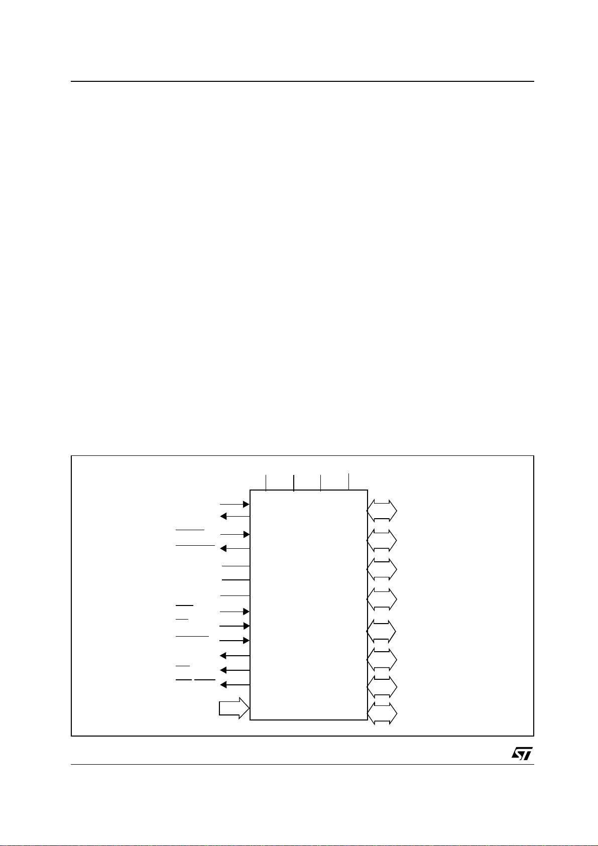
3 - FUNCTIONAL DESCRIPTION
The architecture of the ST10F269Z2 Qx combi nes
advantages of both RISC and CISC processors
and an advanced peripheral subsystem. The
Figure 3 : Block Diagram
ST10F269Z2Qx
block diagram g ives an overview of the different
on-chip components and the high bandwidth
internal bus structure of the ST10F269Z2Qx.
P4.5 C AN1_RXD
P4.6 CAN1_TXD
P4.4 C AN2_RXD
P4.7 CAN2_TXD
256K Byte
Flash Memory
10K Byte
XRAM
CAN1
CAN2
16
Port 0
16
Port 1Port 4
8
Port 6
32 16
CPU-Core and MAC U nit
16
PEC
Interrupt Controller
GPT1
Controller
External Bus
8
10-Bit ADC
GPT2
Port 5
16 15
ASC usart
BRG
Port 3
SSC
BRG
PWM
Port 7
16
16
CAPCOM2
8
2K Byte
Interna l
RAM
Watchdog
Oscillator
and PLL
XTAL1 XTAL2
3.3V Voltage
Regulator
Port 2
CAPCOM1
Port 8
16
8
13/161

ST10F269Z2Qx
4 - MEMORY OR GANIZATION
The memory space of the ST10F269Z2Qx is
configured in a unified memory architecture. Code
memory, data memory, registers and I/O ports are
organized within the same linear address space of
16M Bytes. The entire memory space can be
accessed Byte wise or Word wise. Particular
portions of the on-chip memory have additionally
been made directly bit addressable.
Flash: 256K Bytes of on-chip Flash memory .
IRAM: 2K Bytes of on-chip internal RAM
(dual-port) is provided as a storage for data,
system stack, general purpose registe r b anks and
code. A register bank is 16 Wordwide (R0 to R15)
and / or Bytewide (RL0, RH0, …, RL7, RH7)
general purpose registers.
XRAM: 10K Bytes of on-chip extension RAM
(single port XRAM) is provided as a storage for
data, user stack and code.
The XRAM is divided into 2 areas, the first 2K
Bytes named XRAM1 and the second 8K Bytes
named XRAM2 , connected to the internal XBU S
and are accessed like an external memory in
16-bit demultiplexed bus-mode without wait state
or read/write delay (50ns access at 40MHz CPU
clock). Byte and Word accesses are allowed.
The XRAM1 address range is 00’E000h
- 00’E7FFh if XPEN (bit 2 of SYSCON register),
and XRAM1EN (bit 2 of XPERCON register) are
set. If XRAM1EN or XPEN is cleared, then any
access in the address range 00’E000h
- 00’E7FFh will be directed to external memory
interface, using the BUSCONx register
corresponding to address matching ADDRSELx
register
The XRAM2 address range is 00’C000h
- 00’DFFFh if XPEN (bit 2 of SYSCON register),
and XRAM2 (bit 3 of XPERCON register are set).
If bit XRAM2EN or XPEN is cleared, then any
access in the address range 00’C000h
- 00’DFFFh will be directed to external memory
interface, using the BUSCONx register
corresponding to address matching ADDRSELx
register.
As the XRAM appears like external memory, it
cannot be used as system stack or as register
banks. The XRAM is not provided for single bit
storage and therefore is not bit addressable.
SFR/ESFR: 1024 Bytes (2 x 512 Bytes) of
address space is reserved for the special function
register areas. SFRs are Wordwide registers
which are used to control and to monitor the
function of the different on-chip units.
CAN1: Address range 00’EF00h - 00’EFFFh is
reserved for the CAN1 Module access. The CAN1
is enabled by setting XPEN bit 2 of the SYSCON
register and by setting CAN1EN bit 0 of the new
XPERCON register. Accesses to the CAN Module
use demultiplexed addresses and a 16-bit data
bus (Byte accesses are po ssi b le). T wo wai t states
give an access time of 100ns at 40MHz CPU
clock. No tri-state wait states are used.
CAN2: Address range 00’EE00h - 00’EEFFh is
reserved for the CAN2 Module access. The CAN2
is enabled by setting XPEN bit 2 of the SYSCON
register and by setting CAN2EN bit 1 of the new
XPERCON register. Accesses to the CAN Module
use demultiplexed addresses and a 16-bit data
bus (Byte accesses are po ssi b le). T wo wai t states
give an access time of 100ns at 40MHz CPU
clock. No tri-state wait states are used.
In order to meet the needs of designs where more
memory is required than is provided on chip, up to
16M Bytes of external RAM and/or ROM can be
connected to the microcontroller.
Note If one or the two CAN modules are used,
Port 4 cannot be programmed to output all
8 segment address lines. Thus, only 4
segment address lines can be used,
reducing the external memory space to 5M
Bytes (1M Byte per CS
line).
Visibility of XBUS Peripherals
In order to keep the S T10F269Z2Qx com patible
with the ST10C167 and with the S T10F167, the
XBUS peripherals can be selected to be visible
and / or accessible on the ex t ernal address / dat a
bus. CAN1EN and CAN2EN bits of XPERCON
register must be set. If these bits are cleared
before the global enabling with XPEN-bit in
SYSCON register, the corresponding address
space, port pins and interrupts are not occupied
by the peripheral, thus the peripheral is not visible
and not available. Refe r to Chapter 20 - Special
Function Register Overview.
14/161

Figure 4 : ST10F269Z2Qx On-chip Memory Mapping
14
05’0000
Block6 = 64K Bytes
04’0000
10
Segment 4Segment 3Segment 2Segment 1Segment 0
Block5 = 64K Bytes
0C
03’0000
ST10F269Z2Qx
RAM, SFR and X-pheripherals are
mapped i nt o the addres s space.
00’FFFF
SFR : 512 B yt es
00’FE00
00’FDFF
IRAM : 2K Bytes
00’F600
08
07
06
05
04
03
02
01
00
Data
Page
Number
02’0000
01’8000
01’0000
00’C000
00’6000
00’4000
00’0000
Absolute
Memory
Address
Block4 = 64K Bytes
Block3 = 32K Bytes
Block2*
Block1*
Block0*
Block2 = 8K Bytes
Block1 = 8K Bytes
Block0 = 16K Bytes
Internal
Flash
Memory
Bank 1H
Bank 1L
Bank OL
00’F1FF
ESFR : 51 2 By tes
00’F000
00’EFFF
CAN1 : 256 Bytes
00’EF00
00’EEFF
CAN2 : 256 Bytes
00’EE00
00’EC14
Real Time Clock
00’EC00
00’E7FF
XRAM1 : 2K Bytes
00’E000
00’DFFF
XRAM2 : 8K Bytes
00’C000
* Bank 0L ma y be remapped fr om segment 0 to s egm ent 1 (Bank 1L) by setting SYSCON-R O M S 1 (before EINIT)
Data Page Num ber and Abs ol ute Memory Address are hexadecim al values.
15/161

ST10F269Z2Qx
XPERCON (F024h / 12h) ESFR Reset Value: - - 05h
15 14 13 12 11 10 9 8 7 6 5 4 3 2 1 0
--------
-
CAN1EN CAN1 Enable Bit
‘0’: Accesses to the on-chip CAN1 XPeripheral and its functions are disabled. P4.5 and P4.6 pins can be
used as general purpose I/Os. Address range 00’EF00h-00’EFFFh is only directed to external memory if
CAN2EN is also ‘0’.
‘1’: The on-chip CAN1 XPeripheral is enabled and can be accessed.
CAN2EN CAN2 Enable Bit
‘0’: Accesses to the on-chip CAN2 XPeripheral and its functions are disabled. P4.4 and P4.7 pins can be
used as general purpose I/Os. Address range 00’EE00h-00’EEFFh is only directed to external memory if
CAN1EN is also ‘0’.
‘1’: The on-chip CAN2 XPeripheral is enabled and can be accessed.
XRAM1EN XRAM1 Enable Bit
‘0’: Accesses to external memory within space 00’E000h to 00’E7FFh. The 2K Bytes of internal XRAM1
are disabled.
’1’: Accesses to the internal 2K Bytes of XRAM1.
XRAM2EN XRAM2 Enable Bit
‘0’: Accesses to the external memory within space 00’C000h to 00’DFFFh. The 8K Bytes of internal
XRAM2 are disabled.
’1’: Accesses to the internal 8K Bytes of XRAM2.
RTCEN RTC Enable Bit
’0’: Accesses to the on-chip Real Time Clock are disabled, external access is performed. Address range
00’EC00h-00’ECFFh is only directed to external memory if CAN1EN and CAN2EN are ’0’ also
’1’: The on-chip Real Time Clock is enabled and can be accessed.
--
RTCEN
RW RW RW RW RW
XRAM2EN XRAM1EN CAN2EN CAN1EN
Note: - When both CAN are disabled via XPER-
CON setting, then any access in the
address range 00’EE00h - 00’EFFFh will
be directed to e xternal memory interface,
using the BUSCONx reg ister corresponding to address matching ADDRSELx register. P4.4 and P4.7 can be used as General
Purpose I/O when CAN2 is disabled, and
P4.5 and P4.6 can be used as General
Purpose I/O when CAN1 is disabled.
- The default XPER selection after Reset is
identical to XBUS configuration of
ST10C167: XCAN1 is en abled, XCAN2 is
disabled, XRAM1 (2K Byte compatible
XRAM) is enabled, XRAM 2 (new 8K Byte
XRAM) is disabled.
16/161
- Register XPERCON cannot b e changed
after the global enabling of XPeripherals,
i.e. after the setting of bit XPEN in the
SYSCON register.
- In EMUlation mode, all the XPERipherals
are enabled (XPERCON bit are all set).
The access to external memory and/or
XBus is controlled by the bondout chip.
- When the Real Time Clock is disabled
(RTCEN = 0), the clock oscillator is
switch-off if the ST10 enters in
power-down mode. Otherwise, when the
Real Time Clock is enabled, the bit
RTCOFF of the RTCCON register allows
to choose the power-down mode of the
clock oscillator (See Chapter 16 - Real
Time Clock).

5 - INTERNAL FLASH MEMORY
ST10F269Z2Qx
5.1 - Overview
– 256K Byte on-chip Flash memory
– Two possibilities of Flash mapping into the CPU
address space
– Flash memory can be used for code and data
storage
– 32-bit, zero waitstate read access (50ns cycle
time at f
= 40MHz)
CPU
– Erase-Program Controller (EPC) similar to
M29F400B STM’s stand-alone Flash memo ry
• Word-by-Word Programmable (16µs typica l )
• Data polling and Toggle Protocol for EPC
Status
• Ready/Busy signal connected on XP2INT
interrupt line
• Internal Power-On detection circuit
– Mem ory Erase in blocks
• One 16K Byte, two 8K Byte, one 32K Byte,
three 64K Byte blocks
• Each block can be erased separately
(1.5 second typical)
• Chip erase (8.5 second typical)
• Each block can be separately protected
against programming and erasing
• Each protected block can be temporary unprotected
• When enabled, the read protection prevents
access to data in Flash memory using a program running out of the Flash memory space.
Access to data of internal Flash can only be performed with an inner protected program
– Eras e Susp end and Resum e Modes
• Read and Program another Block during erase
suspend
– Single Voltage operation, no need of dedicated
supply pin
– Low Power Consumption:
• 45mA max. Read current
• 60mA max. Program or Erase current
• Automatic Stand-by-mode (50µA maximum)
– 1000 Erase-Program Cycles per block, 20 years
of data retention time
– Operating temperature: -40 to +125
o
C
5.2 - Operational Overview
Read M ode
In standard mode (the normal operating mode)
the Flash appears like an on-chip ROM with the
same timing and functionality. The Flash module
offers a fast access time, allowing zero w aitstate
access with CPU frequency up to 40MHz.
Instruction fetches and data operand reads are
performed with all addressing modes of the
ST10F269Z2Qx instruction set.
In order to optimize the programming time of the
internal Flash, blocks of 8K Bytes, 16K Bytes,
32K Bytes, 64K Bytes can be used. But the size of
the blocks does not apply to the whole memory
space, see det ails in Table2.
Table 2 : 256K Byte Flash Memory Block Organization
Block Addresses (Segment 0) Addresses (Segment 1) Size (byte)
0
1
2
3
4
5
6
00’0000h to 00’3FFFh
00’4000h to 00’5FFFh
00’6000h to 00’7FFFh
01’8000h to 01’FFFFh
02’0000h to 02’FFFFh
03’0000h to 03’FFFFh
04’0000h to 04’FFFFh
01’0000h to 01’3FFFh
01’4000h to 01’5FFFh
01’6000h to 01’7FFFh
01’8000h to 01’FFFFh
02’0000h to 02’FFFFh
03’0000h to 03’FFFFh
04’0000h to 04’FFFFh
16K
8K
8K
32K
64K
64K
64K
17/161

ST10F269Z2Qx
Instructions and Commands
All operations besides normal read operations are
initiated and controlled by command sequences
written to the Flash Command In terface (CI). The
Command Interface (CI) interprets words written
to the Flash memory and enables one of the
following operations:
– Read memory arr ay
– Program Word
– Block Erase
– Chip Erase
– Erase Suspend
– Erase Resume
– Block Pro tection
– Block Tem porary Unprot ection
– Code Protection
Commands are composed of several write cycles
at specific addresses of the Flash memory. The
different write cycles of such command
sequences offer a fail-safe feature to protect
against an inadvertent write.
A command only starts when the Command
Interface has decoded the last write cycle of an
operation. Until that last write is performed, Flas h
memory remains in Read Mode
Notes: 1. As it is not possible to perform write
operations in the Flash while fetching code
from Flash, the Flash commands must be
written by instructions executed from
internal RAM or external memory.
than one block in parallel. When a time-out period
elapses (96µs) after the last cycle, the
Erase-Program Controller (EPC) automatically
starts and times the erase pulse and executes the
erase operation. There is no need to program the
block to be erased with ‘0000h’ before an erase
operation. Te rmination of operation is indi cated in
the Flash status register. After erase operation,
the Flash memory loca tions are read as 'FFFFh’
value.
Erase Suspend
A block erase operation is typically executed
within 1.5 second for a 64K Byte block. Erasure of
a memory block may be suspended, in order to
read data from another block or to program data in
another block, and then resumed.
In-System Programming
In-system programming is fully supported. No
special programming voltage is required. Because
of the automatic execution of erase and
programming algorithms, write operations are
reduced to transferring commands and data to the
Flash and reading the status. Any code that
programs or erases Flash memo ry locations (that
writes data to the Flash) must be e xecuted from
memory outside th e on-chip Flash memory itself
(on-chip RAM or external memory).
A boot mechanism is provided to support
in-system programming. I t works using seria l link
via USART interface and a PC compatible or
other programming host.
2. Command write cycles d o not need to
be consecutively received, pauses are
allowed, save for Block Erase comm and.
During this operation all Erase Confirm
commands must be sent to complete any
block erase operation before time-out
period expires (typically 96µs). Command
sequencing must be followe d exactly. Any
invalid combination of commands will reset
the Command Interface to Read Mode.
Status R egister
This register is used to flag the status of the
memory and the result of an operation. This
register can be accessed by read cycles during
the Erase-Program Controller (EPC) operation.
Erase Operation
This Flash memory features a block erase
architecture with a chip erase capability too.
Erase is accomplished by executing the six cycle
erase comm and sequence. Additional command
write cycles can then be performed to erase more
18/161
Read/Write Protection
The Flash module supports read and write
protection in a very comfortable and advanced
protection functionality. If Read Protection is
installed, the whole Flash memory is protected
against any "external" read access; read
accesses are only possible with instructions
fetched directly from program Flash memory. For
update of the Flash memory a temporary disable
of Flash Read Protection is supported.
The device als o features a b lock write p rotection.
Software locking of selectable memory blocks is
provided to protect code and data. This feature
will disable both p rogram and erase operations i n
the selected block(s) of the memory. Block
Protection is accomplished by block specific
lock-bit which are programmed by executing a
four cycle command sequence. Th e locked state
of blocks is indicated by specific flags in the
according block status registers. A block may only
be temporarily unlocked for update (write)
operations.

ST10F269Z2Qx
With the two possibilities for write protection whole memory or block specific - a flexible
installation of write protection is supported to
protect the Flash memory or parts of it from
unauthorized programming or erase accesses
and to provide virus-proof protection for all system
code blocks. All write protection also is enabled
during boot operation.
Power Supply, Reset
The Flash module uses a single power supply for
both read and write functions. Internally generated
and regulated voltages are provided for the
program and erase operations from 5V supply.
Once a program or erase cycle has been
completed, the device resets to the standard read
mode. At power-on, the Flash memor y has a setup
phase of some microseconds (dependent on the
power supply ramp-up). During this phase, Flash
can not be read. Thus, if EA
pin is high (execution
will start from Flash memory), the CPU will remains
in reset stat e until the Flas h can be accessed .
5.3 - Architectural Description
The Flash module distinguishes two basic
operating modes, the standard read mode and the
command mode . The initial state after power-on
and after reset is the standard read mode.
5.3.1 - Read Mode
The Flash module enters the standard operating
mode, the read mode:
– After Reset command
– After every completed erase operat ion
– After every completed program m ing operation
– After every other completed command
execution
– Few microseconds after a CPU-reset has
started
– After incorrect address and data values of
command sequences or writing them in an
improper sequence
– After incorrect write access to a read protect ed
Flash memory
The read mode remains active until the last
command of a command sequence is decoded
which starts directly a Flash array operation, such
as:
– erase one or several blocks
– program a word into Flash array
– protect / temporary unprotect a block.
In the standard read mode read accesses are
directly controlled by the Flash memory array,
delivering a 32-bit double Word from the
addressed position. Read accesses are always
aligned to double Word boundaries. Thus, both
low order address bit A1 and A0 are not used in
the Flash array for read accesses. T he high order
address bit A17/A16 define t he ph ysical 64K Byte
segment being accessed within the Flash array.
5.3.2 - Command Mode
Every operation besides standard read operations
is initiated by commands written to the Flash
command register. The addresses used for
command cycles define in conjunction with the
actual state the specific step within command
sequences. With the last command of a command
sequence, the Erase-Program Controller (EPC)
starts the execution of the command. The EPC
status is indicated during command execution by:
– The Status Register,
– The Ready / Busy signal .
5.3.3 - Ready/Busy Signal
The Ready/Busy (R
XPER2 interr u p t node (XP2IC). When R
/B) signal is connected to the
/B is high,
the Flash is busy with a Program or Erase
operation and will not accept any additional
program or erase instruction. When R
/B is Low,
the Flash is ready for any Read/Write or Erase
operation. The R
/B will also be low when the
memory is put in Erase Suspend mode.
This signal can be polled by reading XP2IC
register, or can be used to trigger an interrupt
when the Flash goes from Busy to Ready.
5.3.4 - Flash Status Register
The Flash Status register is used to flag the status
of the Flash memory and the result of an
operation. This register can be accessed by Read
cycles during the program-Erase Controller
operations. The program or erase operation can
be controlled by data polling on bit FSB.7 of
Status Register, detection of Toggle on FSB.6 and
FSB.2, or Error on FSB.5 and Erase Time-out on
FSB.3 bit. Any rea d attempt in Flas h during EPC
operation will au tomatically out put these five b its.
The EPC sets bit FSB.2, FSB.3, FSB.5, FSB.6
and FSB.7. Other bits are res erved for future us e
and should be masked.
19/161

ST10F269Z2Qx
Flash Status (see note for address)
15 14 13 12 11 10 9 8 7 6 5 4 3 2 1 0
-------- FSB.7 FSB.6 FSB.5 - FSB.3 FSB.2 - RRR RR
FSB.7 Flash Status bit 7: Data Polling Bit
Programming Operation: this bit outputs the complement of the bit 7 of the word being
programmed, and after completion, will output the bit 7 of the word programmed.
Erasing Operation: outputs a ‘0’ during erasing, and ‘1’ after erasing completion.
If the block selected for erasure is (are) protected, FSB.7 will be set to ‘0’ for about 100 µs, and
then return to the previous addressed memory data value.
FSB.7 will also flag the Erase Suspend Mode by switching from ‘0’ to ‘1’ at the start of the
Erase Suspend.
During Program operation in Erase Suspend Mode, FSB.7 will have the same behaviour as in
normal Program execution outside the Suspend mode.
FSB.6 Fl as h S ta tus bi t 6: Toggle Bit
Programming or Erasing Operat ions: success ive read operation s of Flash S tatus register will
deliver complementary values. FSB.6 will toggle each time the F lash Status register is read .
The Program operation is comp leted when two successive reads yield the same value. The
next read will output the bit last programmed, or a ‘1’ after Erase operation
FSB.6 will be set to‘1’ if a read operation is attempted on an Erase Suspended block. In
addition, an Erase Suspend/Resume command will cause FSB. 6 to toggle.
FSB.5 Flash Status bit 5: Erro r Bit
This bit is set to ‘1’ when there is a failure of Program, block or chip erase operations.This bit
will also be set if a user tries to program a bit to ‘1’ to a Flash location that is currently
programmed with ‘0’.
The error bit resets after Read/Reset instruction.
In case of s u c c es s, the Error bit will be s et to ‘0’ duri ng P ro gr am or Erase a nd then w ill output
the bit last programmed or a ‘1’ after erasing
FSB.3 Flash Status bit 3: Erase Time-out Bit
This bit is cleared by the EPC when the last B lock Erase command has been entered to the
Command Interface and it is awaiting the E rase start. When the tim e-out period is finished,
after 96 µs, FSB.3 returns back to ‘1’.
FSB.2 Fl as h S ta tus bi t 2: Toggle Bit
This toggle bit, together with FSB.6, can be used to determine the chip status during the Erase
Mode or Erase Suspend Mode. It can be used also to identify the block being Erased
Suspended. A Read operation will cause FSB.2 to Toggle during the Erase Mode. If the Flash
is in Erase Suspend Mode, a Read operation from the Erase suspended block or a Program
operation into the Erase suspended block will c ause FS B .2 to toggle.
When the Flash is in Program Mode during Erase Suspend, FSB.2 will be read as ‘1’ if address
used is the address of the word being programmed.
After Erase completion with an Error status, FSB.2 will toggle when reading the faulty sector.
Note: The Address of Flash Status Register is the address of the word being programmed when
Programming operation is in progress, or an address within block being erased when Erasing
operation is in progress.
20/161

ST10F269Z2Qx
5.3.5 - Flash Protection Register
The Flash Protection regis ter is a non-volatile register that contains the protection status. This register
can be read by using the Read Protection Status (RP ) command, and programmed by using the dedicated Set Protection command.
Flash Protection Register (PR)
1514131211109876543 2 10
CP------ - -BP6BP5BP4BP3BP2BP1BP0
BPx Block x Protection Bit (x = 0...6)
‘0’: the Block Protection is enabled for block x. Programming or erasing the block is not
possible, unless a Block Temporary Unprotection command is issued.
1’: the Block Protection is disabled for block x.
Bit is ‘1’ by default, and can be programmed permanently to ‘0’ using the Set Protection
command but then cannot be set to ‘1’ again. It is therefore possible to temporally disable the
Block Protection using the Block Temporary Unprotection instruction.
CP Code Protection Bit
‘0’: the Flash Code Protection is enabled. Read accesses to the Flash for execution not
performed in the Flash itself are not allowed, the returned value will be 009Bh, whatever the
content of the Flash is.
1’: the Flash Code Protection is disabled: read accesses to the Flash from external or internal
RAM are allowed
Bit is ‘1’ by default, and can be programmed permanently to ‘0’ using the Set Protection
command but then cannot be set to ‘1’ again. It is therefore possible to temporally disable the
Code Protection using the Code Temporary Unprotection instruction.
5.3.6 - Instructions Description
Twelve instructions dedicated to Flash memory
accesses are defined as follow:
Read/Reset (RD). The Read/Reset instruction
consist of one write cycle with data XXF0h. it can
be optionally preceded by two CI enable
coded
cycles (data xxA8h at address 1554h + data
xx54h at address 2AA8h). Any successive read
cycle following a Read/Reset instruction will read
the memory array. A Wait cycle of 10µs is
necessary after a Read/Reset command if the
memory was in program or Erase mode.
Program Word (PW). This instruction uses four
write cycles. After the two Cl enable coded cycles,
the Program Word comm and xxA0h is written at
address 1554h. The following write cycle will latch
the address and data of the word to be
programmed. Memory programming can be do ne
only by writing 0's instead of 1's, otherwise an
error occurs. During programming, the Flash
Status is che cked by rea ding the F lash Statu s bit
FSB.2, FSB.5, FSB.6 and F SB.7 which show the
status of the EPC. FSB.2, FSB.6 and FSB.7
determine if programming is on going or has
completed, and FSB.5 allows a check to be made
for any possible error.
Block Erase (BE). This instruction uses a
minimum of six command cycles. The erase
enable command xx80h is written at address
1554h after the two-cycle CI enable sequence.
The erase confirm code xx30h must be written at
an address related to the block to be erased
preceded by the execution of a second CI enable
sequence. Additional erase confirm codes must
be given to erase m ore t han one block in parallel.
Additional erase confirm commands must be
written within a defined time-out period. The input
of a new Block Erase command will restart the
time-out period.
When this time-out period has elapsed, the erase
starts. The status of the internal timer can be
monitored through the level of FSB.3, if FSB.3 is
‘0’, the Block Erase command has been given and
the time-out is running; if FSB.3 is ‘1’, the time-out
has expired and the EPC is erasing the block(s).
21/161

ST10F269Z2Qx
If the second command given is not an erase
confirm or if the coded cycles are wrong, the
instruction aborts, and the device is reset to Read
Mode. It is not necessar y to progr am the bloc k with
0000h as the EPC will do this automatically before
the erasing to FFFFh. Read operations after the
EPC has started, output the Flash Status Register .
During the execution of the erase by the EPC, the
device accepts only the Erase Suspend and
Read/Reset instructions. Data Polling bit FSB.7
returns ‘0’ while the erasure is in progress, and ‘1’
when it has completed. The Toggle bit FSB.2 and
FSB.6 toggle during the erase operation. They
stop when era se is completed. After completion,
the Error bit FSB.5 returns ‘1’ if there has been an
erase failure because erasure has not completed
even after the maximum number of erase cycles
have been execut ed by the EPC, in this case, it
will be necessary to input a Read/Reset to the
Command Interface in order to reset the EPC.
Chip Erase (CE). This instruction uses six write
cycles. The Erase Enable command xx80h, must
be written at address 1554h after CI-Enable
cycles. The Chip Erase command xx10h must be
given on the sixth cycle after a second CI-Enable
sequence. An error in command sequence will
reset the CI to Read mode. It is NOT necessary to
program the block with 0000h as the EPC will do
this automatically before the erasing to FFFFh.
Read operations after the EPC h as started out put
the Flash Status Register. During the execution of
the erase by the EPC, Data Polling bit FSB.7
returns ‘0’ while the erasure is in progress, and ‘1’
when it has completed. The FSB.2 and FSB.6 bit
toggle during the erase operation. They stop
when erase is finished. The FSB.5 error bit
returns "1" in case of failure of the erase
operation. The error flag is set after the maxim um
number of erase cycles have been executed by
the EPC. In this case, it will be neces sary to input
a Read/Reset to the Command Interface in order
to re s e t the EP C .
Erase Suspend (ES). This instruction can be
used to suspend a Block Erase operation by
giving the command xxB0h without any specific
address. No CI-Enable cycles is required. Erase
Suspend operation allows reading of data from
another block and/or the programming in another
block while erase is in progress. If this com mand
is given during the time-out period, it will terminate
the time-out period in additi on to erase Suspend.
The Toggle bit FSB.6, when monitored at an
address that belon gs to the block being erased,
stops toggling when E ras e Sus pend Com m and is
effective, It happens between 0.1µs and 15µs
after the Erase Suspend Command has been
written. The Flash will then go in normal Read
Mode, and read from b locks not being erased is
valid, while read from block being erased will
output FSB.2 toggling. During a Suspend p hase
the only instructions valid are Erase Resum e and
Program Word. A Read / Reset instruction during
Erase suspend will definitely abort the Erase and
result in invalid data in the block being erased.
Erase Resume (ER). This instruction can be
given when the memory is in Erase Suspend
State. Erase can be resumed by writing the
command xx30h at any address without any
Cl-enable sequence.
Program d uring Erase Suspend. The Program
Word instruction during Erase Suspend is allowed
only on blocks that are not Erase-suspended. This
instruction is the same than the Program Word
instruction.
Set Protection (SP). This instruction can be used
to enable both Block Protection (to protect each
block independ ently from accidental E rasing-Programming Operation) and Code Protection (to
avoid code dump). The Set Protection Com mand
must be given after a special CI-Protection Enable
cycles (see instruction table). The following Write
cycle, will program the Protection Register. To
protect the block x (x = 0 to 6), the data bit x must
be at ‘0’. To p ro tect the code, bit 15 of the data
must be ‘0’. Enabling Block or Code Protection is
permanent and can be cleared only by STM.
Block Temp orary Unprotection and Code Temporary Unprotection instructions are available to
allow the customer to update the code.
Notes: 1. The new val ue programme d i n protecti on
register w ill on ly beco m e activ e a fte r a re set.
2. Bit that are already at ’0’ in protec tion
register must be confirmed at ’0’ also in
data latched during the 4th cycle of set
protection command, otherwise an error
may occur.
Read Protection Status (RP). T his inst ruction is
used to read the Blo ck Protection status and the
Code Protection status. To read the protection
register (see Table 3), the CI-Protection Enable
cycles must be executed followed by the
command xx90h at address x2A54h. The
following Read Cycles at any odd wo rd address
will output the Block Protection Status. The Read/
Reset command xxF0h must b e written to reset
the protection interface.
Note: After a modification of protection register
(using Set Protection command), the Read
22/161

ST10F269Z2Qx
Protection Status will return the new PR
value only after a reset.
Block Temporary Unprotection (BTU). This Instruction can be used to temporary unprotect all the
blocks from Program / Erase prot ection. The Unprotection is disabled after a Reset cycle. The Block
Temporary Un protection comman d xxC1h must be given to enable B lock Tem porary Unprotection. The
Command must be preceded by the CI-Protection Enable cycles and followed by the Read/Reset
command xxF0h.
Set Code Protection (SCP). This kind of protection allows the customer to protect the proprietary code
written in Flash. If installed and active, Flash Code Protection prevents data operand accesses and
program branches into the on-chi p Flash area from any location outside the Flash memory it self. Data
operand accesses and branches to Flash locations are only and exclusively allowed for instructions
executed from the Flash memory itself. Every read or jump to Flash performed from another memory (like
internal RAM, external m emory) wh ile Code P rot ection is en abled, wi ll giv e the opc od e 009B h related to
TRAP #00 illegal instruction. The CI-Protection Enable cycles must be sent to set the Code Protection. By
writing data 7FFFh at any odd word add ress, the Code P rotected s tatus is sto red in the Flash Pr otec tion
Register (PR). Protection is permanent and cannot be cleared by the user. It is possible to temporarily
disable the Code Protection using Code Temp orary Unprotection instruction .
Note: Bits that are already at ’0’ in protection register must be confirmed at ’0’ also in data latched during
the 4th cycle of set protection command, otherwise an error may occur.
Code Temporary Unprotection (CTU). This instruction must be used to temporary disable Code
Protection. This instruction is effective only if executed from Flash memory space. To restore the
protection status, without using a reset, it is necessary to use a Code Temporary Protection instruction.
System reset will res et also the Code Temporary Unprotected status. The Code Temporary Unprotection
command consists of the following write cycle:
MOV MEM, Rn ; This instruction MUST be executed from Flash memory space
Where MEM is an absolute address inside memory space, Rn is a register loaded with data 0FFFFh.
Code Temporary Protection (CTP). This instruction allows to restore Code Protection. This operation is
effective only if ex ecuted from Flash m emory an d is nec essary to res tore the protection st atus after the
use of a Code Temporary Unprotection instruction.
The Code Tem porary Protection command consists of the following write cycle:
MOV MEM, Rn ; This instruction MUST be executed from Flash memory space
Where MEM is an absolute address inside memory space, Rn is a register loaded with data 0FFFBh.
Note that Code Temporary Unprotection instruction must be used when it is necessary to modify the
Flash with protected code (SCP), since the write/erase routines must be executed from a memory
external to Flash space. Usually, the write/erase routines, executed in RAM, ends with a return to Flash
space where a CTP instruction restore the protection.
23/161

ST10F269Z2Qx
Table 3 : Instructions
Instruction Mne Cycle
Read/Reset RD 1+
Addr.
st
1
Cycle
1
X
2
nd
2
Cycle
3rd
Cycle
th
4
Cycle
th
5
Cycle
6th
Cycle
Read Memory Array until a new write cycle is initiated
Data xxF0h
1
Read/Reset RD 3+
Program Word PW 4
Block Erase BE 6
Addr.
Data xxA8h xx54h xxF0h
Addr.
Data xxA8h xx54h xxA0h
Addr.
x1554h x2AA8h xxxxxh
Read Memory Array until a new write
cycle is initiated
1
x1554h x2AA8h x1554h
1
x1554h x2AA8h x1554h x1554h x2AA8h BA
WA
WD
3
Read Data Polling or Toggle
bit until Program completes.
4
Data xxA8h xx54h xx80h xxA8h xx54h xx30h xx30h
1
Chip Erase CE 6
Addr.
x1554h x2AA 8h x1554h x1554h x2AA8h x15 54h
Data xxA8h xx5 4h xx80h xxA8h xx54h xx10h
1
Erase Suspend ES 1
Addr.
Data xxB0h
1
Erase Resume ER 1
Addr.
Data xx30h
Set Block/Code
Protection
Addr.
1
SP 4
Data xxA8h xx54h xxC0h
Read
Protection
Status
RP 4
Addr.
1
Data xxA8h xx5 4h xx90h R ead PR
Block
Temp orary
BTU 4
Unprotection
Code
Temp orary
CTU 1
Unprotection
Code
Temporary
CTP 1
Protection
Notes 1. Address bit A14, A15 and above are don’t care for coded address inputs.
2. X = Don’t Care.
3. WA = Write Address: address of memory location to be programmed.
4. WD = Write Data: 16-bit data to be programmed
5. Optional , addition al bl ocks addre ss es must be ent ered within a time-out del ay (96 µs) after last writ e entry, time-out sta tus can be
verified through FSB.3 value. When full command is entered, read Data Polling or Toggle bit until Erase is completed or suspended.
6. Read Da ta Polling or Toggle bit unt i l Erase compl etes.
7. WPR = Wr i te protecti on register. To protect c ode, bit 15 of WPR must be ‘0’. To protect block N (N =0,1,...), bit N of WPR m u st be
‘0’. Bit that are already at ‘0’ in protection register must also be ‘0’ in WPR, else a writing error will occurs (it is not possible to write a
‘1’ in a bit already programmed at ‘0’).
8. MEM = any add ress insid e the Fl ash m emor y space. Abso lut e addre ssi ng mo de mus t be us ed (MO V MEM, Rn), an d instru cti on
must be executed from Flash memory space.
9. Odd word address = 4n-2 w here n = 0, 1, 2, 3..., ex. 0002h, 0006h...
1
Addr.
Data xxA8h xx5 4h xxC1h xxF0h
1
Addr.
Data FFFFh
1
Addr.
Data FFFBh
2
X
Read until Toggle stops, then read or program all data needed
from block(s) not being erased then Resume Erase.
2
X
Read Data Polling or Toggle bit until Erase completes or Erase is
suspended anoth er time.
x2A54h x15A8h x2A54h Any odd
word
address
7
WPR
x2A54h x15A8h x2A54h Any odd
word
address
x2A54h x15A 8h x2A54h
8
MEM
MEM
Write cycles must be executed from Flash.
8
Write cycles must be executed from Flash.
2
X
9
Read Protection Register
9
until a new write cycle is
initiated.
7th
Cycle
BA’
Note
5
6
24/161

ST10F269Z2Qx
– Generally, command sequences cannot be
written to Flash by instructions fetched from the
Flash itself. Thus, the Flash commands must be
written by instructions, executed from internal
RAM or external memory.
– Command cycles on the CPU interface need not
to be consecutively recei ved (pauses allowed).
The CPU interface delivers dummy read data for
not used cycles within command sequences.
– All addresses of command cycles shall be
defined only with Register-indirect addressing
mode in the according move instructi o ns. Di re ct
addressing is not allowed for command
sequences. Address segment or data page
pointer are taken into account for the com mand
address value.
5.3.7 - Reset Processing and Initial State
The Flash module distinguishes two kinds of CPU
reset types
The lengthening of CPU reset:
– Is not reported to external devices by
bidirectional pin
– Is not enabled in case of external start of CPU
after reset.
5.4 - Flash Memory Configuration
The default memory configuration of the
ST10F269Z2Qx Memory is determined by the
state of the EA
pin at reset. This value is stored in
the Internal ROM Enable bit (named ROMEN) of
the SYSCON register.
When ROMEN = 0, the internal Flas h is disabled
and external ROM is used for startup control.
Flash memory can later be enabled by setting the
ROMEN bit of SYSCON to 1. The code
performing this setting must not run from a
segment of the e xternal ROM to be replaced by a
segment of the Flash memory, otherwise
unexpected behaviour may occur.
For example, if external ROM code is located in
the first 32K Bytes of segment 0, the first
32K Bytes of the Flash must then be enabled in
segment 1. This is done by setting the ROMS1 bit
of SYSCON to 0 before or simultaneously with
setting of ROMEN bit. This must be done in the
externally supplied program before t he execution
of th e EINI T instruction.
If program execution starts from external memory,
but access to the Flash memory mapped in
segment 0 is later required, then the code that
performs the setting of ROMEN bit must be
executed either in the segment 0 but above
address 00’8000h, or from the internal RAM.
Bit ROMS1 only affects the mapping of the first
32K Bytes of the Fla sh memory. All other parts of
the Flash memory (addresses 01’8000h 04’FFFFh) remain unaffected.
The SGTDIS Segmentation Disable / Enable must
also be set to 0 to allow the use of the full
256K Bytes of on-chip memory in addi tion to the
external boot memory. The correct procedure on
changing the segmentation registers must also be
observed to prevent an unwanted trap condition:
– Instructions that configure the internal memory
must only be executed from external memory or
from the internal RAM.
– An Absolute Inter-Segment Jump (JMPS)
instruction must be executed after Flash
enabling, to the next instruction, even if this next
instruction is located in the consecutive address.
– Whenever the internal Memory is disabled,
enabled or remapped, the DPPs must be
explicitly (re)loaded to enable correct data
accesses to the internal memory and/or external
memory.
5.5 - Application Examples
5.5.1 - Handling of Flash Addresses
All command, Block, Data and register addresses
to the Flash have to be located within the active
Flash memory space. The active space is that
address range to which the physical Flash
addresses are mapped as defined by the user.
When using data page pointer (DPP) for block
addresses make sure that address bit A15 and
A14 of the block address are reflected in both
LSBs of the selected DPPS.
Note: - For Command Instructions, address bit
A14, A15, A16 and A17 are don’t care.
This simplify a lot the applicati on software,
because it minimize the use o f DPP registers when using Command in the Command Interface.
- Direct addressing is not allowed for
Command sequence operations to the
Flash. Only Register-indirect addressing
can be used for command, block or
write-data accesses.
25/161

ST10F269Z2Qx
5.5.2 - Basic Flash Access Control
When accessing the Flash all command write addresses have to be located within the active Flash
memory space. Th e active Flash memory space is that logical address range which is covered by the
Flash after m apping. When usin g data page pointer (DPP) for addressing the Flash, make sure that
address bit A15 and A14 of the command addresses are reflected in both LSBs of the selected data page
pointer (A15 - DPPx.1 and A14 - DPPx.0).
In case of the command write addresses, address bit A14, A15 and above are don’t care. Thus,
command writes can be performed by only using one DPP register. This allow to have a more simple and
compact application software.
Another - advantageous - possibility is to use the extended segment instruction for addressing.
Note: The direct addressing mode is not allowed for write access to the Flash address/command
register. Be aware that the C compiler may use this kind of addressing. For write accesses to
Flash module always the indirect addressing mode has to be selected.
The following basic instruction sequences show examples for different addressing possibilities.
Principle example of address gene ration for Flash commands and registers:
When using data page pointer (DPP0 is this example)
MOV DPP0,#08h ;adjust data page pointers according to the
;addresses: DPP0 is used in this example, thus
;ADDRESS must have A14 and A15 bit set to ‘0’.
MOV Rw
,#ADDRESS ;ADDRESS could be a dedicated command sequence
m
;address 2AA8h, 1554h ... ) or the Flash write
;address
MOV Rw
,#DATA ;DATA could be a dedicated command sequence data
n
;(xxA0h,xx80h ... ) or data to be programmed
MOV [Rw
],Rw
m
n
;indirect addressing
When using the extended segment instruction:
MOV Rw
,#ADDRESS ;ADDRESS could be a dedicated command sequence
m
;address (2AA8h, 1554h ... ) or the Flash write
;address
MOV Rw
,#DATA ;DATA could be a dedicated command sequence data
o
;(xxA0h,xx80h ... ) or data to be programmed
MOV Rw
,#SEGMENT ;the value of SEGMENT represents the segment
n
;number and could be 0, 1, 2, 3 or 4 (depending
;on sector mapping) for 256KByte Flash.
EXTS Rw
,#LENGTH ;the value of Rwn determines the 8-bit segment
n
;valid for the corresponding data access for any
;long or indirect address in the following(s)
;instruction(s). LENGTH defines the number of
;the effected instruction(s) and has to be a value
;between 1...4
MOV [Rw
26/161
],Rw
m
o
;indirect addressing with segment number from
;EXTS

ST10F269Z2Qx
5.5.3 - Programming Exampl es
Most of the microcontro ller programs are written in the C language where t he data page pointers are
automatically set by the compiler. But because the C compiler may use the not allowed direct addressing
mode for Flash write addresses, it is necessary to program the organizational Flash accesses (command
sequences) with assembler in-line routines which use indirect addressing.
Example 1 Performing the command Read/Reset
We assume that in the initialization phase the lowe st 32K Bytes of Flash memory (sector 0) have be en
mapped to segment 1.
According to the usual way of ST10 data addressing with data page pointers, address bit A15 and A14 of
a 16-bit command write address sel ect the dat a page poi nter (DPP) which cont ains the uppe r 10-bit for
building the 24-bit physical data address. Ad dress bit A13...A0 represent the address offset. As the bit
A14...A17 are "don’t care" when written a Flash command in the Command Interface (CI), we can choose
the most convenient DPPx register for address handling.
The following examples are m aking usage of DPP0. We just have to make su re, that DPP0 points to
active Flash memory space.
To be independent of mapping of s ector 0 we choose for all DPPs which are used for Flash address
handling, to point to segment 2.
For this reason we load DPP0 with value 08h (00 0000 l000b).
MOV R5, #01554h ;load auxilary register R5 with command address
;(used in command cycle 1)
MOV R6, #02AA8h ;load auxilary register R6 with command address
;(used in command cycle 2)
SCXT DPPO, #08h ;push data page pointer 0 and load it to point to
;segment 2
MOV R7, #0A8h ;load register R7 with 1st CI enable command
MOV [R5], R7 ;command cycle 1
MOV R7, #054h ;load register R7 with 2cd CI enable command
MOV [R6], R7 ;command cycle 2
MOV R7, #0F0h ;load register R7 with Read/Reset command
MOV [R5], R7 ;command cycle 3. Address is don’t care
POP DPP0 ;restore DPP0 value
In the example above the 16-bit registers R5 and R6 are used as auxiliary registers for indirect
addressing.
Example 2 Performing a Program Word command
We assume that in the initialization phase the lowe st 32K Bytes of Flash memory (sector 0) have be en
mapped to segment 1.Th e data to be written is loaded in register R13, the addres s to be program me d is
loaded in register R11/R12 (segment number in R11, segment offset in R12).
MOV R5, #01554h ;load auxilary register R5 with command address
;(used in command cycle 1)
MOV R6, #02AA8h ;load auxilary register R6 with command address
;(used in command cycle 2)
SXCT DPPO, #08h ;push data page pointer 0 and load it to point to
;segment 2
MOV R7, #0A8h ;load register R7 with 1st CI enable command
MOV [R5], R7 ;command cycle 1
MOV R7, #054h ;load register R7 with 2cd CI enable command
MOV [R6], R7 ;command cycle 2
MOV R7, #0A0h ;load register R7 with Program Word command
MOV [R5], R7 ;command cycle 3
27/161

ST10F269Z2Qx
POP DPP0 ;restore DPP0: following addressing to the Flash
;will use EXTended instructions
;R11 contains the segment to be programmed
;R12 contains the segment offset address to be
;programmed
;R13 contains the data to be programmed
EXTS R11, #1 ;use EXTended addressing for next MOV instruction
MOV [R12], R13 ;command cycle 4: the EPC starts execution of
;Programming Command
Data_Polling:
EXTS R11, #1 ;use EXTended addressing for next MOV instruction
MOV R7, [R12] ;read Flash Status register (FSB) in R7
MOV R6, R7 ;save it in R6 register
;Check if FSB.7 = Data.7 (i.e. R7.7 = R13.7)
XOR R7, R13
JNB R7.7, Prog_OK
;Check if FSB.5 = 1 (Programming Error)
JNB R6.5, Data_Polling
;Programming Error: verify is Flash programmed
;data is OK
EXTS R11, #1 ;use EXTended addressing for next MOV instruction
MOV R7, [R12] ;read Flash Status register (FSB) in R7
;Check if FSB.7 = Data.7
XOR R7, R13
JNB R7.7, Prog_OK
;Programming failed: Flash remains in Write
;Operation.
;To go back to normal Read operations, a Read/Reset
;command
;must be performed
Prog_Error:
MOV R7, #0F0h ;load register R7 with Read/Reset command
EXTS R11, #1 ;use EXTended addressing for next MOV instruction
MOV [R12], R7 ;address is don’t care for Read/Reset command
... ;here place specific Error handling code
...
...
;When programming operation finished succesfully,
;Flash is set back automatically to normal Read Mode
Prog_OK:
....
....
28/161

ST10F269Z2Qx
Example 3 Performing the Block Erase command
We assume that in the initialization phase the lowe st 32K Bytes of Flash memory (sector 0) have be en
mapped to segment 1.The registers R11/R12 contain an address related to the block to be erased
(segment number in R11, segment offset in R12, for example R1 1 = 01h, R12= 4000h will erase the block
1 - first 8K byte block).
MOV R5, #01554h ;load auxilary register R5 with command address
;(used in command cycle 1)
MOV R6, #02AA8h ;load auxilary register R6 with command address
;(used in command cycle 2)
SXCT DPPO, #08h ;push data page pointer 0 and load it to point ;to
;segment 2
MOV R7, #0A8h ;load register R7 with 1st CI enable command
MOV [R5], R7 ;command cycle 1
MOV R7, #054h ;load register R7 with 2cd CI enable command
MOV [R6], R7 ;command cycle 2
MOV R7, #080h ;load register R7 with Block Erase command
MOV [R5], R7 ;command cycle 3
MOV R7, #0A8h ;load register R7 with 1st CI enable command
MOV [R5], R7 ;command cycle 4
MOV R7, #054h ;load register R7 with 2cd CI enable command
MOV [R6], R7 ;command cycle 5
POP DPP0 ;restore DPP0: following addressing to the Flash
;will use EXTended instructions
;R11 contains the segment of the block to be erased
;R12 contains the segment offset address of the
;block to be erased
MOV R7, #030h ;load register R7 with erase confirm code
EXTS R11, #1 ;use EXTended addressing for next MOV instruction
MOV [R12], R7 ;command cycle 6: the EPC starts execution of
;Erasing Command
Erase_Polling:
EXTS R11, #1 ;use EXTended addressing for next MOV instruction
MOV R7, [R12] ;read Flash Status register (FSB) in R7
;Check if FSB.7 = ‘1’ (i.e. R7.7 = ‘1’)
JB R7.7, Erase_OK
;Check if FSB.5 = 1 (Erasing Error)
JNB R7.5, Erase_Polling
;Programming failed: Flash remains in Write
;Operation.
;To go back to normal Read operations, a Read/Reset
;command
;must be performed
Erase_Error:
MOV R7, #0F0h ;load register R7 with Read/Reset command
EXTS R11, #1 ;use EXTended addressing for next MOV instruction
MOV [R12], R7 ;address is don’t care for Read/Reset command
... ;here place specific Error handling code
...
...
;When erasing operation finished succesfully,
;Flash is set back automatically to normal Read Mode
Erase_OK:
....
....
29/161
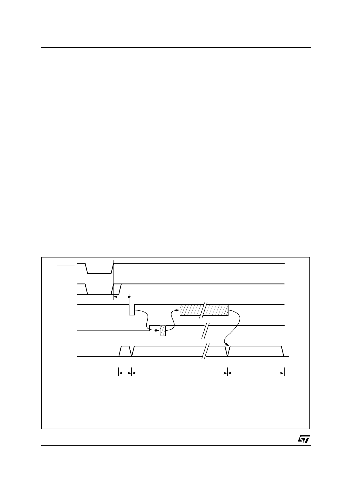
ST10F269Z2Qx
5.6 - Bootstrap Loader
The built-in bootstrap loader (BSL) of the
ST10F269Z2Qx provides a mechanism to load
the startup program through the serial interface
after reset. In this case, no external memory or
internal Flash memory is required for the
initialization code starting at location 00’0000h
(see Figure 5).
The bootstrap loader moves code/data into the
internal RAM, but can also transfer data via the
serial interface into an external RAM using a
second level loader routine. Flash Memory
(internal or external) is not ne cessary, but it may
be used to provide lookup tables or “core-code”
like a set of general purpose subroutines for I/O
operations, number crunching, system
initiali zat io n, etc.
The bootstrap loader can be used to load the
complete application software into ROMless
systems, to load temporary software into
complete systems for testing or calibration, or to
load a programming routine for Flash devices.
The BSL mechanism can be used for standard
system startup as well as for special occasions
like system maintenance (firmer update) or
end-of-line programming or testing.
5.6.1 - Entering the Bootstrap Loader
The ST10F269Z2Qx ent ers BSL mode when pin
P0L.4 is sampled low at the end of a hardware
reset. In this case the built-in bootstrap loader is
activated independent of the selected bus mode.
The bootstrap loader code is stored in a special
Boot-ROM. No part of the standard mask Memory
or Flash Memory area is required for this.
After entering BSL mode and the respective
initialization the ST10F269Z2Qx scans the RX D0
line to receive a zero Byte, one start bit, eight ‘0’
data bits and one stop bit.
From the d uration of this zero B yte it calculates
the corresponding Baud rate factor with respect to
the current CPU clock, initializes the serial
interface ASC0 accordingly and switches pin
TxD0 to output.
Using this Baud rate, an identification Byte is
returned to the host that provides the loaded data.
This identification Byte identifies the device to
be booted. The identification byte is D5h for
ST10F269Z2Qx.
Figure 5 : Bootstrap Loader Sequence
RSTIN
P0L.4
1)
2)
RxD0
3)
TxD0
5)
CSP:IP
Internal Boot Memory (BSL) routine 32 Byte user software
6)
1) BSL initialization time
2) Zero Byte (1 start bit, eight ‘0’ data bits, 1 stop bit), sent by host.
3) Identifica tion Byte (D5h), sent by ST10F269Z2Qx.
4) 32 Byte s of code / data, se nt by host.
5) Caution: TxD0 is only driven a certain time after reception of the zero Byte.
6) Internal Bo ot ROM.
4)
30/161

ST10F269Z2Qx
When the ST10F269Z2Qx has entered BSL mode, the following configuration is automatically set (values
that deviate from the normal reset values, are
marked
):
Watchdog Timer:
Context Pointer CP: FA00h Register STKUN: FA40h
Stack Pointer SP: FA40h Register STKOV: FA0Ch 0<->C
Register S0CON:
Register S0BG: Acc. to ‘00’ Byte
In this case, the watchdog timer is disabled, so the
Disabled
8011h
Register BUSCON0: acc. to startup configuration
Register SYSCON: 0E00h
P3.10 / TXD0: ‘1’
DP3.10: ‘1’
5.6.2 - Memory Configuration After Reset
bootstrap loading sequence is not time limited.
The configuration (and the accessibility) of the
Pin TXD0 is configured as output, so the
ST10F269Z2Qx can return the identification Byte.
Even if the internal Flash is enabled, no code can
be executed out of it.
The hardware that activates the BSL d uring reset
may be a simple pul l-down resistor on P0L.4 for
systems that use this feature upon every
hardware reset.
A switchable solution (via jumper or an external
signal) can be used for systems that
only temporarily use the bootstrap loader (see
Figure 6).
After sending the identification Byte the
ASC0 receiver is enabled and is ready to
receive the initial 32 Bytes fr om the host. A half
duplex connection is therefore sufficient to feed
the BSL.
ST10F269Z2Qx’s memory areas after reset in
Bootstrap-Loader mode differs from the standard
case. Pin EA
is not evaluated when B SL mode is
selected, and accesses t o the internal Flash a rea
are partly redirected, while the ST10F269Z2Qx is
in BSL mod e (see Fig ure 7). All code fetches are
made from the special Boot-ROM, while data
accesses read from the internal u ser Flash. Data
accesses will return undefined values on
ROMless devices.
The code in the Boot-ROM is not an invariant
feature of the ST10F269Z2Qx. User software
should not try to execute code from the internal
Flash area while the BSL m ode is still active, as
these fetches will be redirected to the Boot-ROM.
The Boot-ROM will also “move” to segment 1,
when the internal Flash area is mapped to
segment 1 (see Figure 7).
Figure 6 : Hardware Provisions to Activate the BSL
POL.4
R
POL.4
8k
Ω
Circuit 1
POL.4
External
Signal
BSL
Normal Boot
R
POL.4
8k
Ω
Circuit 2
31/161

ST10F269Z2Qx
Figure 7 : Memory Configuration after Reset
16M Bytes
IRAM
User
Flash
Access to:
external
bus
disabled
internal
Flash
enabled
Segment
Test
Flash
Segment
255
2
1
0
Test
Flash
BSL mode active Yes (P0L.4=’0’) Yes (P0L.4=’0’) No (P0L.4=’1’)
EA
pin High Low Access to application
Code fetch from internal
Flash area
Data fetch from internal
Flash area
Test-Flash access Test-Flash access User Flash access
User Flash access User Flash access User Flash access
5.6.3 - Loading the Startup Code
After sending the identification Byte the BSL
ente r s a l o op t o r ec e iv e 32 Bytes vi a A S C0. These
Byte are stored sequentially into locations
00’FA40h through 00’FA5Fh of the internal RAM.
So up to 16 instructions may be placed into t he
16M Bytes 16M Bytes
Access:
depends on
reset config
depends on
reset config
255
2
1
0
IRAM
User
Flash
Access to:
external
bus
enabled
internal
Flash
enabled
Segment
255
2
1
IRAM
0
User
Flash
This process may go t hrough sev eral iterations or
may directly execute the final application. In all
cases the ST10F269Z2Qx will still run in BSL
mode, that means with the watchdog timer
disabled and limited access to the internal Flash
area.
RAM area. To execute the loaded code the BSL
then jumps to location 00’FA40h, which is the first
loaded instruction.
The bootstrap loading sequence is now
terminated, the ST10F269Z2Qx remains in BSL
mode, however. Most probably the initially loaded
routine will load additional code or data, as an
average application is likely to require
substantially more than 16 instructions. This
second receive loop may directly use the
pre-initialized interface ASC0 to receive data and
store it to arbitrary user-defined locations.
This second level of loaded code ma y be the fina l
application code. It may also be another, more
sophisticated, loader routine that adds a
transmission protocol to enhance th e integrity of
the loaded code or data. It may also contain a
code sequence to change the system
configuration and enable the bus interface to store
the received data into external memory.
All code fetches from the internal Flash area
(00’0000h...00’7FFFh or 01’0000h...01’7FFFh, if
mapped to segment 1) are redirected to the
special Boot-ROM. Data fetches access will
access the internal Boot-ROM of the
ST10F2 69Z2 Qx , if any is avai lable , but w ill ret urn
undefined data on ROMless devices.
5.6.4 - Exiting Bootstrap Loader Mode
In order to execute a program in normal mode, the
BSL mode must be terminated first. The
ST10F269Z2Qx exits BSL mode upon a software
reset (ignores the level on P0L.4) or a hardware
reset (P0L.4 must be high). After a reset the
ST10F269Z2Qx will start executing from location
00’0000h of the internal Flash or the external
memory, as programmed via pin EA
.
EA
EA
, Port0
, Port0
32/161

ST10F269Z2Qx
5.6.5 - Choosing the Baud Rate for the BSL
The calculation of the serial Baud rate for ASC0
from the length of the first zero Byte that is
Note: Function (F
tolerances of oscil lators and ot her devices
supporting the serial communication.
received, allows the operation of the bootstrap
loader of the ST10F269Z2Qx with a wide range of
Baud rates. However, the upper and lower limits
have to be kept, in order to insure proper data
transfer.
f
B
ST10F269Z2Qx
=
-----------------------------------------------32 S0BRL 1+()×
CPU
The ST10F269Z2Qx uses timer T6 to measure
the length of the initial zero Byte. The quantization
uncertainty of this measurement implies the first
deviation from the real Baud rate, the next
deviation is implied by the computation of the
S0BRL reload value from the timer contents. The
formula below shows the association:
S0BRL
T6 36–
--------------------=
72
T6
9
---
4
-----------------
×=,
B
f
CPU
Host
This Baud rate deviation is a nonlinear function
depending on the CPU clock and the Baud rate of
the host. The maxima of the function (F
increase with the host Baud rate due to the
smaller Baud rate pre-scaler factors and the
implied higher quantization error (see Figure 8).
The minimum Baud rat e (B
determined by the maximum count capacity of
timer T6, when measuring the zero Byte, and it
depends on the CPU cl ock. Using the maximum
T6 count 2
rate can be calculated. The lowest standard Ba ud
rate in this case would be 1200 Baud. Baud rates
below B
Low
case ASC0 cannot be initialized properly.
The maximum Baud rate (B
is the highest Baud rate where the deviation still
For a correct data transfer from the host to the
ST10F269Z2Qx the maximum dev iation between
the internal initialized Baud rate for ASC0 and t he
real Baud rate of the hos t shoul d be bel ow 2.5%.
The deviation (F
, in percent) between host Baud
B
rate and ST10F269Z2Qx Baud rate can be
calculated via the formula below:
does not exceed the limit, so all Baud rates
between B
Low
limit. The maximum standard Baud rate that fulfills
this requirement is 19200 Baud.
Higher Baud rates, however, may be used as
long as the actual deviation does not exceed the
F
B
FB2.5≤
B
--------------------------------------------
–
ContrBHost
B
Contr
%
100×=
%
,
limit. A certain Baud rate (m arked ’I’ in Figure 8)
may violate the deviation limit, while an even
higher Baud rate (marked ’II’ in Figure 8) stays
very well below it. This depends on the host
interface.
Figure 8 : Baud Rate Deviation Between Host and ST10F269Z 2Qx
) does not consider the
B
in the Figure 8) is
Low
16
in the formula the minimum Baud
would cause T6 to overflow. In this
in the Figure 8)
High
and B
are below the deviation
High
)
B
2.5%
F
B
B
Low
B
High
I
B
HOST
II
33/161

ST10F269Z2Qx
6 - CENTRAL PROCESSING UNIT (C PU )
The CPU includes a 4-stage instruction pipeline, a
16-bit arithmetic and logic unit (ALU) and dedicated SFRs. Additional hardware has been added
for a separate multiply and divide unit, a bit-mask
generator and a barrel shifter.
Most of the ST10F269Z 2Qx’s instructions can be
executed in one instruction cycle which requires
50ns at 40MHz CPU clock. For example, shift and
rotate instructions are processed in one instruction cycle independent of t he nu mbe r of bits to be
shifted.
Multiple-cycle instructions have been optimized:
branches are carried out in 2 cycles, 16 x 16-bit
multiplication in 5 cycles and a 32/16-bit division
in 10 cycles.
The jump cache reduces the execution time of
repeatedly performed jumps in a loop, from
2 cycles to 1 cycle.
Figure 9 : CPU Block Diagram (MAC Unit not included)
The CPU uses a bank of 16 word registers to run
the current context. This bank of General Purpose
Registers (GPR) is physically stored within the
on-chip Internal RAM (IRAM) area. A Context
Pointer (CP) register determines the base
address of the active register bank to be accessed
by the CPU.
The number of register banks is on ly restricted by
the available Internal RAM space. For easy
parameter passing, a register bank m ay overlap
others.
A system stack of up to 1024 bytes is provided as
a storage for temporary data. The system stack is
allocated in the on-chip RAM area, and it is
accessed by the CP U via the stack pointer (SP)
register.
Two separate SFRs, STKOV and STKUN, are
implicitly compared against the stack pointer
value upon each stack ac cess for the detec tion of
a stack overflow or underflow.
256K Byte
Flash
memory
32
SP
STKOV
STKUN
Exec. Unit
Instr. Ptr
4-Stage
Pipeline
PSW
SYSCON
BUSCON 0
BUSCON 1
BUSCON 2
BUSCON 3
BUSCON 4
Data Pg. Ptrs
CPU
MDH
MDL
Mul./Div.-HW
Bit-Mask Gen.
ALU
16-Bit
Barrel-Shift
CP
ADDRSEL 1
ADDRSEL 2
ADDRSEL 3
ADDRSEL 4
Code Seg. Ptr.
R15
General
Purpose
Registers
R0
16
16
2K Byte
Internal
RAM
Bank
n
Bank
i
Bank
0
34/161

ST10F269Z2Qx
The System Configuration Register SYSCON
This bit-addressable register provides general system configuration and control functions. The reset
value for register SYSCON depends on the state of the PORT0 pins during reset.
SYSCON (FF12h / 89h) SFR Reset Value: 0xx0h
1514131211109876543210
STKSZ ROMS1SGT
RW RW RW RW1RW1RW RW1RW RW RW RW RW RW RW
Notes: 1. These bits are set directly or indirectly according to PORT0 and EA pin configuration during reset s equence.
2. Register SYSCON cannot be changed after execution of the EINIT instruction.
Bit Function
DIS
ROMENBYT
DIS
CLKENWR
CFGCSCFG
PWD
CFG
OWD
DIS
BDR
STEN
XPEN VISI
BLE
XPER-
SHARE
XPEN
BDRSTEN
OWDDIS
PWDCFG
CSCFG
XBUS Peripheral Enable Bit
0
Accesses to the on-chip X-Peripherals and their functions are disabled
1
The on-chip X-Peripherals are enabled and can be accessed.
Bidirectional Reset Enable
0
RSTIN
pin is an input pin only. SW Reset or WDT Reset have no effect on this pin
1
0
1
0
1
0
1
pin is a bidirectional pin. This pin is pulled low during 1024 TCL during reset sequence.
RSTIN
Oscillator Watchdog Disable Control
Oscillator Watchdog (O WD) is enabled. If PL L is bypassed, the OWD monitors XTAL1 activity. If
there is no activity on XTAL1 for at le ast 1 µs, the CPU clock is switched automatical ly to PLL’s
base frequency (2 to 10MHz).
OWD is dis abled. If the PLL is bypas sed, the CPU clock is alw ays driven by XTAL1 signal. The
PLL is turned off to reduce power supply current.
Power Down Mode Configuration Control
Power Down Mode can only be entered during PWRDN instruction execution if NMI
erwise the instru ction has no effect. To exit Power Do wn Mode, an external res et must occu rs by
asserting the RSTIN
Power Down Mode can only be e ntered during PWRDN instruction execution if all enabled fast
external interrupt EXxIN pins are in their inactive level. Exiting this mode can be done by asserting
one enabled EXxIN pin.
Chip Select Configuration Control
Latched Chip Select lines: CSx change 1 TCL after rising edge of ALE
Unlatched Chip Select lines: CSx change with rising edge of ALE
pin.
pin is low, oth-
6.1 - Multiplier-accumulator Unit (MAC)
The MAC co-processor is a specialized co-processor added to the ST10 CPU Core in order to
improve the performanc es of the ST10 Family i n
signal processing algorithms.
Signal processing needs at least three specialized
units operating in parallel to achieve maximum
performance:
– A Multiply-Ac c umulate Un it ,
– An Address Generation Unit, able to feed the
MAC Unit with 2 operands per cycle,
– A Repeat Unit, to exec ute series of multiply-ac-
cumulate instructions.
The existing ST10 CPU has been modified to
include new addre ssing capabilities whi ch enable
the CPU to supply the new co-processor with up
to 2 operands per instruction cycle.
This new co-processor (so-called MAC) contains
a fast multiply-accumulate unit and a repeat unit.
The co-processor instructions extend the ST10
CPU instruction set with multiply, multiply-accu-
mulate, 32-bit signed arithmetic operations.
A new transfer instruction CoMOV has also been
added to take benefit of the new addressing capa-
bilities.
35/161

ST10F269Z2Qx
6.1.1 - Features
6.1.1.1 - Enhanced Addressing Capabilities
– New addressing modes including a double indi-
rect addressing mode with pointer post-modification .
– Parallel Data Move: this mechanism allows one
operand move during Multiply-Accumulate instructions without penalty.
– New transfer instructions CoSTORE (for fast ac-
cess to the MAC SFRs) and CoMOV (for fast
memory to memory table transfer).
6.1.1.2 - Multiply-Accumulate Unit
– One-cycle execution for all MAC operations.
Figure 10 : MAC Unit Architecture
GPR Pointers *
IDX0 Pointer
IDX1 Pointer
QR0 GPR Offset Register
QR1 GPR Offset Register
QX0 IDX Offset Register
QX1 IDX Offset Register
– 16 x 16-bit signed/unsigned parallel multiplier.
– 40-bit signed arithmetic unit with automatic sat-
uration mode.
– 40-bit accu m u lat o r.
– 8-bit left/right shifter.
– F u ll ins t r uct ion set with mul tiply and mult iply - ac -
cumulate, 32-bit signed arithmetic and compare
instruction s.
6.1.1.3 - Program Control
– Repeat Unit: allows some MAC c o- processor in -
structions to be repeated up to 8192 times. Re-
peated instructions may be interrupted.
– MA C interrupt (Class B Trap) on MAC condition
flags.
Operand 2Oper an d 1
16
16
16 x 16
signed/unsigned
Conc atenation
Multiplier
Interrupt
Controller
ST10 CPU
Note: * Sh ared with standard ALU.
MRW
Repeat Unit
MCW
Contr ol Unit
32 32
Mux
Sign Extend
Scaler
0h 0h08000h
40 40
MSW
Flags MAE
40
40
Mux
40
AB
40-bit Signed Arithmetic Unit
40
MAH MAL
40
8-bit Left/ Ri gh t
40
Mux
40
Shifte r
36/161

ST10F269Z2Qx
6.2 - Instruction Set Summary
The Table 4 lists the instructions of the ST10F269Z2Qx. The various addressing modes, instruction operation, parameters for conditional execution o f instructions, opcodes an d a detailed description of each
instruction can be found in the “ST10 Family Programming Manual”.
Table 4 : Instruction Set Summary
Mnemonic Description Bytes
ADD(B) Add word (byte) operands 2 / 4
ADDC(B) Add word (byte) operands with Carry 2 / 4
SUB(B) Subtract word (byte) operands 2 / 4
SUBC(B) Subtract word (byte) operands with Carry 2 / 4
MUL(U) (Un)Signed multiply direct GPR by direct GPR (16-16-bit) 2
DIV(U) (Un)Signed divide register MDL by direct GPR (16-/16-bit) 2
DIVL(U) (Un)Signed long divide reg. MD by direct GPR (32-/16-bit) 2
CPL(B) Complement direct word (byte) GPR 2
NEG(B) Negate direct word (byte) GPR 2
AND(B) Bit-wise AND, (word/byte operands) 2 / 4
OR(B) Bit-wise OR, (word/byte operands) 2 / 4
XOR(B) Bit-wise XOR, (word/byte operands) 2 / 4
BCLR C lear direct bit 2
BSET Set direct bit 2
BMOV(N) Move (negated) direct bit to direct bit 4
BAND, BOR, BXOR AND/OR/XOR direct bit with direct bit 4
BCMP Compare direct bit to direct bit 4
BFLDH/L Bit-wise modify masked high/low byte of bit-addressable direct word memory
with immediate data
CMP(B) Compare word (byte) operands 2 / 4
CMPD1/2 Compare word data to GPR and decrement GPR by 1/2 2 / 4
CMPI1/2 Compare word data to GPR and increment GPR by 1/2 2 / 4
PRIOR Determine number of shift cycles to normalize direct word GPR and store result
in direct word GPR
SHL / SHR Shift left/right direct word GPR 2
ROL / ROR Rotate left/right direct word GPR 2
ASHR Arithmetic (sign bit) shift right direct word GPR 2
MOV(B) Move word (byte) data 2 / 4
MOVBS Move byte operand to word operand with sign extension 2 / 4
MOVBZ Move byte operand to word operand with zero extension 2 / 4
JMPA, JMPI, JMPR Jump absolute/indirect/relative if condition is met 4
JMPS Jump absolute to a code segment 4
J(N)B Jump relative if direct bit is (not) set 4
JBC Jump relative and clear bit if direct bit is set 4
4
2
37/161

ST10F269Z2Qx
Table 4 : Instruction Set Summary
Mnemonic Description Bytes
JNBS Jump relative and set bit if direct bit is not set 4
CALLA, CALLI, CALLR Call absolute/indirect/relative subroutine if condition is met 4
CALLS Call absolute subroutine in any code segment 4
PCALL Push direct word register onto system stack and call absolute subroutine 4
TRAP Call interrupt service routine via immediate trap number 2
PUSH, POP Push/pop direct word register onto/from system stack 2
SCXT Push direct word register onto system stack and update register with word
operand
RET Return from intra-segment subroutine 2
RETS Return from inter-segment subroutine 2
RETP Return from intra-segment subroutine and pop direct
RETI Return from interrupt service subroutine 2
SRST Software Reset 4
IDLE E nter Idle Mode 4
PWRDN Enter Power Down Mode (supposes NMI
SRVWDT Service Watchdog Timer 4
DISWDT Disable Watchdog Timer 4
EINIT Signify End-of-Initialization on RSTOUT-pin 4
ATOMIC Begin ATOMIC sequence 2
EXTR Begin EXTended Register sequence 2
EXTP(R) Begin EXTended Page (and Register) sequence 2 / 4
EXTS(R) Begin EXTended Segment (and Register) sequence 2 / 4
NOP Null operation 2
word register from system stack
-pin being low) 4
4
2
6.3 - MAC Coprocessor Specific Instructions
The following table g ives an o ve rview of t he M A C
instruction set. All the mnemonics are listed with
the addressing modes that can be used with each
instruction.
For each combination of mnemonic and addressing mode this table indicates if it is repeatable or
not.
New addressing capabilities enable the CPU to
supply the MAC with up to 2 operands per instruction cycle. MAC instructions: multiply, multiply-accum ul ate, 32-bi t signed arithmetic operations
and the CoMOV transfer instruction have been
38/161
added to the standard instruction set. Full details
are provided in the ‘ST10 Family Programming
Manual’. Double indirect addressing requires two
pointers. Any GPR can be used for one pointer, the
other pointer is provided by one of two specific
SFRs IDX0 and IDX1. Two pairs of offset registers
QR0/ QR 1 an d Q X0/ QX 1 are as soc ia ted wi th e a ch
pointer (G P R or IDX
).
i
The GPR pointer allows access to the entire
memory space, but I DX
are limited to the internal
i
Dual-Port RAM, except for the CoMOV instruction.

Mnemonic Addressing Modes Repeatability
CoMUL
CoMULu
CoMULus
CoMULsu
CoMULCoMULuCoMULusCoMULsuCoMUL, rnd
CoMULu, rnd
CoMULus, rnd
CoMULsu, rnd
CoMAC
CoMACu
CoMACus
CoMACsu
CoMACCoMACuCoMACusCoMACsuCoMAC, rnd
CoMACu, rnd
CoMACus, rnd
CoMACsu, rnd
CoMACR
CoMACRu
CoMACRus
CoMACRsu
CoMACR, rnd
CoMACRu, rnd
CoMACRus, rnd
CoMACRsu, rnd
CoNOP
CoNEG
CoRND
CoSTORE
CoMOV [IDX
Rw
[IDX
Rw
Rw
[IDX
Rw
Rw
[IDX
Rw
[Rw
[IDX
[IDX
-NoCoNEG, rnd
Rw
[Rw
, Rw
n
], [Rw
⊗
i
, [Rw
n
, Rw
n
], [Rw
⊗
i
, [Rw
n
, Rw
n
], [Rw
⊗
i
, [RW
n
⊗]
m
]
⊗
i
], [Rw
⊗
i
, CoReg
n
, Coreg
⊗]
n
], [Rw
⊗
i
ST10F269Z2Qx
m
⊗]
m
⊗]
m
m
⊗]
m
⊗]
m
m
]
⊗
n
]
⊗
m
⊗]
m
⊗]
m
No
No
No
No
Yes
Yes
No
No
No
Yes
Yes
Yes
No
Yes
Yes
39/161

ST10F269Z2Qx
Mnemonic Addressing Modes Repeatability
CoMACM
CoMACMu
CoMACMus
CoMACMsu
CoMACMCoMACMuCoMACMusCoMACMsuCoMACM, rnd
CoMACMu, rnd
CoMACMus, rnd
CoMACMsu, rnd
CoMACMR
CoMACMRu
CoMACMRus
CoMACMRsu
CoMACMR, rnd
CoMACMRu, rnd
CoMACMRus, rnd
CoMACMRsu, rnd
CoADD
CoADD2
CoSUB
CoSUB2
CoSUBR
CoSUB2R
CoMAX
CoMIN
CoLOAD
CoLOAD- No
CoLOAD2 No
CoLOAD2- No
CoCMP
CoSHL
CoSHR
CoASHR
CoASHR, rnd
CoABS
[IDX
i
Rw
, Rw
n
[IDX
i
Rw
, [Rw
n
Rw
, Rw
n
[IDX
i
Rw
, [Rw
n
Rw
m
#data4
[Rw
m
Rw
, Rw
n
[IDX
i
Rw
, [Rw
n
], [Rw
⊗
], [Rw
⊗
], [Rw
⊗
⊗]
], [Rw
⊗
⊗]
m
m
⊗]
m
⊗]
m
m
⊗]
m
⊗]
m
m
⊗]
m
⊗]
m
Yes
No
Yes
Yes
Yes
No
Yes
No
No
No
40/161

ST10F269Z2Qx
The Table 5 shows the various combinations of pointer post-modification for each of these 2 new
addressing modes. In this document the symbols “[Rw
modes.
Table 5 : Pointer Post-modification Combinations for IDXi and Rwn
Symbol Mnemonic Address Pointer Operation
]” stands for [IDX
⊗
“[IDX
i
]” stands for [Rwn] (Rwn) ← (Rwn) (no-op)
“[Rw
⊗
n
] (IDXi) ← (IDXi) (no-op)
i
] (IDX
+
[IDX
i
[IDX
-] (IDXi) ← (IDXi) - 2 (i=0,1)
i
QX
+
[IDX
[IDX
[Rwn+] (Rwn) ← (Rwn) + 2 (n=0-15)
[Rwn-] (Rwn) ← (Rwn) - 2 (n=0-15)
[Rwn + QR
[Rwn - QR
] (IDXi) ← (IDXi) + (QXj) (i, j =0,1)
i
j
- QXj] (IDXi) ← (IDXi) - (QXj) (i, j =0,1)
i
] (Rwn) ← (Rwn) + (QRj) (n=0-15; j =0,1)
j
] (Rwn) ← (Rwn) - (QRj) (n=0-15; j =0,1)
j
⊗]” and “[IDXi⊗]” refer to these addressing
n
) ← (IDXi) + 2 (i=0,1)
i
Table 6 : MAC Registers Referenced as ‘CoR eg‘
Registers Description Address in Opcode
MSW MAC-Unit Status Word 00000b
MAH MAC-Unit Accumulator High 00001b
MAS “limited” MAH /signed 00010b
MAL MAC-Unit Accumulator Low 00100b
MCW MAC-Unit Control Word 00101b
MRW MAC-Unit Repeat Word 00110b
41/161

ST10F269Z2Qx
7 - EXTERNAL BUS CONTROLLER
All of the external memory accesses are
performed by the on-chip external bus controller.
The EBC can be programmed to single chip mode
when no external memory is required, or to one of
four different external memory access modes:
– 16- / 18- / 20- / 24-bit addresses and 16-bit data,
demultiplexed
– 16- / 18- / 20- / 24-bit addresses and 16-bit data,
multiplexed
– 16 - / 18- / 2 0- / 24-bit addresses and 8-bit da ta,
multiplexed
– 16 - / 18- / 2 0- / 24-bit addresses and 8-bit da ta,
demultiplexed
In demultiplexed bus modes addresses are output
on PORT1 and data is input / output on PORT0 or
P0L, respectively. In the multiplexed bus modes
both addresses and data use P ORT0 for input /
output.
Timing characteristics of the external bus
interface (memory cycle time, memory tri-state
time, length of ALE and read / write delay) are
programmable giving the choice of a wide range
of memories and external peripherals.
Up to 4 independent address windows may be
defined (using register pairs ADDRSELx /
BUSCONx) to access different resources and bus
characteristics.
These address windows are arranged
hierarchically where BUSCON4 overrides
BUSCON3 and BUSCON2 overrides BUSCON1.
All accesses to locations not covered by these 4
address windows are controlled by BUSCON0.
Up to 5 external CS
default) can be generated in order to save
external glue logic. Access to very slow memories
is supported by a ‘Ready’ function.
A HOLD
/ HLDA protocol is available for bus
arbitration which shares external resources with
other bus masters.
The bus arbitration is enabled by setting bit
HLDEN in register PSW. After setting HLDEN
once, pins P6.7...P6.5 (BREQ
automatically controlled by the EBC. In master
mode (default after reset) the HLDA
output. By setting bit DP6.7 t o’ 1’ the slave mode is
selected where pin HLDA
This directly connects the slave controller to
another master controller without glue logic.
signals (4 windows plus
, HLDA, HOLD) are
pin is an
is switched to input.
For applications which require less external
memory space, the address space can be
restricted to 1M Byte, 256K Bytes or to 64K Bytes.
Port 4 outputs all 8 address lines if an address
space of 16M Bytes is used, otherwise four, two or
no address lines.
Chip select timing can be made programmable.
By default (after reset), the CSx lines change half
a CPU clock cycle after the rising edge o f ALE.
With the CSCFG bit set in the SYSC ON register
the CSx lines change with the rising edge of ALE.
The active level of the READY pin can be set by
bit RDYPOL in the BUSCONx registers. When the
READY function is enabled for a specific address
window, each bus cycle within the window must
be terminated with the active level defined by bit
RDYPOL in the associated BUSCON register.
7.1 - Programmable Chip Select Timing
Control
The ST10F269Z2Qx all ows the user to adjust the
position of the CSx line changes. By default (after
reset), the CSx lines change half a CPU clock
cycle (12.5ns at 40MHz of CPU clock) after the
rising edge of ALE. With the CSC FG bit set in the
SYSCON register the CSx lines change with the
rising edge of ALE, thus the CSx lines and the
address lines change at the same time (see
Figure 11).
7.2 - READY Programmable Polarity
The active level of the READY pin can be selected
by software via the RDYP OL bit in the BU SC ONx
registers.
When the READY function is enabled for a
specific address window, each bus cycle within
this window must be terminated with the active
level defined by this RDYPOL bit in the associated
BUSCON register.
BUSCONx registers are described in Section 20.2
- System Configuration Registers.
Note ST10F269Z2Qx as no internal pull-up
resistor on READY pin.
42/161

Figure 11 : Chip Select Del a y
ST10F269Z2Qx
Segment (P4)
Address (P1)
ALE
Normal CSx
Unlatched CSx
BUS (P0)
RD
BUS (P0)
WR
Normal Demultiplexed
Bus Cycle
ALE Lengthen Demultiplexed
Bus Cycle
Data
Data Data
Data
Read/Write
Delay
Read/Write
Delay
43/161

ST10F269Z2Qx
8 - INTERRUPT SYSTEM
The interrupt response time for internal program
execution is from 1 25ns to 3 00ns at 40MHz CPU
clock.
The ST10F269Z2Qx architecture supports
several mechanisms for fast and flexible response
to service requests that can be generated from
various sources (internal or external) to the
microcontroller. Any of these interrupt requests
can be serviced by the Interrup t Controller or by
the Peripheral Event Controller (PEC).
In contrast to a standard interrupt service where
the current program exec ution is suspended and
a branch to the interrupt vector table is performed,
just one cycle is ‘stolen’ from the current CPU
activity to perform a PEC service. A PEC service
implies a single Byte or Word data transfer
between any two memory locations with an
additional increment of either the PEC source or
destination pointer. An individual PEC transfer
counter is implicitly decremented for each PEC
service except when performing in the continuous
transfer mode. When this counter reaches zero, a
standard interrupt is performed to the
corresponding source related vector location.
PEC services are very well suited to perform the
transmission or the reception of blocks of data.
The ST10F269Z2Q x has 8 PEC channels, each
of them offers such fast interrupt-driven data
transfer capabilities.
An interrupt control register which contains an
interrupt request flag, an interrupt ena ble f lag a nd
an interrupt priority bit-field is dedicated to each
existing interrupt source. Thanks to its related
register, each source can be programmed to o ne
of sixteen interrupt priority levels. Once starting to
be processed by the CPU, an interrupt service
can only be interrupted by a higher prioritized
service request. For the standard interrupt
processing, each of the possible interrupt sources
has a dedicated vector location.
Software interrupts are supported by means of the
‘TRAP’ instruction in combination with an
individual trap (interrupt) number.
8.1 - External Interrupts
Fast external interrupt inputs are provided to
service external interrupts with high precision
requirements. These fast interrupt inputs feature
programmable edge detec tion (rising edg e, falling
edge or both edges).
Fast external interrupts may also have interrupt
sources selected from other peripherals; for
example the CANx controller receive signal
(CANx_RxD) can be used to interrupt the system.
This new function is co ntrolled usin g th e ‘Externa l
Interrupt Source Selection’ register EXISEL.
EXISEL (F1DAh / EDh) ESFR Reset Value: 0000h
1514131211109876543210
EXI7SS EXI6SS EXI5SS EXI4SS EXI3SS EXI2SS EXI1SS EXI0SS
RW RW RW RW RW RW RW RW
EXIxSS External Interrupt x Source Selection (x=7...0)
‘00’: Input from associated Port 2 pin.
‘01’: Input from “alternate source”.
‘10’: Input from Port 2 pin ORed with “alternate source”.
‘11’: Input from Port 2 pin ANDed with “alternate source”.
EXIxSS Port 2 pin Alternate Source
0 P2.8 CAN1_RxD
1 P2.9 CAN2_RxD
2 P2.10 RTCSI (Timed)
3 P2.11 RTCAI (Alarm)
4...7 P2.12...15 Not used (zero)
44/161

ST10F269Z2Qx
8.2 - Interrupt Registers and Vectors Location List
Table 7 shows all the available ST10F269Z2Qx interrupt sources and the corresponding
hardware-related interrupt flags, vectors, vector locations and trap (interrupt) numbers:
Table 7 : Interrupt Sources
Source of Interrupt or PEC
Service Request
CAPCOM Register 0 CC0IR CC0IE CC0INT 00’0040h 10h
CAPCOM Register 1 CC1IR CC1IE CC1INT 00’0044h 11h
CAPCOM Register 2 CC2IR CC2IE CC2INT 00’0048h 12h
CAPCOM Register 3 CC3IR CC3IE CC3INT 00’004Ch 13h
CAPCOM Register 4 CC4IR CC4IE CC4INT 00’0050h 14h
CAPCOM Register 5 CC5IR CC5IE CC5INT 00’0054h 15h
CAPCOM Register 6 CC6IR CC6IE CC6INT 00’0058h 16h
CAPCOM Register 7 CC7IR CC7IE CC7INT 00’005Ch 17h
CAPCOM Register 8 CC8IR CC8IE CC8INT 00’0060h 18h
CAPCOM Register 9 CC9IR CC9IE CC9INT 00’0064h 19h
CAPCOM Register 10 CC10IR CC10IE CC10INT 00’0068h 1Ah
CAPCOM Register 11 CC11IR CC11IE CC11INT 00’006Ch 1Bh
CAPCOM Register 12 CC12IR CC12IE CC12INT 00’0070h 1Ch
CAPCOM Register 13 CC13IR CC13IE CC13INT 00’0074h 1Dh
CAPCOM Register 14 CC14IR CC14IE CC14INT 00’0078h 1Eh
CAPCOM Register 15 CC15IR CC15IE CC15INT 00’007Ch 1Fh
CAPCOM Register 16 CC16IR CC16IE CC16INT 00’00C0h 30h
CAPCOM Register 17 CC17IR CC17IE CC17INT 00’00C4h 31h
CAPCOM Register 18 CC18IR CC18IE CC18INT 00’00C8h 32h
CAPCOM Register 19 CC19IR CC19IE CC19INT 00’00CCh 33h
CAPCOM Register 20 CC20IR CC20IE CC20INT 00’00D0h 34h
CAPCOM Register 21 CC21IR CC21IE CC21INT 00’00D4h 35h
CAPCOM Register 22 CC22IR CC22IE CC22INT 00’00D8h 36h
CAPCOM Register 23 CC23IR CC23IE CC23INT 00’00DCh 37h
CAPCOM Register 24 CC24IR CC24IE CC24INT 00’00E0h 38h
CAPCOM Register 25 CC25IR CC25IE CC25INT 00’00E4h 39h
CAPCOM Register 26 CC26IR CC26IE CC26INT 00’00E8h 3Ah
CAPCOM Register 27 CC27IR CC27IE CC27INT 00’00ECh 3Bh
CAPCOM Register 28 CC28IR CC28IE CC28INT 00’00F0h 3Ch
CAPCOM Register 29 CC29IR CC29IE CC29INT 00’0110h 44h
CAPCOM Register 30 CC30IR CC30IE CC30INT 00’0114h 45h
CAPCOM Register 31 CC31IR CC31IE CC31INT 00’0118h 46h
CAPCOM Timer 0 T0IR T0IE T0INT 00’0080h 20h
Request
Flag
Enable
Flag
Interrupt
Vector
Vector
Location
Trap
Number
45/161

ST10F269Z2Qx
Table 7 : Interrupt Sources (continued)
Source of Interrupt or PEC
Service Request
CAPCOM Timer 1 T1IR T1IE T1INT 00’0084h 21h
CAPCOM Timer 7 T7IR T7IE T7INT 00’00F4h 3Dh
CAPCOM Timer 8 T8IR T8IE T8INT 00’00F8h 3Eh
GPT1 Timer 2 T2IR T2IE T2INT 00’0088h 22h
GPT1 Timer 3 T3IR T3IE T3INT 00’008Ch 23h
GPT1 Timer 4 T4IR T4IE T4INT 00’0090h 24h
GPT2 Timer 5 T5IR T5IE T5INT 00’0094h 25h
GPT2 Timer 6 T6IR T6IE T6INT 00’0098h 26h
GPT2 CAPREL Register CRIR CRIE CRINT 00 ’009Ch 27h
A/D Conversion Complete ADCIR ADCIE ADCINT 00’00A0h 28h
A/D Overrun Error ADEIR ADEIE ADEINT 00’00A4h 29h
ASC0 Transmit S0TIR S0TIE S0TINT 00’00A8h 2Ah
ASC0 Transmit Buffer S0TBIR S0TBIE S0TBINT 00’011Ch 47h
ASC0 Receive S0RIR S0RIE S0RINT 00’00ACh 2Bh
ASC0 Error S0EIR S0EIE S0EINT 00’00B0h 2Ch
SSC Transmit SCTIR SCTIE SCTINT 00’00B4h 2Dh
SSC Receive SCRIR SCRIE SCRINT 00’00B8h 2Eh
SSC Error SCEIR SCEIE SCEINT 00’00BCh 2Fh
PWM Channel 0...3 PWMIR PWMIE PWMINT 00’00FCh 3Fh
CAN1 Interface XP0IR XP0IE XP0INT 00’0100h 40h
CAN2 Interface XP1IR XP1IE XP1INT 00’0104h 41h
FLASH Ready / Busy XP2IR XP2IE XP2INT 00’0108h 42h
PLL Unlock/OWD XP3IR XP3IE XP3INT 00’010Ch 43h
Request
Flag
Enable
Flag
Interrupt
Vector
Vector
Location
Trap
Number
Hardware traps are exceptions or error conditions
that arise during run-time . They cause imme diate
non-maskable system reaction similar to a
standard interrupt service (branching to a
dedicated vector table location).
The occurrence of a hardware trap is additionally
signified by an individual bit in the trap flag
register (TFR). Except when another higher
prioritized trap service is in progress, a hardware
trap will interrupt any other program execution.
Hardware trap services cannot not be interrupted
by standard interrupt or by PEC interrupts.
8.3 - Interrupt Control Registers
All interrupt control registers are identically
organized. The lower 8 bits of an interrupt control
register contain the complete interrupt status
information of the associated source, which is
46/161
required during one round of prioritization, the
upper 8 bits of the respective register are
reserved. All interrupt control registers are bit
addressable and all bits can be read or written via
software.
This allows each interrupt source to be
programmed or mod ified with ju st o ne i nstruction.
When accessing interrupt control registers
through instructions which operate on Word data
types, their upper 8 bits (15...8) will r eturn zeros,
when read, and will discard written data.
The layout of the Interrupt Control registers shown
below applies to each xxIC register, where xx
stands for the mnemonic for the respective
source.

ST10F269Z2Qx
xxIC (yyyyh / zzh) SFR Area Reset Value: - - 00h
1514131211109876543210
--------xxIR xxIE ILVL GLVL
RW RW RW RW
Bit Function
GLVL Group Level
Defines the internal order for simultaneous requests of the same priority.
3: Highest group priority
0: Lowest group priority
ILVL Interrupt Priority Level
Defines the priority level for the arbitration of requests.
Fh: Highest priority level
0h: Lowest priority level
xxIE Interrupt Enable Control Bit (individually enables/disables a specific source)
‘0’: Interrupt Request is disabled
‘1’: Interrupt Request is enabled
xxIR Interrupt Request Flag
‘0’: No request pending
‘1’: This source has raised an interrupt request
8.4 - Exception and Error Traps List
Table 8 shows all of the possible exceptions or error conditions that can arise during run-time:
Table 8 : Trap Priorities
Exception Cond ition
Reset Functions:
Hardware Reset
Software Reset
Watchdog Timer Overflow
Class A Hardware Traps:
Non-Maskable Interrupt
Stack Overflow
Stack Underflow
Class B Hardware Traps:
Undefined Opcode
Protected Instruction Fault
Illegal word Operand Access
Illegal Instruction Access
Illegal External Bus Access
Reserved [002Ch - 003Ch] [0Bh - 0Fh]
Software Traps
TRAP Instruction
Trap
Flag
NMI
STKOF
STKUF
UNDOPC
PRTFLT
ILLOPA
ILLINA
ILLBUS
Trap
Vector
RESET
RESET
RESET
NMITRAP
STOTRAP
STUTRAP
BTRAP
BTRAP
BTRAP
BTRAP
BTRAP
Vector
Location
00’0000h
00’0000h
00’0000h
00’0008h
00’0010h
00’0018h
00’0028h
00’0028h
00’0028h
00’0028h
00’0028h
Any
0000h – 01FCh
in steps of 4h
Trap
Number
00h
00h
00h
02h
04h
06h
0Ah
0Ah
0Ah
0Ah
0Ah
Any
[00h - 7Fh]
Trap*
Priority
III
III
III
II
II
II
I
I
I
I
I
Current
CPU
Priority
* - All the class B traps have the same trap number (and vector) and the same lower priority compare to the class A traps and to the resets.
- Each class A traps has a dedicated trap number (and vecto r). They are prioritize d i n the second pri ority level.
- The resets have the highest prior i ty l evel and the sam e trap number.
- The PSW.ILVL CPU priority i s f orced to the h ig hest level (15) when these excepti ons are serv i ced.
47/161

ST10F269Z2Qx
9 - CAPTURE/COMPARE (CAPCOM) UNITS
The ST10F269Z2Qx has two 16 channels
CAPCOM units as described in Fig ure 12. These
support generation and control of timing
sequences on up to 32 channels with a maximum
resolution of 200ns at 40MHz CPU clock. The
CAPCOM unit s are typically used to handl e high
speed I/O tasks such as pulse and waveform
generation, pulse width modulation (PMW), Digital
to Analog (D/A) conversion, software timing, or
time recording relative to external events.
Four 16-bit timers (T0/T1, T7/T8) with reload
registers provide two independent time bases for
the capture/compare register array (See Figures
13 and 14).
The input clock for the timers is p rogrammab le to
several prescaled values of the internal system
clock, or may be derived from an overflow/
underflow of timer T6 in module GPT2. This
Figure 12 : CAPCOM Unit Block Diagram
provides a wide range of variation for the timer
period and resolution and allows precise
adjustments to application specific requirements.
In addition, external count inputs for CAPCOM
timers T0 and T7 allow event scheduling for the
capture/compare registers relative to external
events.
Each of the two capture/compare regi ster arrays
contain 16 dual purpose capture/compare
registers, each of which may be individually
allocated to either CAPCOM timer T0 or T1 (T7 or
T8, respectively), and programmed for capture or
compare functions. Each of the 32 registers has
one associated port pin which serves as an input
pin for triggering the capture function, or as an
output pin to indicate the occurrence of a compare
event. Figure 12 shows the basic structure of the
two CAPCOM units.
CPU
Clock
CPU
Clock
2n n = 3...10
Pin
TxIN
GPT2 Timer T6
Over / Underflow
Pin
16
Capture inputs
Com pare ou tpu ts
Pin
2n n = 3...10
GPT2 Timer T6
Over / Underflow
Tx
Input
Control
Mode
Control
(Capture
or
Compare)
Ty
Inpu t
Control
Reload Register TxREL
CAPCOM Timer Tx
Sixteen 16-bit
(Capture/Compare)
Registers
CAPCOM Timer Ty
x = 0, 7
Interrupt
Request
16
Capture / Compare*
Interrupt Requests
Interrupt
Request
Reload Register TyREL
* The CAPCOM2 unit pr ovides 16 capt ure inputs, but only 12 compare output s. CC24I to C C27I are inputs only.
48/161
y = 1, 8

Figure 13 : Block Diagram of CAPCOM Timers T0 and T7
ST10F269Z2Qx
Reload Register TxREL
CAPCOM Timer Tx TxIR
CPU
Clock
GPT2 Time r T6
Over / Underflow
Pin
TxIN
Txl
Input
Control
X
MUX
Edge Select
TxR
Txl TxM
Txl
Figure 14 : Block Diagram of CAPCOM Timers T1 and T8
Reload Register TxREL
CAPCOM Timer Tx TxIR
CPU
Clock
GPT2 Timer T6
Over / Underflow
Txl
X
MUX
Interrupt
Request
x = 0, 7
Interrupt
Request
TxM
TxR
Note: When an external input signal is
connected to the input lines of both T0 and
T7, these timers count the input signal
synchronously. Thus the two timers can be
regarded as one timer whose contents can
be compared with 32 capture registers.
When a capture/compare register has been
selected for capture mode, the current contents of
the allocated timer w ill be latched (captured) into
the capture/compare register in response to an
external event at the port pin which is associated
with this register. In addition, a specific interrupt
request for this capture/compare register is
generated.
Either a positive, a negative, or both a positive
and a negative external signal transition at the pin
can be selected as the triggering event. The
contents of all registers which have been selected
x = 1, 8
for one of the five compare modes are
continuously compared with the contents of the
allocat e d tim er s .
When a match occurs between the timer value
and the value in a capture /compare register,
specific actions will be taken based on the
selected compare mode (see Table 9).
The input frequencies f
, for the timer input
Tx
selector Tx, are determi ned as a function of the
CPU clocks. The timer input frequencies,
resolution and periods which result from the
selected pre-scaler option in TxI when using a
40MHz CPU clock are listed in the Table 10.
The numbers for the timer periods are based on a
reload value of 0000h. Note that some numbers
may be rounded to 3 significant figures.
49/161

ST10F269Z2Qx
Table 9 : Compare Modes
Compare Modes Function
Mode 0 Interrupt-only compare mode; several compare interrupts per timer period are possible
Mode 1 Pin toggles on each compare match; several compare events per timer period are possible
Mode 2 Interrupt-only compare mode; only one compare interrupt per timer period is generated
Mode 3 Pin set ‘1’ on ma tch; pin reset ‘0’ on compare time overflow; only on e compare event per timer
Double Register
Mode
Table 10 : CAPCOM Timer Input Frequencies, Resolution and Periods
period is generated
Two registers operate o n one pin ; pin togg les on ea ch compar e match; several co mpare eve nts
per timer period are possible.
f
= 40MHz
CPU
Pre-scaler for
Input Frequency 5MHz 2.5MHz 1.25MHz 625kHz 312.5kHz 156.25kHz 78.125kHz 39.1kHz
Resolution 200ns 400ns 0.8µs 1.6µs 3.2µs 6.4µs 12.8µs 25.6µs
Period 13.1ms 26.2ms 52.4ms 104.8ms 209.7ms 419.4ms 838.9ms 1.678s
f
CPU
000b 001b 010b 011b 100b 101b 110b 111b
8 16 32 64 128 256 512 1024
Timer Input Selection TxI
50/161

10 - GENERAL PURPOSE TIMER UNIT
ST10F269Z2Qx
The GPT unit is a flexible multifunctional timer/
counter structure which is used for time related
tasks such as event timing and counting, pulse
width and duty cycle measurements, pulse
generation, or pulse multiplication. The GPT unit
contains five 16-bit timers organized into two
separate modules GPT1 and GPT2. Each timer in
each module may operate independently in
several different modes, or may be concatenat ed
with another timer of the same module.
10.1 - GPT1
Each of the three timers T 2, T3, T4 of the GPT1
module can be c onfigured individually for one of
four basic modes of operation: timer, gated
timer, counter m od e and incremental interface
mode.
In timer mode, the input clock for a timer is derived
from the CPU clock, divided by a p rogrammable
prescaler.
In counter mode, the timer is clocked in ref erence
to external events.
Pulse width or duty cycle measurement is
supported in gated timer mode where the
operation of a timer is controlled by the ‘gate’ level
on an external input pin. For these purposes, each
timer has one associated port pin (TxIN) which
serves as gate or clock input.
Table 11 lists the timer input frequencies,
resolution and periods for e ach pre-scaler option
at 40MHz CPU clock. This also applies to the
Gated Timer Mode of T3 and to the auxiliary
timers T2 and T4 in Timer and Gated Timer Mode.
The count direction (up/down) for each timer is
programmable by software or may be altered
dynamically by an external signal on a port pin
(TxEUD).
In Incremental Interface Mode, the GPT1 timers
(T2, T3, T4) can be directly connected to the
incremental position sensor signals A and B by
their respective inputs TxIN and TxEUD.
Direction and count si gnals are internally de rived
from these two input signals so that the contents
of the respective timer Tx corresponds to the
sensor position. The third position sensor signal
TOP0 can be connected to an interrupt input.
Timer T3 has output toggle latches (TxOTL) which
changes state on each timer over flow / underflow.
The state of this latch may be output on port pins
(TxOUT) for time out monitoring of external
hardware components, or ma y be used internally
to clock timers T2 and T4 for high resolution of
long duration measurements.
In addition to their basic operating m odes, timers
T2 and T4 may be configured as reload or capture
registers for timer T3. When used as capture or
reload registers, timers T2 and T4 are stopped.
The contents of timer T3 is captured into T2 or T4
in response to a signal at their associated input
pins (TxIN).
Timer T3 is reloaded with the contents of T2 or T4
triggered either by an external signal or by a
selectable state transition of its toggle latch
T3OTL. When b oth T2 and T4 are configured to
alternately reload T 3 o n opposite state trans itions
of T3OTL with the low and high time s of a PWM
signal, this signal can be constantly generated
without s o ft ware i n t e r vent io n .
Table 11 : GPT1 Timer Input Frequencies, Resolution and Periods
f
= 40MHz
CPU
Pre-scaler factor 8 16 32 64 128 256 512 1024
Input Freq 5MHz 2.5MHz 1.25MHz 625kHz 312.5kHz 156.25kHz 78.125kHz 39.1kHz
Resolution 200ns 400ns 0.8µs 1.6µs 3.2µs 6.4µs 12.8µs 25.6µs
Period maximum 13.1ms 26.2ms 52.4ms 104.8ms 209.7ms 419.4ms 838.9ms 1.678s
000b 001b 010b 011b 100b 101b 110b 111b
Timer Input Selection T2I / T3I / T4I
51/161

ST10F269Z2Qx
Figure 15 : Block Diagram of GPT1
T2EUD
CPU Clock
T2IN
CPU Clock
T3IN
T3EUD
2n n=3...10
n
n=3...10
2
T2
Mode
Control
T3
Mode
Control
Reload
Capture
GPT1 Timer T2
GPT1 Timer T3
U/D
Capture
T4IN
CPU Clock
n
2
n=3...10
T4
Mode
Control
Reload
GPT1 Timer T4
T4EUD
10.2 - GPT2
The GPT2 module provides precise event control
and time measurement. It includes two timers (T5,
T6) and a capture/reload register (CAPREL). Both
timers can be clocked with an input clock which is
derived from the CPU clock via a programmable
prescaler or with external signals. The count
direction (up/down) for each timer is
programmable by software or may additionally be
altered dynamically by an external signal on a port
pin (TxEUD). Concatenation of the timers is
supported via t he output toggle l atch (T6OTL) of
timer T6 which changes its state on each timer
overflow/underflow.
The state of this latch may be used to cloc k timer
T5, or it may be output on a port pin (T6OUT). The
overflow / underflow of timer T6 can additionally
be used to clock the CAPCOM timers T0 or T1,
and to cause a reload from the CA PREL regist er.
The CAPREL register may capture the contents of
timer T5 based on an externa l signal transition on
the corresponding port pin (CAPIN), and timer T5
may optionally be cleared after the capture
procedure. This allows absolute time differences
to be measured or pulse multiplication to be
performed without software overhead.
The capture trigger (timer T5 to CAPREL) may
also be gen erated upon transitions of GPT1 t imer
T3 inputs T3IN and/or T3EUD. This is
advantageous when T3 operates in Incremental
Interface Mode.
Table 12 lists the timer input frequencies,
resolution and periods for each pre-scaler option
at 40MHz CPU clock. This also applies to the
Gated Timer Mode of T6 and to the auxiliary timer
T5 in Timer and Gated Timer Mode.
Table 12 : GPT2 Timer Input Frequencies, Resolution and Period
U/D
Interrupt
Request
T3OUT
T3OTL
Interrupt
Request
Interrupt
Request
U/D
f
= 40MHz
CPU
Pre-scaler factor 4 8 16 32 64 128 256 512
Input Freq 10MHz 5MHz 2.5MHz 1.25MHz 625kHz 312.5kHz 156.25kHz 78.125kHz
Resolution 100ns 200ns 400ns 0.8µs 1.6µs 3.2µs 6.4µs 12.8µs
Period maximum 6.55ms 13.1ms 26.2ms 52.4ms 104.8ms 209.7ms 419.4ms 838.9ms
52/161
000b 001b 010b 011b 100b 101b 110b 111b
Timer Input Selection T5I / T6I

Figure 16 : Block Diagram of GPT2
ST10F269Z2Qx
T5EUD
CPU Clock
T5IN
CAPIN
T6IN
CPU Clock
T6EUD
2n n=2...9
n
n=2...9
2
T5
Mode
Control
T6
Mode
Control
Clear
Capture
U/D
GPT2 Timer T5
GPT2 CAPREL
GPT2 Timer T6
U/D
Reload
Toggle FF
T60TL
Interrupt
Request
Interrupt
Request
Interrupt
Request
T6OUT
to CAPCOM
Timers
53/161

ST10F269Z2Qx
11 - PWM MODU LE
The pulse width modulation module can generate
up to four PWM output signals using edge-aligned
or centre-aligned PWM. In addition, the PWM
module can generate PWM burst signals and
Figure 17 : Block Diagram of PWM Module
single shot outputs. The Table 13 shows the PWM
frequencies for different resolutions. T he level of
the output signals is selectable and the PWM
module can generate interrupt requests.
Clo ck 1
Clo ck 2
User readable / writeable register
*
Input
Control
Run
PPx Period Register
Comparator
PTx
16-bit Up/Down Counter
Comparator
Shadow Register
PWx Pulse Width Register
*
*
*
Match
Match
Clear Control
Output Control
Write Control
Up/Down/
POUTx
Enable
Table 13 : PWM Unit Frequencies and Resolution at 40MHz CPU Clock
Mode 0 Resolution 8-bit 10-bit 12-bit 14-bit 16-bit
CPU Clock/1 25ns 156.25kHz 39.1kHz 9.77kHz 2.44Hz 610Hz
CPU Clock/64 1.6µs 2.44Hz 610Hz 152.6Hz 38.15Hz 9.54Hz
Mode 1 Resolution 8-bit 10-bit 12-bit 14-bit 16-bit
CPU Clock/1 25ns 78.12kHz 19.53kHz 4.88kHz 1.22kHz 305.17Hz
CPU Clock/64 1.6µs 1.22kHz 305.17Hz 76.29Hz 19.07Hz 4.77Hz
54/161

12 - PARALLEL PORTS
ST10F269Z2Qx
12.1 - Introduction
The ST10F269Z2Qx MCU provide s up to 111 I/O
lines with programmable features. These
capabilities bring very flexible adaptation of this
MCU to wide range of applications.
ST10F269Z2Qx has 9 groups of I/O lines
gathered as following :
– Port 0 i s a 2 time 8-bit port na med P 0L (Low as
less significant Byte) and P0H (high as most sig-
nificant Byte)
– Port 1 is a 2 time 8-bit port named P1L and P1H
– Port 2 is a 16-bit port
– Port 3 is a 15-bit port (P3.14 line is not imple-
mented)
– Port 4 is a 8-bit port
– Port 5 is a 16-bit port input only
– Port 6, Port 7 and Port 8 are 8-bit port
These ports may be used as general purpose
bidirectional input or output, software controlled
with dedicated registers.
For example the output drivers of six of the ports
(2, 3, 4, 6, 7, 8) can be configured (bit-wise) for
push-pull or open drain operation using ODPx
registers.
In addition, the sink and the s ource c apabilit y and
the rise / fall time of the transition of the signal of
some of the push-pull buffers can be programmed
to fit the driving requirements of the application
and to minimize EM I. Thi s feature i s imp lement ed
on Port 0, 1, 2, 3, 4, 6, 7 and 8 with the control
registers POCONx. The output drivers capabilities
of ALE, RD
, WR control lines are programmable
with the dedicated bits of POCON20 control
register.
The input threshold levels are programmable
(TTL/CMOS) for 5 ports (2, 3, 4, 7, 8). The lo gic
level of a pin is clo cked into the input latch once
per state time, regardless whether the port is
configured for input or output. The threshold is
selected with the PICON register control bits.
A write operation to a port pin configured as an
input causes the value to be writ ten into the port
output latch, while a read operation returns the
latched state of the pin itself. A read-modify-write
operation reads the value of the pin, modifies it,
and writes it back to the output latch.
Writing to a pin configured as an output
(DPx.y=‘1’) causes the output latch and the pin to
have the written value, since the output buffer is
enabled. Reading this pin returns the value of the
output latch. A read-modify-write operation reads
the value of the output latch, modifies it, and
writes it back to the output latch, thus also
modifying the level at the pin.
I/O lines support an alternate function which is
detailed in the following description of each port.
55/161

ST10F269Z2Qx
Figure 18 : SFRs and Pins Associated with the Parallel Ports
0
YPOCON0L
1
Y
2
Y
3
Y
4
Y
5
Y
6
Y
7
Y
-
8
-
9
-
10
-
- - - -YYYYYYYYPOCON0H
- - - -YYYYYYYYPOCON1L
- - - -YYYYYYYYPOCON1H
----
E
Y YYYYYYYYYYYPOCON2
YYYY
E
Y YYYYYYYYYYYODP2
YYYY
E
11
-
12
-
13
-
14
Output Driver Control Register
Threshold / Open Drain Control
-
15
E
0
YPICON
1
Y
2
Y
3
Y
4
Y
-
5
6
Y
7
Y
-
8
-
9
-
10
-
11
-
12
-
13
-
14
-
15
E
----
----
E
E
Y YYYYYYYYYYYPOCON3
Y-YY
E
Y YYYYYYYYYYYODP3
--YE
- - - -YYYYYYYYPOCON4
----
E
- ---YY------ODP4
Y Y YYYYYYYYYYP5DIDIS
----
YYYY
E
- - - -YYYYYYYYPOCON6
----
E
- - - -YYYYYYYYODP6
---E
- - - -YYYYYYYYPOCON7
- - - -YYYYYYYYPOCON8
----
----
E
E
- - - - YYYYYYYYODP7
- - - -YYYYYYYYODP8
----
---E
E
- - - -YYYYYYYYPOCON20 *
----
E
, WR, A L E lin e s o n ly
* RD
0
YDP0L
1
Y
2
Y
3
Y
4
Y
5
Y
6
Y
7
Y
-
8
-
9
-
10
-
- - - -YYYYYYYYDP0H
- - - -YYYYYYYYDP1L
- - - -YYYYYYYYDP1H
---E
- - - -YYYYYYYYP1H
----
Y YYYYYYYYYYYDP2
YYYY
Y Y YYYYYYYYYYP2
YYYY
11
-
12
-
13
Direction Control Registers
Data Input / Output Register
-
14
-
15
E
0
YP0L
1
Y
2
Y
3
Y
4
Y
5
Y
6
Y
7
Y
-
8
-
9
-
10
-
11
-
12
-
13
-
14
-
15
----
---E
E
- - - -YYYYYYYYP0H
- - - -YYYYYYYYP1L
----
----
Y YYYYYYYYYYYDP3
Y-YY
Y Y YYYYYYYYYYP3
Y-YY
- - - -YYYYYYYYDP4
----
- - - -YYYYYYYYP4
Y Y YYYYYYYYYYP5
----
YYYY
- - - -YYYYYYYYDP6
- - - -YYYYYYYYDP7
----
----
- - - -YYYYYYYYP6
- - - -YYYYYYYYP7
----
----
- - - -YYYYYYYYDP8
----
- - - -YYYYYYYYP8
----
P3LIN P3HIN
P4LIN
P6LIN (to be implemented)
P7LIN
P8LIN
Register belongs to ESFR areaE:
PICON: P2LIN P2HIN
Y : Bit has an I/O function
- : Bit has no I/O dedicated functio n or is not im ple mented
56/161

ST10F269Z2Qx
12.2 - I/O’s Special Features
12.2.2 - Input Thresho ld Control
The standard inputs of the ST10F269Z2Qx
12.2.1 - Open Drain Mode
determine the status of input signals according t o
TTL levels. In order to accept and recognize noisy
Some of the I/O ports of ST10F269Z2Qx support
the open drain capability. This programmable
feature may be used with an external pull-up
resistor, in order to get an AND wired logical
function.
This feature is implemented for ports P2, P3, P4,
P6, P7 and P8 (see respective sections), and is
controlled through the respective Open Drain
Control Registers ODPx. These registers allow
the individual bit-w ise selection of the op en drain
mode for each port line. If the respect ive control
bit ODPx.y i s ‘0’ (default after reset), the output
driver is in the push-pull mode. If ODPx.y is ‘1’, the
open drain configuration is selected. Note that all
ODPx registers are located in the ESFR space
(See Figure 19).
signals, CMOS-like input thresholds can be
selected instead of the standard TTL thresholds
for all pins of Port 2, Port 3, Port 4, Port 7 and Port
8. These special thresholds are defined above the
TTL thresholds and feature a defined hysteresis
to prevent the inputs from toggling while the
respective input signal level is near the
thresholds.
The Port Input Con trol register PICON is used to
select these thresholds for each Byte of the
indicated ports, this means the 8-bit ports P4, P7
and P8 are control led by one b it each while po rts
P2 and P3 are controlled by two bits each.
All options for individual directio n and output mode
control are available for each pin, independent of
the selected input threshold. The input hysteresis
provides stable inputs from noisy or slowly
changing external signals (See Figure 20).
PICON (F1C4h / E2h) ESFR Reset Value: --00h
1514131211109876543210
--------P8LIN P7LIN - P4LIN P3HIN P3LIN P2HIN P2LIN
RW RW RW RW RW RW RW
Bit Function
PxLIN Port x Low Byte Input Level Selection
0: Pins Px.7...Px.0 switch on standard TTL input levels
1: Pins Px.7...Px.0 switch on special threshold input levels
PxHIN Port x High Byte Input Level Selection
0: Pins Px.15...Px.8 switch on standard TTL input levels
1: Pins Px.15...Px.8 switch on special threshold input levels
Figure 19 : Output Drivers in Push-pull Mode and in Open Drain Mode
Pin
Q
Push-Pull Output Driver
Q
Open Drain Output Driver
External
Pullup
Pin
57/161

ST10F269Z2Qx
Figure 20 : Hysteresis for Special Input Thresholds
Hysteresis
Input level
Bit state
12.2.3 - Output Driver Control
The port output control reg isters POCONx allow
to select the port output driver charac teristic s of a
port. The aim of these selections is to adapt the
output drivers to the application’s requirements,
and to impro ve the EMI behaviour of the device.
Two characteristics may be selected:
Edge characteristic defines the rise/fall time for
the respective output. Slow edges reduce the
peak currents that are sinked/sourced when
changing the voltage level of an external
capacitive load. For a bus interface or pins that
are changing at frequency higher than 1MHz,
however, fast edges may still be required.
Driver characteristic defines either the general
driving capability of the respective driver, or if the
driver strength i s reduced after the targ et output
level has been reached or not. Reducing the
driver strength increases the output’s internal
resistance, which attenuates noise that is
imported via the output line. For driving LEDs or
power transistors, however, a stable high output
current may still be required as described below.
This rise / fall time of 4 I/O pads (a nibble) is
selected using 2-bi t named PNxEC. That means
Port Nibble (x = nibble number, it could be 3 as for
Port 2.15 to 2.12) Edge Characteristic.
The sink / source capability of the same 4 I/O
pads is selected using 2-bit named PNxDC. That
means Port Nibble (x = nibble number) Drive
Characteristic (See Table 14).
POCONx (F0yyh / zzh) for 8-bit Ports ESFR Reset Value: --00h
1514131211109876543210
--------PN1DC PN1EC PN0DC PN0EC
RW RW RW RW
POCONx (F0yyh / zzh) for 16-bit Ports ESFR Reset Value: 0000h
1514131211109876543210
PN3DC PN3EC PN2DC PN2EC PN1DC PN1EC PN0DC PN0EC
RW RW RW RW RW RW RW RW
Bit Function
PNxEC Port Nibble x Edge Characteristic (rise/fall time)
00: Fast edge mode, rise/fall times depend on the size of the driver.
01: Slow edge mode, rise/fall times ~60 ns
10: Reserved
11: Reserved
PNxDC Port Nibble x Driver Characteri stic (output curren t)
00: High Current mode:
Driver always operates with maximum strength.
01: Dynamic Current mode:
Driver strength is reduced after the target level has been reached.
10: Low Current mode:
Driver always operates with reduced strength.
11: Reserved
Note: In case of reading an 8 bit P0CONX register, high Byte (bit 15..8) is read as 00h
58/161

ST10F269Z2Qx
The table lists the defined POCON registers and the allocation of control bit-fields and port pins.
Table 14 : Port Control Register Allocation
Control
Register
POCON0L F080h 40h P0L.7...4 P0L.3...0
POCON0H F082h 41h P0H.7...4 P0H.3...0
POCON1L F084h 42h P1L.7...4 P1L.3...0
POCON1H F086h 43h P1H.7...4 P1H.3...0
POCON2 F088h 44h P2.15...12 P2.11...8 P2.7...4 P2.3...0
POCON3 F08Ah 45h P3.15, 3.13, 3.12 P3.11...8 P3.7...4 P3.3...0
POCON4 F08Ch 46h P4.7...4 P4.3...0
POCON6 F08Eh 47h P6.7...4 P6.3...0
POCON7 F090h 48h P7.7...4 P7.3...0
POCON8 F092h 49h P8.7...4 P8.3...0
Physical
Address
8-bit
Address
3
Controlled Port Nibble
210
Dedicated Pins Output Control
Programmable pad drivers also are supported for the dedicated pins ALE, RD
and W R. For these pads,
a special POCON20 register is provided.
POCON20 (F0AAh / 55h) ESFR Reset Value: --00h
1514131211109876543210
--------PN1DC PN1EC PN0DC PN0EC
RW RW RW RW
PN0EC RD, WR Edge Character istic (rise/fall time)
00: Fast edge mode, rise/fall times depend on the size of the driver.
01: Slow edge mode, rise/fall times ~60 ns
10: Reserved
11: Reserved
PN0DC RD
, WR Dri ver Char acteristic (outpu t curren t)
00: High Current mode:
Driver always operates with maximum strength.
01: Dynamic Current mode:
Driver strength is reduced after the target level has been reached.
10: Low Current mode:
Driver always operates with reduced strength.
11: Reserved
PN1EC ALE Edge Characteristic (rise/fall time)
00: Fast edge mode, rise/fall times depend on the size of the driver.
01: Slow edge mode, rise/fall times ~60 ns
10: Reserved
11: Reserved
PN1DC ALE Driver Characteristic (output current)
00: High Current mode:
Driver always operates with maximum strength.
01: Dynamic Current mode:
Driver strength is reduced after the target level has been reached.
10: Low Current mode:
Driver always operates with reduced strength.
11: Reserved
59/161

ST10F269Z2Qx
12.2.4 - Alternate Port Functions
Each port line has one associated programmable
alternate input or output function.
– PORT0 and PORT1 may be used as address
and data lines when ac cessing external memory .
– Port 2, Port 7 and Port 8 are associated with the
capture inputs or compare outputs of the CAP COM units and/or with the outputs of the PWM
module.
Port 2 is also used for fast external interrupt inputs and for timer 7 input.
– Port 3 includes the alternate functions of timers,
serial interfaces, the optional bu s control s ignal
BHE
and the system clock output (CLKOUT).
– Port 4 outputs the additional segment address
bit A16 to A23 in systems where segmentation
is enabled to access more than 64K Bytes of
memory.
– Port 5 is used as analog input channels of the
A/D converter or as timer control signals.
– Port 6 provides option al bus arbitration sign als
(BREQ
, HLDA, HOLD) and chip select signals.
If an alternate output function of a pin is to be
used, the direction of this pin must be
programmed for output (DPx.y=‘1’), except for
some signals that are used directly after reset and
are configured automatically. Otherwise the pin
remains in the high-impedance state and is not
effected by the alternate output function. The
respective port latch should hold a ‘1’, because its
output is ANDed with the alternate output data
(except for PWM output signals).
If an alternate i nput function of a pin is used, the
direction of the pin m us t be programmed for input
(DPx.y=‘0’) if an external device is driving the pin.
The input direction is the default after reset. If no
external device is conne cted to the pin, however,
one can also set the direction f or this pin to output.
In this case, the pin reflects the state of the port
output latch. Thus, the alternate input function
reads the value stored in the port output latch.
This can be use d for testing purposes to allow a
software trigger of an alternate input funct ion by
writing to the port output latch.
On most of the port lines, the application software
must set the proper direction when using an
alternate input or output function of a pin. This is
done by setting or clearing the direction control bit
DPx.y of the pin before enabling the alternate
function. There are port lines, however, where the
direction of the port line is switched automatically.
For instance, in the multiplexed external bus
modes of PORT0, the d irection mus t be switched
several times for an instruction fetch in order to
output the addresses and to input the data.
Obviously, this cannot be done through
instructions. In these cases, the direction of the
port line is switched automatically by h ardware if
the alternate function of such a pin is enabled.
To determine the appropriate level of the port
output latches check how the alternate data
output is combined with the respective port latch
output.
There is one basic structure for all port lines
supporting only one alternate input function. Port
lines with only one alternate output function,
however, have different structures. It has to be
adapted to support the normal and the alternate
function features.
All port lines that are not used for t hese alternate
functions may be used as general purpose I/O
lines. When using port pins for general purpose
output, the initial output value should be written to
the port latch prior to enabling the output drivers,
in order to avoid undesired transitions on the
output pins. This applies to single pins as well as
to pin groups (see examples below).
SINGLE_BIT: BSET P4.7 ; Initial output level is "high"
BSET DP4.7 ; Switch on the output driver
BIT_GROUP: BFLDH P4, #24H, #24H ; Initial output level is "high"
BFLDH DP4, #24H, #24H ; Switch on the output drivers
Note: W hen usi ng seve ral BSET p airs to con trol more p ins o f one port, these pairs must be separated by
instructions, which do not apply to t he respective port (See C hapter 6 - Central Processing Unit
(CPU)).
60/161

ST10F269Z2Qx
12.3 - PORT 0
The two 8-bit ports P0H and P0L represent the
higher and lower part of PORT0, respectively.
Both halves of PORT0 can be written (via a PEC
transfer) without effecting the other half.
P0L (FF00h / 80h) SFR Reset Value: --00h
1514131211109876543210
--------P0L.7 P0L.6 P0L.5 P0L.4 P0L.3 P0L.2 P0L.1 P0L.0
P0H (FF02h / 81h) SFR Reset Value: --00h
1514131211109876543210
--------P0H.7 P0H.6 P0H.5 P0H.4 P0H.3 P0H.2 P0H.1 P0H.0
P0X.y Port Data Register P0H or P0L Bit y
DP0L (F100h / 80h) ESFR Reset Value: --00h
1514131211109876543210
--------DP0L.7DP0L.6 DP0L.5 DP0L.4 DP0L.3 DP0L.2 DP0L.1 DP0L.0
RW RW RW RW RW RW RW RW
If this port is used for general purpose I/O, the
direction of each line can be configured via the
corresponding direction registers DP0H and
DP0L.
RW RW RW RW RW RW RW RW
RW RW RW RW RW RW RW RW
DP0H (F102h / 81h) ESFR Reset Value: --00h
1514131211109876543210
--------DP0H.7DP0H.6 DP0H.5 DP0H.4 DP0H.3 DP0H.2 DP0H.1 DP0H.0
RW RW RW RW RW RW RW RW
DP0X.y Port Direction Register DP0H or DP0L Bit y
DP0X.y = 0: Port line P0X.y is an input (high-impedance)
DP0X.y = 1: Port line P0X.y is an output
61/161

ST10F269Z2Qx
12.3.1 - Alternate Functions of PORT0
When an external bus is enabled, PORT0 is used
as data bus or address/data bus.
Note that an external 8-bit demultiplexed bus only
uses P0L, while P0H is free for I/O (provided that
no other bus mode is enabled).
PORT0 is also used to select the system start-up
configuration. During reset, PORT0 is con figured
to input, and each line is held high through an
internal pull-up device.
Each line can now be individually pulled to a low
level (see Section 21.3 - DC Characteristics)
through an external pull-down device. A default
configuration is selected when the respective
PORT0 lines are at a high level. Through pulling
individual lines to a low leve l, this default can be
changed according to the needs of the
applications.
The internal pull-up devices are de signed in s uch
way that an external pull-down resistors (see Data
Sheet specification) can be used to apply a
correct low level.
These external pull-down resistors can remain
connected to the PORT0 pins also during norma l
operation, however, care has to be taken in order
to not disturb the normal function of PORT0 (this
might be the case, for example, if the external
resistor value is too low).
Figure 21 : PORT0 I/O and Alternate Functions
With the end of reset, the selected bus
configuration will be written to the BUSCON0
register.
The configuration of the high byte of PORT0, will
be copied into the special register RP0H. This
read-only register holds the selection for the
number of chip selects and segment addresses.
Software can read this register in orde r to react
according to the selected configuration, if
required.
When the reset is terminated, the in ternal pull-up
devices are switched off, and PORT0 will be
switched to the appropriate operating mode.
During external accesses in multiplexed bus
modes PORT0 first outputs the 16-bit
intra-segment address as an alternate output
function. PORT0 is then switched to
high-impedance i nput mode to read the incomi ng
instruction or data. In 8-bit data bus mode, two
memory cycles are required for word accesses,
the first for the low Byte and the second for the
high Byte of the Word.
During write cycles PORT0 outputs the data Byte
or Word after outputting the address. During
external accesses in demultiplexed bus modes
PORT0 reads the incoming instruction or data
Word or outputs the data Byte or Word.
Alternate Function a) b) c) d)
P0H
PORT0
P0L
General Purpose
Input/Output
P0H.7
P0H.6
P0H.5
P0H.4
P0H.3
P0H.2
P0H.1
P0H.0
P0L.7
P0L.6
P0L.5
P0L.4
P0L.3
P0L.2
P0L.1
P0L.0
D7
D6
D5
D4
D3
D2
D1
D0
8-bit
Demultiplexed Bus
Demultiplexed Bus
16-bit
D15
D14
D13
D12
D1 1
D10
D9
D8
D7
D6
D5
D4
D3
D2
D1
D0
A15
A14
A13
A12
A11
A10
A9
A8
AD7
AD6
AD5
AD4
AD3
AD2
AD1
AD0
8-bit
Mult iplex e d Bus
AD15
AD14
AD13
AD12
AD11
AD10
AD9
AD8
AD7
AD6
AD5
AD4
AD3
AD2
AD1
AD0
16-bit
Multiplexed Bus
62/161

ST10F269Z2Qx
When an external bus mode is enabled, the
direction of the port pin and the loading of data
into the port output latch are controlled by the bus
controller hardware.
The input of the port output Buffer is disconnected
from the internal bus and is switched to the line
labeled “Alternate Data Output” via a multiplexer.
The alternate data can be the 16-bit intra-segment
address or the 8/16-bit data information. The
incoming data on PORT0 is read on the line
Figure 22 : Block Diagram of a PORT0 Pin
Write DP0H.y / DP0L.y
Direction
Latch
Read DP0H.y / DP0L.y
Alternate
Direction
Alternate
Function
Enable
Alternate
Data
Output
“Alternate Data Input”. While an external bus
mode is enabled, the user software should not
write to the port output latch, otherwise
unpredictable results may occur.
When the external bus modes are disabled, the
contents of the direction register last written by the
user becomes active.
The Figure 22 shows the structure of a PORT0
pin.
1
MUX
0
Write P0H.y / P0L.y
Internal Bus
Read P0H.y / P0L.y
Port Output
Latch
MUX
Port Data
Output
1
0
1
MUX
0
Clock
Input
Latch
Output
Buffer
P0H.y
P0L.y
y = 7...0
63/161

ST10F269Z2Qx
12.4 - PORT 1
The two 8-bit ports P1H and P1L represent the higher and lower part of PORT1, respectively. Both halves
of PORT1 can be written (via a PEC transfer) without effecting the other half.
If this port is used for general purpose I/O, the direction of each line can be configured via the
corresponding direction registers DP1H and DP1L.
P1L (FF04h / 82h) SFR Reset Value: --0 0h
1514131211109876543210
--------P1L.7 P1L.6 P1L.5 P1L4 P1L.3 P1L.2 P1L.1 P1L.0
RW RW RW RW RW RW RW RW
P1H (FF06h / 83h) SFR Reset Value: --00h
1514131211109876543210
--------P1H.7 P1H.6 P1H.5 P1H.4 P1H.3 P1H.2 P1H.1 P1H.0
RW RW RW RW RW RW RW RW
P1X.y Port Data Register P1H or P1L Bit y
DP1L (F104h / 82h) ESFR Reset Value: --00h
1514131211109876543210
--------DP1L.7 DP1L.6 DP1L.5 DP1L.4 DP1L.3 DP1L.2 DP1L.1 DP1L.0
RW RW RW RW RW RW RW RW
DP1H (F106h / 83h) ESFR Reset Value: --00h
1514131211109876543210
--------DP1H.7 DP1H.6 DP1H.5 DP1H.4 DP1H.3 DP1H.2 DP1H.1 DP1H.0
RW RW RW RW RW RW RW RW
DP1X.y Port Direction Register DP1H or DP1L Bit y
DP1X.y = 0: Port line P1X.y is an input (high-impedance)
DP1X.y = 1: Port line P1X.y is an output
12.4.1 - Alternate Functions of PORT1
When a demultiplexed external bus is enabled, PORT1 is used as address bus.
Note: Demultiplexed bus modes use PORT1 as a 16-bit port. O therwise all 16 po rt lines c an be us ed for
general purpose I/O.
The upper 4 pins of PORT1 (P1H.7...P1H.4) are used as capture input lines (CC27IO...CC24IO).
During external accesses in dem ultiplexed bus modes P ORT1 outputs the 16-bit intra-segm ent address
as an alternate output function.
During external accesses in multiplexe d bus m odes, wh en no BU SC ON reg ister selects a dem ultipl exed
bus mode, PORT1 is not used and is available for general purpose I/O.
64/161

Figure 23 : PORT1 I/O and Alternate Functions
ST10F269Z2Qx
Alternate Function a)
P1H.7
P1H.6
P1H.5
P1H
PORT1
P1L
General Purpose Input/Output 8/16-b it Demultiplexed Bu s
P1H.4
P1H.3
P1H.2
P1H.1
P1H.0
P1L.7
P1L.6
P1L.5
P1L.4
P1L.3
P1L.2
P1L.1
P1L.0
When an external bus mode is enabled, the
direction of the port pin and the loading of data
into the port output latch are controlled by the bus
controller hardware.
The input of the port Buffer latch is d isconnected
from the internal bus and is switched to the line
labeled “Alternate Data Output” via a multiplexer.
The alternate data is the 16-bit intra-segment
b)
A15
A14
A13
A12
A11
A10
A9
A8
A7
A6
A5
A4
A3
A2
A1
A0
CAPCOM2 Capture Inputs only
CC27IO
CC26IO
CC25IO
CC24IO
address. While an external bus mode is enabled,
the user software should not write to the port
output latch, otherwise unpredictable resul ts may
occur. When the external bus modes are disabled,
the contents of the direction register last written by
the user becomes active.
The Figure 24 shows the structure of a PORT1
pin.
Figure 24 : Block Diagram of a PORT1 Pin
Write DP1H.y / DP1L.y
Direction
Latch
Read DP1H.y / DP 1L.y
Write P1H. y / P1L.y
Internal Bus
Port Output
Latch
Read P1H.y / P1L.y
MUX
“1”
Alternate
Function
Enable
Alternate
Data
Output
Port Data
Output
1
0
1
MUX
0
1
MUX
0
Clock
Input
Latch
Output
Buffer
P1H.y
P1L.y
y = 7...0
65/161

ST10F269Z2Qx
12.5 - Port 2
If this 16-bit port is used for gene ral purpose I/O, the direction of each line can be configured via the
corresponding direction register DP2. Each port line can be switched into push/pull or open drain mode
via the open drain control register ODP2.
P2 (FFC0h / E0h) SFR Reset Value: 0000h
1514131211109876543210
P2.15 P2.14 P2.13 P2.12 P2.1 1 P2.10 P2.9 P2.8 P2.7 P2.6 P2.5 P2.4 P2.3 P2.2 P2.1 P2.0
RW RW RW RW RW RW RW RW RW RW RW RW RW RW RW RW
P2.y Port Data Register P2 Bit y
DP2 (FFC2h / E1h) SFR Reset Value: 0000h
1514131211109876543210
DP2
DP2
DP2
DP2
DP2
DP2
DP2.9DP2.8DP2.7DP2.6DP2.5DP2.4DP2.3DP2.2DP2.1DP2
.15
.14
.13
.12
.11
.10
RW RW RW RW RW RW RW RW RW RW RW RW RW RW RW RW
DP2.y Port Direction Register DP2 Bit y
DP2.y = 0: Port line P2.y is an input (high-impedance)
DP2.y = 1: Port line P2.y is an output
.0
ODP2 (F1C2h / E1h) ESFR Reset Value: 0000h
1514131211109876543210
ODP2
ODP2
ODP2
ODP2
ODP2
ODP2
ODP2.9ODP2.8ODP2.7ODP2.6ODP2.5ODP2.4ODP2.3ODP2.2ODP2.1ODP2
.15
.14
.13
.12
.11
.10
RW RW RW RW RW RW RW RW RW RW RW RW RW RW RW RW
.0
ODP2.y Port 2 Op en Drain Control Register Bit y
ODP2.y = 0: Port line P2.y output driver in push/pull mode
ODP2.y = 1: Port line P2.y output driver in open drain mode
12.5.1 - Alternate Functions of Port 2
All Port 2 lines (P2.15...P2.0) serve as capture
inputs or com pare outputs (CC15IO. ..CC0IO) for
the CAPCOM1 unit.
When a Port 2 line is used as a capture input, the
state of the input latch, which represents the state
of the port pin, is directed to the CAPCOM unit via
the line “Alternate Pin Data Input”. If an external
capture trigger signal is used, the direction of the
respective pin must be set to input.
If the direction is set to output, the state of the port
output latch will be read since the pin represents
the state of the output latch.
This can be used to trigger a capture event
through software by setting or clearing the port
latch. Note that in the output configuration, no
external device may drive the pin, otherwise
conflicts would occur.
When a Port 2 line is used as a compare output
(compare modes 1 and 3), the c om pare e ve nt (or
the timer overflow in compare mode 3) directly
effects the port output latch. In comp are mode 1,
when a valid comp are match occurs, the st ate of
the port output latch is read by the CAPCOM
control hardware via the line “Alternate Latch Data
Input”, inverted, and writte n back to the latch via
the line “Alternate Data Output”.
The port output latch is clocked by the signal
“Compare Trigger” which is generated by the
CAPCOM unit. In compare mode 3, when a match
occurs, the value '1' is written to the port output
latch via the line “Alternate Data Output”. When
an overflow of the c orresponding timer occurs, a
'0' is written to the port output latch. In both cases,
the output latch is clocked by the signal “Compare
Trigger”.
66/161

ST10F269Z2Qx
The direction of the pin should be set to output by
the user, otherwise the pin will be in the
high-impedanc e state and w ill not r eflect the stat e
of the output latch.
As can be seen from the port structure in Figure
26, the user software always has free access to
the port pin even when it is u sed as a compare
output. This is usef ul for setting up the initial le vel
of the pin when using compare mode 1 or the
double-register mode. In these modes, unlike in
compare mode 3, the pin is not set to a specific
value when a compare match occurs, but is
toggled instead.
When the user wants to write to the port pin at the
multiplexer of the port output latch is switched t o
the line connected to the internal bus. The port
output latch will receive the value from the internal
bus and the hardware triggered change will be
lost.
As all other capture inputs, the capture input
function of pins P2.15 ...P2.0 can also be u sed as
external interrupt inputs (200ns sample rate at
40MHz CPU clock).
The upper eight Port 2 lines (P2.15...P2.8) also
can serve as Fast External Interrupt inputs from
EX0IN to EX7IN (Fast external interrupt sampling
rate is 25ns at 40MHz CPU clock).
same time a compare trigger tries to clock the
output latch, the write operation of the user
software has priority. Each time a CPU write
access to the port output latch occurs, the input
P2.15 in addition serves as input for CAPCOM2
timer T7 (T7IN). The Table 15 summarizes the
alternate functions of Port 2.
Table 15 : Alternate Functions of Port 2
Port 2 Pin Alternate Function a) Alternate Function b) Alternate Function c)
P2.0
P2.1
P2.2
P2.3
P2.4
P2.5
P2.6
P2.7
P2.8
P2.9
P2.10
P2.11
P2.12
P2.13
P2.14
P2.15
CC0IO
CC1IO
CC2IO
CC3IO
CC4IO
CC5IO
CC6IO
CC7IO
CC8IO
CC9IO
CC10IO
CC11IO
CC12IO
CC13IO
CC14IO
CC15IO
-
-
-
-
-
-
-
EX0IN Fast External Interrupt 0 Input
EX1IN Fast External Interrupt 1 Input
EX2IN Fast External Interrupt 2 Input
EX3IN Fast External Interrupt 3 Input
EX4IN Fast External Interrupt 4 Input
EX5IN Fast External Interrupt 5 Input
EX6IN Fast External Interrupt 6 Input
EX7IN Fast External Interrupt 7 Input
-
-
-
-
-
-
-
-
-
-
-
-
-
-
T7IN T7 External Count Input
Figure 25 : Port 2 I/O and Alternate Functions
Alternate Function a)
P2.15
P2.14
P2.13
P2.12
P2.11
P2.10
P2.9
Port 2
General Purpose
Input / Output
P2.8
P2.7
P2.6
P2.5
P2.4
P2.3
P2.2
P2.1
P2.0
CAPCOM1
Capture Input / Compare Output
CC15IO
CC14IO
CC13IO
CC12IO
CC11IO
CC10IO
CC9IO
CC8IO
CC7IO
CC6IO
CC5IO
CC4IO
CC3IO
CC2IO
CC1IO
CC0IO
b)
Fast External
Interrupt Input
EX7IN
EX6IN
EX5IN
EX4IN
EX3IN
EX2IN
EX1IN
EX0IN
Timer T7 Input
c)
T7IN
CAPCOM2
67/161

ST10F269Z2Qx
The pins of Port 2 combine internal bus data with alternate data output before the port latch input.
Figure 26 : Block Diagram of a Port 2 Pin
Write ODP2.y
Open Drain
Latch
Read ODP2.y
Write DP2.y
Direction
Latch
Internal Bus
Alternate
Data
Output
Write Port P2.y
Compare Trigger
Read DP2.y
1
MUX
0
Read P2.y
Output
Latch
≥
1
MUX
Alternate Data Input
Fast External Interrupt Input
P2.y
Output
Buffer
Clock
1
0
Input
Latch
CCyIO
EXxIN
x = 7...0
y = 15...0
68/161

ST10F269Z2Qx
12.6 - Port 3
If this 15-bit port is used for general pu rpose I/O,
the direction of each line can be configured by the
corresponding direction register DP3. Most port
lines can be switched into push-pull or open drai n
mode by the open drain control register ODP2
(pins P3.15, P3.14 and P3.12 do not support open
drain mode).
Due to pin limitations register bit P3.14 is not
connected to an output pin.
P3 (FFC4h / E2h) SFR Reset Value: 0000h
1514131211109876543210
P3.15 - P3.13 P3.12 P3.11 P3.10 P3.9 P3.8 P3.7 P3.6 P3.5 P3.4 P3.3 P3.2 P3.1 P3.0
RW RW RW RW RW RW RW RW RW RW RW RW RW RW RW RW
P3.y Port Data Register P3 Bit y
DP3 (FFC6h / E3h) SFR Reset Value: 0000h
1514131211109876543210
DP3
.15
RW RW RW RW RW RW RW RW RW RW RW RW RW RW RW RW
- DP3
.13
DP3
.12
DP3
.11
DP3
DP3.9DP3.8DP3.7DP3.6DP3.5DP3.4DP3.3DP3.2DP3.1DP3
.10
.0
DP3.y Port Direction Register DP3 Bit y
DP3.y = 0: Port line P3.y is an input (high-impedance)
DP3.y = 1: Port line P3.y is an output
ODP3 (F1C6h / E3h) ESFR Reset Value: 0000h
1514131211109876543210
- - ODP3
.13
RW RW RW RW RW RW RW RW RW RW RW RW RW RW RW RW
- ODP3
.11
ODP3
ODP3.9ODP3.8ODP3.7ODP3.6ODP3.5ODP3.4ODP3.3ODP3.2ODP3.1ODP3
.10
.0
ODP3.y Port 3 Open Drain Control Register Bit y
ODP3.y = 0: Port line P3.y output driver in push-pull mode
ODP3.y = 1: Port line P3.y output driver in open drain mode
69/161

ST10F269Z2Qx
12.6.1 - Alternate Functions of Port 3
The pins of Port 3 serve for various functions which include external timer control lines , the two serial
interfaces and the control lines BHE
Table 16 : Port 3 Alternative Functions
Port 3 Pin Alternate Function
/WRH and CLKOUT.
P3.0
P3.1
P3.2
P3.3
P3.4
P3.5
P3.6
P3.7
P3.8
P3.9
P3.10
P3.11
P3.12
P3.13
P3.14
P3.15
T0IN CAPCOM1 Timer 0 Count Input
T6OUT Timer 6 Toggle Output
CAPIN GPT2 Capture Input
T3OUT Timer 3 Toggle Output
T3EUD Timer 3 External Up/Down Input
T4IN Timer 4 Count Input
T3IN Timer 3 Count Input
T2IN Timer 2 Count Input
MRST SSC Master Receive / Slave Transmit
MTSR SSC Master Transmit / Slave Receive
TxD0 ASC0 Transmit Data Output
RxD0 ASC0 Receive Data Input (Output in synchronous mode)
/WRH Byte High Enable / Write High Output
BHE
SCLK SSC Shift Clock Input/Output
--- No pin assigned
CLKOUT System Clock Output
Figure 27 : Port 3 I/O and Alternate Functions
Alternate Function a) b)
No Pin
Port 3
General Purpose Input/Output
P3.15
P3.13
P3.12
P3.11
P3.10
P3.9
P3.8
P3.7
P3.6
P3.5
P3.4
P3.3
P3.2
P3.1
P3.0
CLKOUT
SCLK
BHE
RxD0
TxD0
MTSR
MRST
T2IN
T3IN
T4IN
T3EUD
T3OUT
CAPIN
T6OUT
T0IN
WRH
The structure of the Port 3 p ins depends on their
alternate function (see figu res 28 and 29). When
the on-chip peripheral associated with a Port 3 pin
is configured t o u se the alternate input func tion, it
reads the input latch, which represents the state
of the pin, via the line labeled “Alternate Data
Input”. Port 3 pins with alternate input functions
are: T0IN, T2IN, T3IN, T4IN, T3EUD and CAPIN.
When the on-chip peripheral associated with a
Port 3 pin is configured to use the alternate output
function, its “Alternate Data Output” line is ANDed
70/161
with the port output latch line. W hen using these
alternate functions, the user must set the direction
of the port line to output (DP3.y=1) and must set
the port output latch (P3.y=1). Otherwise the pin is
in its high-impedance st ate (when configured as
input) or the pin is stuck at '0' (when the port
output latch is cleared). When the alternate output
functions are not used, the “Alternate Data
Output” line is in its inactive state, which is a high
level (' 1').

ST10F269Z2Qx
Port 3 pins with alternate output functions are:
T6OUT, T3OUT, TxD0, BHE
and CLKOUT.
When the on-chip peripheral associated with
a Port 3 pin is configured to use both the alternate
input and output function, the descriptio ns above
apply to the respective current operating mode.
The direction must be set accordingly. Port 3 pins
with alternate input/output functions are: MTSR,
MRST, RxD0 and SCLK.
Note: Enabling the CLKOUT function automati-
cally enables the P3.15 out put d river. Set-
ting bit DP3.15=’1’ is not required.
Figure 28 : Block Diagram of Port 3 Pin with Alternate Input or Alternate Output Function
Write ODP3.y
Open Drain
Latch
Read ODP3.y
Write DP3.y
Internal Bus
Direction
Latch
Read DP3.y
Write DP3.y
Port Output
Latch
Read P3.y
MUX
Alternate
Data
Input
Alternate
Data Output
Port Data
Output
1
0
&
Output
Buffer
Clock
Input
Latch
y = 13, 11...0
P3.y
71/161

ST10F269Z2Qx
Pin P3.12 (BHE/WRH) is another pin with an
alternate output function, however, its structure is
slightly different.
After reset the BHE
or WRH function must be
used depending on the system start-up
configuration. In either of t hes e cases , there is no
possibility to program any port latches before.
Thus, the appropriate alternate function is
selected automatically. If BHE
the system, this pin can be used for general
purpose I/O by disabling the alternate function
(BYTDIS = ‘1’ / WRCFG=’0’).
Figure 29 : Block Diagram of Pins P3.15 (CLKOUT) and P3.12 (BHE
Write DP3.x
1
MUX
0
1
MUX
0
Internal Bus
Direction
Latch
Read DP3.x
Write P3.x
Port Output
Latch
“1”
Alternate
Function
Enable
Alternate
Data
Output
/WRH)
Output
Buffer
/WRH is not used in
P3.12/BHE
P3.15/CLKO UT
Read P3.x
Note: Enabling the BHE
DP3.12=’1’ is not required.
During bus hold pin P3.12 is switched back to its standard function and is then controlled by
DP3.12 and P3.12. Keep DP3.12 = ’0’ in this case to ensure floating in hold mode.
Clock
1
MUX
0
Input
Latch
x = 15, 12
or WRH function automatically enables the P3.12 output driver. Setting bit
72/161

ST10F269Z2Qx
12.7 - Port 4
If this 8-bit port is us ed for general purpose I/O, the direction of eac h line can be configured via the
corresponding direction register DP4.
P4 (FFC8h / E4h) SFR Reset Value: --00h
1514131211109876543210
- - - - - - - - P4.7 P4.6 P4.5 P4.4 P4.3 P4.2 P4.1 P4.0
RW RW RW RW RW RW RW RW
P4.y Port Data Register P4 Bit y
DP4 (FFCAh / E5h) SFR Reset Value: --00h
1514131211109876543210
- - - - - - - - DP4.7 DP4.6 DP4.5 DP4.4 DP4.3 DP4.2 DP4.1 DP4.0
RW RW RW RW RW RW RW RW
DP4.y Port Direction Register DP4 Bit y
DP4.y = 0: Port line P4.y is an input (high-impedance)
DP4.y = 1: Port line P4.y is an output
For CAN configuration support (see section 15), Port 4 has an open drain function, controlled with the
ODP4 r egister:
ODP4 (F1CAh / E5h) ESFR Reset Val ue: - -00h
15141312111098 7 6 543210
--------ODP4.7ODP4.6-----RW RW
ODP4.y Port 4 Open Drain Control Register Bit y
ODP4.y = 0: Port line P4.y output driver in push/pull mode
ODP4.y = 1: Port line P4.y output driver in open drain mode if P4.y is not a segment
address line output
Note: Only bit 6 and 7 are implemented, all other bit will be read as “0”.
73/161

ST10F269Z2Qx
12.7.1 - Alternate Functions of Port 4
During external bu s cy cles t hat us e s egm ent ation
(address space above 64K Bytes) a number of
Port 4 pins may output the segment address lines.
The number of pins that is used for segment
address output determines the external address
space which is di rectly ac cessible. Th e ot her pins
of Port 4 may be used for general purpose I/O. If
segment address l ines a re sele cted, t he alternate
function of Port 4 may be necessary to access
external memory directly after reset. For this
reason Port 4 will be switched to this alternate
function automatically.
Table 17 : Port 4 Alternate Functions
Port 4
P4.0
P4.1
P4.2
P4.3
P4.4
P4.5
P4.6
P4.7
Standard Function
SALSEL = 01
64K Bytes
GPIO
GPIO
GPIO
GPIO
GPIO/CAN2 _RxD
GPIO/CAN1 _RxD
GPIO/CAN1 _TxD
GPIO/CAN2 _TxD
Alternate Function
SALSEL = 11
256K Bytes
Segment Address A16
Segment Address A17
GPIO
GPIO
GPIO/CAN2_RxD
GPIO/CAN1_RxD
GPIO/CAN1_TxD
GPIO/CAN2_TxD
The number of segment address lines is select ed
via PORT0 during reset. The selected value can
be read from bitfield SALSEL in register RP0H
(read only) in order to check the configuration
during run time.
The CAN interfaces use 2 or 4 pins of Port 4 to
interface each CAN M odules to an external CAN
transceiver. In this case the number of possible
segment address lines is reduced.
The Tabl e 17 summarizes the alternat e functions
of Port 4 depending on the number of selected
segment address lines (coded via bitfield
SALSEL)
Alternate Function
SALSEL = 00
1M Byte
Segment. Address A16
Segment Address A17
Segment Address A18
Segment Address A19
GPIO/CAN2_RxD
GPIO/CAN1_RxD
GPIO/CAN1_TxD
GPIO/CAN2_TxD
Alternate Function
SALSEL = 10
16M Bytes
Segment Address A16
Segment Address A17
Segment Address A18
Segment Address A19
Segment Address A20
Segment Address A21
Segment Address A22
Segment Address A23
Figure 30 : Port 4 I/O and Alternate Functions
Alternate Function
Port 4
General Purpose
Input / Output
P4.7
P4.6
P4.5
P4.4
P4.3
P4.2
P4.1
P4.0
Segment Address
a)
Lines
A23
A22
A21
A20
A19
A18
A17
A16
b)
CAN2_TxD
CAN1_TxD
CAN1_RxD
CAN2_RxD
-
-
-
-
Cans I/O and General Purpose
Input / Output
74/161

Figure 31 : Block Diagram of a Port 4 Pin
Write DP4.y
Direction
Latch
Read DP4.y
“1”
Alternate
Function
Enable
ST10F269Z2Qx
1
MUX
0
Internal Bus
Write P4.y
Port Output
Latch
Read P4.y
MUX
Alternate
Data
Output
1
0
1
MUX
0
Clock
Input
Latch
P4.y
Output
Buffer
y = 7...0
75/161

ST10F269Z2Qx
Figure 32 : Block Diagram of P4.4 and P4.5 Pins
Write DP4.x
“1”
Direction
Latch
Read DP4.x
1
MUX
0
“0”
1
MUX
0
Internal Bus
Port Output
CANy.RxD
XPERCON.a
(CANyEN)
XPERCON.b
(CANzEN)
Write P4.x
Latch
Read P4.x
MUX
&
≤
Alternate
Function
Enable
1
0
1
“0”
Alternate
Data
Output
1
0
MUX
1
MUX
0
P4.x
Output
Buffer
Clock
Input
Latch
x = 5, 4
y = 1, 2 (CAN Channel)
z = 2, 1
a = 0, 1
b = 1, 0
76/161

Figure 33 : Block Diagram of P4.6 and P4.7 Pins
Write ODP4.x
ST10F269Z2Qx
Internal Bus
CANy.TxD
Data output
Open Drain
Latch
Read ODP4.x
Write DP4.x
Direction
Latch
Read DP4.x
Write P4.x
Port Output
Latch
Read P4.x
MUX
Alternate
Function
Enable
Alternate
Data
Output
1
0
"1"
"0"
1
0
1
0
1
0
MUX
MUX
MUX
"0"
1
0
MUX
MUX
"1"
1
0
MUX
MUX
1
0
MUX
MUX
Buffer
P4.xOutput
Clock
Input
Latch
XPERCON.a
(CANyEN)
x = 6, 7
y = 1, 2 (CAN Channel)
z = 2, 1
a = 0, 1
b = 1, 0
XPERCON.b
(CANzEN)
≤
1
12.8 - Port 5
This 16-bit input port can only read data. There is no output latch and no direction register. Data written to
P5 will be lost.
P5 (FFA2h / D1h) SFR Reset Value: XXXXh
1514131211109876543210
P5.15 P5.14 P5.13 P5.12 P5.1 1 P5.10 P5.9 P5.8 P5.7 P5.6 P5.5 P5.4 P5.3 P5.2 P5.1 P5.0
RRRRRRRRRRRRRRRR
P5.y P ort Data Register P5 Bit y (Read only)
77/161

ST10F269Z2Qx
12.8.1 - Alternate Functions of Port 5
Each line of Port 5 is also connected to one of the
multiplexer of the Analog/Digital Converter. All
shall be used as analog inputs. Some pins of Port
5 also serve as external timer control lines for
GPT1 and GPT2.
port lines (P5.15...P5.0) can accept analog
signals (AN15...AN0) to be converted by the ADC.
No special program ming is required f or pins that
The Tabl e 18 summarizes the alternat e functions
of Port 5.
Table 18 : Port 5 Alternate Functions
Port 5 Pin Alternate Function a) Alternate Function b)
P5.0
P5.1
P5.2
P5.3
P5.4
P5.5
P5.6
P5.7
P5.8
P5.9
P5.10
P5.11
P5.12
P5.13
P5.14
P5.15
Analog Input AN0
Analog Input AN1
Analog Input AN2
Analog Input AN3
Analog Input AN4
Analog Input AN5
Analog Input AN6
Analog Input AN7
Analog Input AN8
Analog Input AN9
Analog Input AN10
Analog Input AN11
Analog Input AN12
Analog Input AN13
Analog Input AN14
Analog Input AN15
-
-
-
-
-
-
-
-
-
T6EUD Timer 6 external Up/Down Input
T5EUD Timer 5 external Up/Down Input
T6IN Timer 6 Count Input
T5IN Timer 5 Count Input
T4EUD Timer 4 external Up/Down Input
T2EUD Timer 2 external Up/Down Input
Figure 34 : Port 5 I/O and Alternate Functions
Alternate Function a)
P5.15
P5.14
P5.13
P5.12
P5.11
P5.10
P5.9
Port 5
General Purpose Inputs
P5.8
P5.7
P5.6
P5.5
P5.4
P5.3
P5.2
P5.1
P5.0
A/D Converter Inputs
AN15
AN14
AN13
AN12
AN11
AN10
AN9
AN8
AN7
AN6
AN5
AN4
AN3
AN2
AN1
AN0
b)
T2EUD
T4EUD
T5IN
T6IN
T5EUD
T6EUD
Timer Inputs
78/161

ST10F269Z2Qx
Port 5 pins have a special port structure (see Figure 35), first because it is an input only port, and second
because the analog input channels are directly connected to the pins rather than to the input latches.
Figure 35 : Block Diagram of a Port 5 Pin
Channel
Select
Analog
to Sample + Hold
Circuit
Switch
P5.y/ANy
Read Port P5.y
Internal Bus
Read
Buffer
Clock
Input
Latch
y = 15...0
12.8.2 - Port 5 Schmitt Trigger Analog Inputs
A Schmitt trigger protection can be activated on each pi n of Port 5 by setting the dedicated bit of register
P5DIDIS.
P5DIDIS (FFA4h / D2h) SFR Reset Value: 0000h
1514131211109876543210
P5DI
P5DI
P5DI
P5DI
P5DI
P5DI
P5DI
P5DI
P5DI
P5DI
P5DI
P5DI
P5DI
P5DI
P5DI
DIS.15
DIS.14
DIS.13
DIS.12
DIS.11
DIS.10
RW RW RW RW RW RW RW RW RW RW RW RW RW RW RW RW
DIS.9
DIS.8
DIS.7
DIS.6
DIS.5
DIS.4
DIS.3
DIS.2
DIS.1
P5DI
DIS.0
P5DIDIS.y Port 5 Digital Disable Register Bit y
P5DIDIS.y = 0: Port line P5.y digital input is enabled (Schmitt trigger enabled)
P5DIDIS.y = 1: Port line P5.y digital input is disabled (Schmitt trigger disabled,
necessary for input leakage current reduction)
12.9 - Port 6
If this 8-bit port is us ed for general purpose I/O, the direction of eac h line can be configured via the
corresponding direction register DP6. Each port line can be switched into push/pull or open drain mode
via the open drain control register ODP6.
P6 (FFCCh / E6h) SFR Reset Value: --00h
1514131211109876543210
- - - - - - - - P6.7 P6.6 P6.5 P6.4 P6.3 P6.2 P 6.1 P6.0
RW RW RW RW RW RW RW RW
P6.y Port Data Register P6 Bit y
DP6 (FFCEH / E7H) SFR Reset Value: --00h
1514131211109876543210
- - - - - - - - DP6.7 DP6.6 DP6.5 DP6.4 DP6.3 DP6.2 DP6.1 DP6.0
RW RW RW RW RW RW RW RW
79/161

ST10F269Z2Qx
DP6.y Port Direction Register DP6 Bit y
DP6.y = 0: Port line P6.y is an input (high impedance)
DP6.y = 1: Port line P6.y is an output
ODP6 (F1CEH / E7H) ESFR Reset Val ue: - -00h
1514131211109876543210
--------ODP6.7ODP6.6 ODP6.5 ODP6.4 ODP6.3 ODP6.2 ODP6.1 ODP6.0
RW RW RW RW RW RW RW RW
ODP6.y Port 6 Open Drain Control Register Bit y
ODP6.y = 0: Port line P6.y output driver in push-pull mode
ODP6.y = 1: Port line P6.y output driver in open drain mode
12.9.1 - Alternate Functions of Port 6
A programmable number of chip select signals (CS4
(BUSCON4...BUSCON0) can be output on 5 pins of Port 6.
The number of chip sel ect signals is selected via PORT0 during reset. The selected value can be read
from bit-field CSSEL in register RP0H (read only) in order to check the configuration during run time.
The Table 19 summarizes the alternate functions of Port 6 depending on the number of selected chip
select lines (coded via bit-field CSSEL).
Table 19 : Port 6 Alternate Functions
...CS0) derived from the bus control registers
Port 6
P6.0
P6.1
P6.2
P6.3
P6.4
P6.5
P6.6
P6.7
Alternate Function
CSSEL = 10
General purpose I/O
General purpose I/O
General purpose I/O
General purpose I/O
General purpose I/O
HOLD External hold request input
HLDA
Hold acknowledge output
Bus request output
BREQ
Alternate Function
CSSEL = 01
Chip select CS0
Chip select CS1
General purpose I/O
General purpose I/O
General purpose I/O
Figure 36 : Port 6 I/O and Alternate Functions
Alternate Function a)
Port 6
P6.7
P6.6
P6.5
P6.4
P6.3
P6.2
P6.1
P6.0
Alternate Function
CSSEL = 00
Chip select CS0
Chip select CS1
Chip select CS2
General purpose I/O
General purpose I/O
BREQ
HLDA
HOLD
CS4
CS3
CS2
CS1
CS0
Alternate Function
CSSEL = 11
Chip select CS0
Chip select CS1
Chip select CS2
Chip select CS3
Chip select CS4
80/161
General Purpose Input/Output

ST10F269Z2Qx
The chip select lines of Port 6 have an internal
weak pull-up device. This device is switched on
alternate function (CS
this case.
during reset. This feat ure is implement ed to drive
the chip select lines high during reset in order t o
avoid multiple ch ip se le c ti on .
After reset the CS
function must be used, if
selected so. I n this case there is no possibi lity to
program any port latches before. Thus the
Note: T he open drain output option can only be
selected via software earliest during the
initialization routine; at least signal CS0
will be in push/pull output driver mode
directly after reset.
Figure 37 : Block Diagram of Port 6 Pins with an Alternate Output Function
Write ODP6.y
Open Drain
Latch
Read ODP6.y
Write DP6.y
Direction
Latch
"0"
"1"
1
0
MUX
1
0
MUX
MUX
) is selected automatically in
Read DP6.y
MUX
Alternate
Function
Enable
Alternate
Data
Output
1
0
1
0
MUX
Clock
Input
Latch
Output
Buffer
P6.y
y = (0...4, 6, 7)
Internal Bus
Write DP6.y
Port Output
Latch
Read P6.y
81/161

ST10F269Z2Qx
Figure 38 : Block Diagram of Pin P6.5 (HOLD)
Write ODP6 . 5
Open Drain
Latch
Read ODP6.5
Write DP6.5
Direction
Latch
Read DP6.5
Internal Bus
Write P6.5
Port Output
Latch
Read P6.5
Alternate Data Input
MUX
Output
Buffer
1
0
Clock
Input
Latch
P6.5/HOLD
82/161

ST10F269Z2Qx
12.10 - Port 7
If this 8-bit port is us ed for general purpose I/O, the direction of eac h line can be configured via the
corresponding direction register DP7. Each port line ca n be switched into push-pull or ope n drain mode
via the open drain control register ODP7.
P7 (FFD0h / E8h) SFR Reset Value: --00h
1514131211109876543210
- - - - - - - - P7.7 P7.6 P7.5 P7.4 P7.3 P7.2 P7.1 P7.0
RW RW RW RW RW RW RW RW
P7.y Port Data Register P7 Bit y
DP7 (FFD2h / E9h) SFR Reset Value: --00h
1514131211109876543210
- - - - - - - - DP7.7 DP7.6 DP7.5 DP7.4 DP7.3 DP7.2 DP 7.1 DP7.0
RW RW RW RW RW RW RW RW
DP7.y Port Direction Register DP7 Bit y
DP7.y = 0: Port line P7.y is an input (high impedance)
DP7.y = 1: Port line P7.y is an output
ODP7 (F1D2h / E9h) ESFR Reset Value: --00h
1514131211109876543210
--------ODP7.7 ODP7.6 ODP7.5 ODP7.4 ODP7.3 ODP7.2 ODP7.1 ODP7.0
RW RW RW RW RW RW RW RW
ODP7.y Po rt 7 Open Drain Control Register Bit y
ODP7.y = 0: Port line P7.y output driver in push-pull mode
ODP7.y = 1: Port line P7.y output driver in open drain mode
83/161

ST10F269Z2Qx
12.10.1 - Alternate Functions of Port 7
The lower 4 lines of Port 7 (P7.3...P7.0) serve as
outputs from the PWM module
The upper 4 lines of Port 7 (P7.7...P7.4) serve as
capture inputs or compare outputs
(CC31IO...CC28IO) for the CAPCOM2 unit.
The usage of the port lines by the CAPCOM unit,
its accessibility via software and the precautions
are the same as described for the Port 2 lines.
As all other capture inputs, the capture input
function of pins P7.7...P7.4 can also be used as
external interrupt inputs (200ns sample rate at
40MHz CPU clock).
(POUT3...POUT0).
At these pins the value of the respective port
output latch is EXORed with the value of the PWM
output rather than ANDed, as the other pins do.
This allows to use the alternate output value either
as it is (port latch holds a ‘0’) or to invert its level at
the pin (port latch holds a ‘1’).
Note that the PWM outputs must be enab led via
the respective PENx bit in PWMCON1.
The Tabl e 20 summarizes the alternat e functions
of Port 7.
Table 20 : Port 7 Alternate Functions
Port 7 Alternate Function
P7.0
P7.1
P7.2
P7.3
P7.4
P7.5
P7.6
P7.7
POUT0 PWM mode channel 0 output
POUT1 PWM mode channel 1 output
POUT2 PWM mode channel 2 output
POUT3 PWM mode channel 3 output
CC28IO Capture input / compare outpu t channel 28
CC29IO Capture input / compare outpu t channel 29
CC30IO Capture input / compare outpu t channel 30
CC31IO Capture input / compare outpu t channel 31
Figure 39 : Port 7 I/O and Alternate Functions
84/161
Port 7
General Purpose Input/Output
P7.7
P7.6
P7.5
P7.4
P7.3
P7.2
P7.1
P7.0
CC31IO
CC30IO
CC29IO
CC28IO
POUT3
POUT2
POUT1
POUT0
Alternate Function

ST10F269Z2Qx
The structure of Port 7 di ffers in the way the output
latches are connected to the internal bus and to
the pin driver. Pins P7.3...P7.0 (POUT3...POUT0)
Figure 40 : Block Diagram of Port 7 Pins P7.3...P7.0
Write ODP7.y
Open Drain
Latch
Read ODP7.y
Write DP7.y
Direction
Latch
EXOR the alternate data output with the port latch
output, which allows to use the alternate data
directly or inverted at the pin driver.
Read DP7.y
Internal Bus
Alternate
Data
Port Data
Output
1
0
Output
=1
EXOR
Clock
Input
Latch
Output
Buffer
P7.y/POUTy
y = 0...3
Write DP7.y
Port Output
Latch
Read P7.y
MUX
85/161

ST10F269Z2Qx
Figure 41 : Block Diagram of Port 7 Pins P7.7...P7.4
Write ODP7.y
Open Drain
Latch
Read ODP7.y
Write DP7.y
Direction
Latch
Internal Bus
Alternate
Data
Output
Write Port P7.y
Compare Trigger
Read DP7.y
1
MUX
0
Read P7.y
Output
Latch
≥
1
1
MUX
0
Alterna t e La t ch
Data Input
Alternate Pin
Data Input
Output
Buffer
Clock
Input
Latch
y = (4...7 )
z = (28... 31)
P7.y
CCzIO
86/161

ST10F269Z2Qx
12.11 - Port 8
If this 8-bit port is used for general purpos e I/O,
the direction of each line can be configured via the
corresponding direction register DP8. Each port
line can be switched into push /pull or open drain
mode via the open drain control register ODP8.
P8 (FFD4h / EAh) SFR Reset Value: --00h
1514131211109876543210
- - - - - - - - P8.7 P8.6 P8.5 P8.4 P8.3 P8.2 P8.1 P8.0
RW RW RW RW RW RW RW RW
P8.y Port Data Register P8 Bit y
DP8 (FFD6h / EBh) SFR Reset Value: --00h
1514131211109876543210
- - - - - - - - DP8.7 DP8.6 DP8.5 DP8.4 DP8.3 DP8.2 DP 8.1 DP8.0
RW RW RW RW RW RW RW RW
DP8.y Port Direction Register DP8 Bit y
DP8.y = 0: Port line P8.y is an input (high impedance)
DP8.y = 1: Port line P8.y is an output
ODP8 (F1D6h / EBh) ESFR Reset Value: --00h
1514131211109876543210
--------ODP8.7ODP8.6 ODP8.5 ODP8.4 ODP8.3 ODP8.2 ODP8.1 ODP8.0
RW RW RW RW RW RW RW RW
ODP8.y Po rt 8 Open Drain Control Register Bit y
ODP8.y = 0: Port line P8.y output driver in push-pull mode
ODP8.y = 1: Port line P8.y output driver in open drain mode
87/161

ST10F269Z2Qx
12.11.1 - Alternate Functions of Port 8
The 8 lines of Port 8 serve as capture inputs or as
compare outputs (CC23IO...CC16IO) for the
CAPCOM2 unit.
As all other capture inputs, the capture input
function of pins P8.7...P8.0 can also be used as
external interrupt inputs (200ns sample rate at
40MHz CPU clock).
The usage of the port lines by the CAPCOM unit,
its accessibility via software and the precautions
are the same as described for the Port 2 lines.
The Tabl e 21 summarizes the alternat e functions
of Port 8.
Table 21 : Port 8 Alternate Functions
Port 7 Alternate Function
P8.0
P8.1
P8.2
P8.3
P8.4
P8.5
P8.6
P8.7
CC16IO Capture input / compare output channel 16
CC17IO Capture input / compare output channel 17
CC18IO Capture input / compare output channel 18
CC19IO Capture input / compare output channel 19
CC20IO Capture input / compare output channel 20
CC21IO Capture input / compare output channel 21
CC22IO Capture input / compare output channel 22
CC23IO Capture input / compare output channel 23
Figure 42 : Port 8 I/O and Alternate Functions
Port 8
P8.7
P8.6
P8.5
P8.4
P8.3
P8.2
P8.1
P8.0
CC23IO
CC22IO
CC21IO
CC20IO
CC19IO
CC18IO
CC17IO
CC16IO
Alternate FunctionGeneral Purpose Input / Output
88/161

ST10F269Z2Qx
The structure of Port 8 differs in the way the
output latches are connec ted to the internal bus
and to the pin driver (see Figure 43). Pins
Figure 43 : Block Diagram of Port 8 Pins P8.7...P8.0
Write ODP8.y
Open Drain
Latch
Read ODP8.y
Write DP8.y
Direction
Latch
P8.7...P8.0 (CC23IO...CC16IO) combine internal
bus data and alternate data output before the port
latch input, as do the Port 2 pins.
Inter na l B u s
Alternate
Data
Output
Writ e P o rt P 8 .y
Compare Trigger
Read DP8.y
1
MUX
0
Read P8.y
Output
Latch
≥
1
1
MUX
0
Alternate Latch
Data Input
Alternate Pin
Data Input
Output
Buffer
Clock
Input
Latch
y = (7...0)
z = (16...23)
P8.y
CCzIO
89/161

ST10F269Z2Qx
13 - A/D CONVERTER
A 10-bit A/D converter with 16 multiplexed input
channels and a sample and hold circuit is
integrated on-chip. T he sample time (for loading
the capacitors) and the conversion time is
programmable and can be adjusted to the
external circuitry.
To re move high frequency components from the
analog input signal, a low-pas s filter must b e connected at the ADC input.
Overrun error detection / protection is c ontrolled
by the ADDAT register. Either an interrupt request
is generated when the result of a previous
conversion has not been read from the result
register at the time the next conversion is
complete, or the next conversion is suspended
until the previous result has been read. For
applications which require less than 16 analog
input channels, the rem aining cha nnel inpu ts can
be used as digital input port pins. The A/D
converter of the ST10F269Z2Qx supports
different conversion modes:
– Single channel single conversion: the analog
level of the selected channel is sam pled once
and converted. The resul t of the conversion is
stored in the ADDAT register.
– Single channel continuous conversion: the
analog level of the selected channel is repeatedly sampled and converted. The result of the conversion is stored in the ADDAT register.
Table 22 : ADC Sample Clock and Conversion Clock
– Auto scan single conversion: the analog level
of the selected channels are sampl ed onc e and
converted. After each conversion the result is
stored in the ADDAT register. The data can be
transferred to the RAM by interrupt software
management or using the powerful Peripheral
Event Controller (PEC) data transfer.
– Auto scan continuous conversion: the analog
level of the selected channels are repeatedly
sampled and converted. The result of the conversion is stored in the ADDAT register. The
data can be transferred to the RAM by interrupt
software management or using the PEC data
transfer.
– Wait for ADDAT read mode: when using con-
tinuous modes, in order to avoid to overwrite
the result of the current conversion by the nex t
one, the ADWR bit of ADCON control register
must be activated. Then, until the ADDAT register is read, the new result is stored in a temporary buffer and the conversion is on hold.
– Channel injection mode: when using
continuous modes, a selected channe l can be
converted in between without changing the
current operating mode. The 10-bit data of the
conversion are stored in ADRES field of
ADDAT2. The current continuous mode remains
active after the single conversion is completed.
Conversion Clock t
ADCTC
TCL1 = 1/2 x f
00 TCL x 24 0.3µs00 t
01 Reserved, do not use Reserved 01 t
10 TCL x 96 1.2 µs10t
11 TCL x 48 0.6 µs11t
Notes: 1. Section 21.4.5 - Direct Drive for TCL definition.
2. t
= TCL x 24
CC
90/161
XTAL
CC
ADSTC
At f
= 40MHz tSC = At f
CPU
Sample Clock t
CC
x 2
CC
x 4
CC
x 8
CC
SC
= 40MHz
CPU
0.3µs
0.6µs
1.2µs
2.4µs
2
2
2
2

14 - SERIAL CHANNELS
ST10F269Z2Qx
Serial communication with other microcontrollers,
microprocessors, terminals or external peripheral
components is provided by two serial interfaces: the
asynchronous / synchronous serial channel (ASCO)
and the high-speed synchronous serial channel
(SSC). Two dedicated B aud rate generat ors set u p
all stand ard Baud rates without the requ irement of
oscillator tuning. For transmission, reception and
erroneous reception, 3 separate interrupt vectors
are provided for each serial channel.
14.1 - Asynchronous / Synchronous Serial
Interface (ASCO)
The asynchronous / synchronous serial interface
(ASCO) provides serial communication between
the ST10F269Z2Qx and other microcontrollers,
microprocessors or external peripherals.
A set of registers is used to configure and to
control the ASCO serial interface:
– P3, DP3, ODP 3 for pin configuration
– SOBG for Baud rate generator
– SOTBUF for transmit buffer
– SOT IC for transmit interrupt control
– SOT BIC for transmit buffer interrupt control
– SOC ON for control
– SORBUF f or receiv e buffer (read only)
– SOR IC for receive interrupt control
– SOEIC for error interrupt control
14.1.1 - ASCO in Asynchronous Mode
In asynchronous mode, 8 or 9-bit data transfer,
parity generation and the number of stop bit can
be selected. Parity framing and overrun error
detection is provided to increase the reliability of
data transfers. Transmission and reception of
data is double-buffered. Full-duplex communica-
tion up to 1.25M Bauds (at 40MHz of f
ported in this mode.
Figure 44 : Asynchronous Mode of Serial Channel ASC0
Reload Register
CPU
) is sup-
CPU
Clock
Input
RXD0/P3.11
Pin
2
S0R
S0REN
S0FEN
S0PEN
S0OEN
S0LB
0
1
SamplingMUX
Bau d Rate Timer
S0M S0STP S0FE S0OE
Clock
Serial Port Control
Shift C lo ck
Rec eiv e S hift
Register
Receive Buffer
Register S0RBUF
Internal Bus
Register S0TBUF
16
S0PE
Tra n smit Shif t
Register
Transmit Buffer
S0RIR
S0TIR
S0EIR
Pin
TXD0 / P3.10
Output
Receive Interrupt
Request
Transmit Interrupt
Request
Error Interrupt
Request
91/161

ST10F269Z2Qx
Asynchronous Mode Baud rates
For asynchronous operation, the Baud rate
generator provides a clock with 16 times t he rate
B
Async
=
16 x [2 + (S0BRS)] x [(S0BRL) + 1]
f
CPU
of the established Baud rate. Every received bit is
f
sampled at the 7th, 8th and 9th cycle of this clock.
The Baud rate for asynchronous operation of
serial channel ASC0 and the required reload
S0BRL = (
16 x [2 + (S0BRS)] x B
CPU
value for a given Baud rate can be determined by
the following formulas:
(S0BRL) represents the content of the reload
register, taken as unsigned 13-bit integer,
(S0BRS) represents the value of bit S0BRS (‘0’ or
‘1’), taken as integer.
Using the above equation, the maximum Baud
rate can be calculated for any given clock speed.
Baud rate versus reload register value (SOBRS=0
and SOBRS=1) is described in Table 23.
Table 23 : Commonly Used Baud Rates by Reload Value and Deviation Errors
S0BRS = ‘0’, f
Baud Rate (Baud) Deviation Error
1 250 000 0.0% / 0.0% 0000 / 0000 833 333 0.0% / 0.0% 0000 / 0000
112 000 +1.5% / -7.0% 000A / 000B 112 000 +6.3% / -7.0% 0006 / 0007
56 000 +1.5% / -3.0% 0015 / 0016 56 000 +6.3% / -0.8% 000D / 000E
38 400 +1.7% / -1.4% 001F / 0020 38 400 +3.3% / -1.4% 0014 / 0015
19 200 +0.2% / -1.4% 0040 / 0041 19 200 +0.9% / -1.4% 002A / 002B
9 600 +0.2% / -0.6% 0081 / 0082 9 600 +0.9% / -0.2% 0055 / 0056
4 800 +0.2% / -0.2% 0103 / 0104 4 800 +0.4% / -0.2% 00AC / 00AD
2 400 +0.2% / -0.0% 0207 / 0208 2 400 +0.1% / -0.2% 015A / 015B
1 200 0.1% / 0.0% 0410 / 0411 1 200 +0.1% / -0.1% 02B5 / 02B6
600 0.0% / 0.0% 0822 / 0823 600 +0.1% / -0.0% 056B / 056C
300 0.0% / 0.0% 1045 / 1046 300 0.0% / 0.0% 0AD8 / 0AD9
153 0.0% / 0.0% 1FE8 / 1FE9 102 0.0% / 0.0% 1FE8 / 1FE9
= 40MHz S0 BRS = ‘1’, f
CPU
Reload Value
(hexa)
Baud Rate (Baud) Deviation Error
CPU
= 40MHz
) - 1
Async
Reload Value
(hexa)
Note: Th e deviation errors given in the Table 23 are rounded. To avoid deviation errors use a Baud rate
crystal (providing a multiple of the ASC0/SSC sampling frequency).
92/161

ST10F269Z2Qx
14.1.2 - ASC O in Synchronous Mode
In synchronous mode, data are transmitted or received synchronously to a shift clock which is generated
by the ST10F269Z2Q x . Half-duplex communication up to 5M Baud (at 40MHz of f
mode.
Figure 45 : Synchronous Mode of Serial Channel ASC0
Reload Register
) is possib le in this
CPU
CPU
Clock
Output
TDX0/P3.10
Input/Output
RXD0/P3.11
Pin
Pin
Receive
Transmit
S0R
0
1
S0REN
S0OEN
S0LB
MUX
2
Baud Rate Timer
S0M = 000B S0OE
Clock
Serial Port Control
Shift Clock
Receive Shift
Register
Receive Buffer
Register S0RBUF
Inter nal Bus
4
Transmit S hift
Register
Transmit Buffer
Register S0TBUF
S0RIR
S0TIR
S0EIR
Receive Interrupt
Request
Transmit Interrupt
Request
Error Interrupt
Request
93/161

ST10F269Z2Qx
Synchronous Mode Baud Rates
For synchronous operation, the Baud rate
generator provides a clock with 4 times the rate of
the established Baud rate. The Baud rate for
synchronous operation of serial channel ASC0
can be determined by the following formula:
(S0BRL) represents the content of the reload
register, taken as unsigned 13-bit integers,
(S0BRS) represents the value of bit S0BRS (‘0’ or
‘1’), taken as integer.
Table 24 : Commonly Used Baud Rates by Reload Value and Deviation Errors
B
=
Sync
S0BRL = (
4 x [2 + (S0BRS)] x [(S0BRL) + 1]
4 x [2 + (S0BRS)] x B
Using the above equation, the maximum Baud
rate can be calculated for any clock speed as
given in Table 24.
f
CPU
f
CPU
) - 1
Sync
S0BRS = ‘0’, f
Baud Rate (Baud) Deviation Error
5 000 000 0.0% / 0.0% 0000 / 0000 3 333 333 0.0% / 0.0% 0000 / 0000
112 000 +1.5% / -0.8% 002B / 002C 112 000 +2.6% / -0.8% 001C / 001D
56 000 +0.3% / -0.8% 0058 / 0059 56 000 +0.9% / -0.8% 003A / 003B
38 400 +0.2% / -0.6% 0081 / 0082 38 400 +0.9% / -0.2% 0055 / 0056
19 200 +0.2% / -0.2% 0103 / 0104 19 200 +0.4% / -0.2% 00AC / 00AD
9 600 +0.2% / -0.0% 0207 / 0208 9 600 +0.1% / -0.2% 015A / 015B
4 800 +0.1% / -0.0% 0410 / 0411 4 800 +0.1% / -0.1% 02B5 / 02B6
2 400 0.0% / 0.0% 0822 / 0823 2 400 +0.1% / -0.0% 056B / 056C
1 200 0.0% / 0.0% 1045 / 1046 1 200 0.0% / 0.0% 0AD8 / 0AD9
900 0.0% / 0.0% 15B2 / 15B3 600 0.0% / 0.0% 15B2 / 15B3
612 0.0% / 0.0% 1FE8 / 1FE9 407 0.0% / 0.0% 1FFD / 1FFE
= 40MHz S0 BRS = ‘1’, f
CPU
Reload Value
(hexa)
Baud Rate (Baud) Deviation Error
CPU
= 40MHz
Reload Value
(hexa)
Note: Th e deviation errors given in the Table 24 are rounded. To avoid deviation errors use a Baud rate
crystal (providing a multiple of the ASC0/SSC sampling frequency)
94/161

ST10F269Z2Qx
14.2 - High Speed Synchronous Serial Channel
(SSC)
(slave mode). Data width, shift direction, clock
polarity and phase are programmable.
The High-Speed Synchronous Serial Interface
SSC provides flexible high-speed serial
communication between the ST10F2 69Z2Qx and
other microcontrollers, microprocessors or
external peripherals.
The SSC supports full-duplex and half-duplex
synchronous communication. The serial clock
signal can be generated by the SSC itself (master
mode) or be received from an external master
This allows communication with SPI-compatible
devices. Transmission and reception of data is
double-buffered. A 16-bit Baud rate generator
provides the SSC with a separate serial clock
signal. The serial channel SSC has its own
dedicated 16-bit Baud rate generator with 16-bit
reload capability, allowing Baud rate generation
independent from the timers.
Figure 46 : Synchronous Serial Channel SSC Block Diagram
CPU
Clock
Baud Rate Generator
Receive Interrupt Request
Transmit Interrupt Request
Error Interrupt Request
Clock Control
Shift
Clock
SSC Control
Block
Slave Clock
Master Clock
Pin
SCLK
Transm it B u ffer
Register SSCTB
Status Control
16-Bit Shift Register
Register SSCRB
Internal Bus
Receive Buffer
Pin
Control
Pin
Pin
MTSR
MRST
95/161

ST10F269Z2Qx
Baud Rate Generation
The Baud rate generator is clocked by f
CPU
/2. The
timer is counting downwards and can be started
or stopped through the global enable bit SS CEN
in register SSCCON. Register SSCBR is the
dual-function Baud Rate Generator/Reload
register. Reading SSCBR, while the SSC is
enabled, returns the content of the timer. Reading
SSCBR, while the SSC is disabled, returns the
programmed reload value. In this mode the
desired reload value can be written to SSCBR.
Note Never write to SSCBR , while the SSC is
enabled.
The formulas below calculate the resulting Baud
rate for a given reload value and the required
reload value for a given Baud rate:
f
f
CPU
CPU
) - 1
SSC
Baud rate
SSCBR = (
=
SSC
2 x Baud rate
2 x [(SSCBR) + 1]
(SSCBR) represents the content of the reload
register, taken as unsigned 16-bit integer.
Table 25 lists some possible Baud rates against
the required reload values and the resulting bit
times for a 40MHz CPU clock.
Table 25 : Synchronous Baud Rate and Reload
Values
Baud Rate Bit Time Reload Value
Reserved use a
reload value > 0.
10M Baud 100ns 0001h
5M Baud 200ns 0003h
2.5M Baud 400ns 0007h
1M Baud 1µs 0013h
100K Baud 10µs 00C7h
10K Baud 100µs 07CFh
1K Baud 1ms 4E1Fh
306 Baud 3.26ms FF4Eh
--- ---
96/161

15 - CAN MODULES
ST10F269Z2Qx
The two integrated CAN modules (CAN1 and
CAN2) are identical and handle the completely
autonomous transmission and reception of CAN
frames according to the CAN specification V2.0
part B (active).
Each on-chip CAN module can receive and
transmit standard fram es with 11-bit identifiers as
well as extended frames with 29-bit identifiers.
These two CAN modules are both identical to t he
CAN module of the ST10F167.
Because of duplication of the CAN controllers, the
following adjustments are to be considered:
– Same internal register addresses of both CAN
controllers, but with base addresses differing in
address bit A8; separate chip select for each
CAN module. Refer to Chapter 4 - Memory Organization.
– The CAN1 transmit line (CAN1_TxD) is the
alternate function of the Port P4.6 pin and the
receive line (CAN1_RxD) is the alternate
function of the Port P4.5 pin.
– The CAN2 transmit line (CAN2_TxD) is the
alternate function of the Port P4.7 pin and the
receive line (CAN2_RxD) is the alternate
function of the Port P4.4 pin.
– Interrupt request line of the CAN1 module is
connected to the XBUS interrupt line XP0,
interrupt of the CAN2 module is connected to
the line XP1.
– The CAN modules must be selected with
corresponding CANxEN bit of XPERCON register
before the bit XPEN of SYSCON register is set.
– The reset default configuration is: CAN1 is
enabled, CAN2 is disabled.
15.1 - CAN Modules Memory Map ping
15.1.1 - CAN1
Address range 00’EF00h - 00’EFFFh is reserv ed
for the CAN1 Module access. CAN1 is enabled by
setting XPEN bi t 2 of th e SYSCO N regis ter and by
setting bit 0 of the XPERCON register. Accesses
to the CAN Module use demultiplexed addresses
and a 16-bit data bus (Byte accesses are
possible). Two wait states give an access time of
125ns at 40MHz CPU clock. No tri-state wait
states are used.
15.1.2 - CAN2
Address range 00’EE00h - 0 0’EEFFh is reserved
for the CAN2 Module access. CAN2 is enabled by
setting XPEN bi t 2 of th e SYSCO N regis ter and by
setting bit 1 of the XPERCON register. Accesses
to the CAN Module use demultiplexed addresses
and a 16-bit data bus (Byte accesses are
possible). Two wait states give an access time of
125ns at 40MHz CPU clock. No tri-state wait
states are used.
Note: If one or both CAN modules is used,
Port 4 c annot be prog ramm ed to output all
8 segment address lines. Thus, only
4 segment address lines can be used,
reducing the external memory space to
5M Bytes (1M Byte p er CS
line).
15.2 - CAN Bus Configurations
Depending on application, CAN bus configuration
may be one single bus with a single or multiple
interfaces or a multiple bus with a single or
multiple interfaces. The ST10F269Z2Qx is able to
support these 2 cases.
Single CAN Bus
The single CAN Bus multiple interfaces
configuration may be implemented using 2 CAN
transceivers as shown in Figure 47.
Figure 47 : Single CAN Bus Multiple Interfaces,
Multi ple Trans c eivers
CAN2
RxD
Transceiver
CAN bus
TxD
CAN
CAN_H
CAN_H
CAN1
RxD
TxD
CAN
Transceiver
97/161

ST10F269Z2Qx
The ST10F269Z2Qx also supports single CAN
Bus multiple (dual) interfaces using the open drain
option of the CANx_TxD output as shown in
Figure 48. Thanks to t he OR-Wired Connection,
only one transceiver is required. In this case the
design of the application mu st tak e in account t he
wire length and the noise environment.
Figure 48 : Single CAN Bus, Dual Interfaces,
Single Tr an s c eiv e r
CAN1
RxD
TxD
CAN
Transceiver
CAN_H
CAN_H
* Open drain output
*
CAN2
RxD
CAN bus
TxD
*
2.7k
+5V
Ω
Multiple CAN Bus
The ST10F269Z2Qx provides 2 CAN interfaces to
support such kind of bus configuration as sho wn
in Figure 49.
Figure 49 : Connection to Two Different CAN
Buses (e.g. for gateway application)
CAN1
RxD
TxD
CAN
Transceiver
CAN2
RxD
TxD
CAN
Transceiver
CAN_H
CAN_H
CAN
bus 1
CAN
bus 2
98/161

16 - REAL TIME CLOCK
The Real Time Clock is an independent timer,
which clock is directly derived from the clock
oscillator on XTAL1 input so that it can keep on
running even in Idle or Power down mode (if
enabled to). Registers access is implemented
onto the XBU S. This module is designed for t he
following purposes:
– Generate the current time and date for the system
– Cyclic time based interrupt, provides Port
2 external interrupts every second and every
n seconds (n is programmable) if enabled.
– 58 -bit timer for long term measurement
– Ca pable to exit the ST10 chip from pow er down
mode (if PWDCFG of SYSCON set) after a pro-
grammed delay.
The real time c lock is base on t wo main blocks of
counters. The first block is a prescaler which
generates a basic reference clock (for example a
1 second period). This basic reference clock is
coming out of a 20-bit DIVIDER (4-bit MSB
RTCDH counter and 16-bit LSB RTCDL counter).
This 20-bit counter is driven by an input clock
derived from the on-chip high frequency CPU
clock, predivided by a 1/64 fixed counter (see
Figure 51). This 20 -bit counter is loaded at each
basic reference clock period with the value of the
ST10F269Z2Qx
20-bit PRESCALER register (4-bit MSB RTCPH
register and 16-bit LSB RTCPL register). The
value of the 20-bit RTCP register determines the
period of the basic reference clock.
A timed interrupt request (RTCSI) may be sent on
each basic reference clock period. The second
block of the RTC is a 32-bit counter (16-bit RTCH
and 16-bit RTCL). This counter may be initialized
with the current system time. RTCH/RTCL
counter is driven with the basic reference clock
signal. In order to provide an alarm function the
contents of RTCH/RTCL counter is compared with
a 32-bit alarm register (16-bit RTCAH register and
16-bit RTCAL register). The alarm register may be
loaded with a reference date. An alarm interrupt
request (RTCAI), may be generated when the
value of RTCH/RTCL counter matches the
reference date of RTCAH/RTCAL register.
The timed RTCSI and the alarm RTCAI interrupt
requests can trigger a fast external interrupt via
EXISEL register of port 2 and wake-up the ST10
chip when running po wer down mode. Using t he
RTCOFF bit of RTCCON register, the user may
switch off the clock oscillator when entering the
power down mode.
Figure 50 : ESFRs and Port Pins Associated with the RTC
EXISEL
----- - - -YYYY----
EXISEL External Interrupt Source Selection register (Port 2)
1 second timed interrupt request (RTCSI) triggers firq[2] and alarm interrupt request (RTCAI) triggers firq[3]
RTC data and control registers are implemented onto the XBUS.
Figure 51 : RTC Block Diagram
RTCAI RTCSI
RTCCON
AlarmIT
Programm able ALARM Register
RTCAH RTCAL
=
RTCH
RTCL
Basic Clock IT
Programmable PRESCALER Register
Reload
CCxIC
----- - - -YYYYYYYY
Clock Oscillator
RTCPLRTCPH
RTCDH RTCDL
20 bit DIVIDER32 bit COU N T E R
/64
99/161

ST10F269Z2Qx
16.1 - RTC registers
16.1.1 - RTCCON: RTC Control Register
The functions of the RTC are controlled by the RTCCON control register. If the RTOFF bit is set, the RTC
dividers and counters c lock is disabled and registers can be written, when the ST1 0 chip enters power
down mode the clock oscillator will be switch off. The RTC has 2 interrupt sources, one is triggered every
basic clock period, the other one is the alarm.
RTCCON includes an interrupt request flag and an interrupt enable bit for each of them . This register is
read and written via the XBUS.
RTCCON (EC00h) XBUS Reset Value: --00h
15 14 13 12 11 10 9 8 7 6 5 4 3 2 1 0
- - - - - - - - RTCOFF - - - RTCAEN RTCA IR RTCSEN RTCSIR
RW RW RW RW RW
RTCOFF
2
RTC Switch Off Bit
‘0’: clock oscillator and RTC keep on running even if ST10 in power dow n mo de
‘1’: clock oscillator is switch off if ST10 enters power down mode, RTC dividers and
counters are stopped and registers can be written
RTCAEN
2
RTC Alarm Interrupt ENable
‘0’: RTCAI is disabled
‘1’: RTCAI is enabled, it is generated every n seconds
RTCAIR
1
RTC Alarm Interrupt Request flag (when the alarm is triggered)
‘0’: the bit was reseted less than a n seconds ago
‘1’: the interrupt was triggered
RTCSEN
2
RTC Second interrupt ENable
‘0’: RTCSI is disabled
‘1’: RTCSI is enabled, it is generated every second
RTCSIR
1
RTC Second Interrupt Request flag (every second)
‘0’: the bit was reseted less than a second ago
‘1’: the interrupt was triggered
Notes: 1. As RTCCON register is not bit-addressable, the value of these bits must be read by checking their associated CCxIC register.
The 2 RTC interrupt signals are connected to Port2 in order to trigger an external interrupt that wake up the chip when in power down
mode.
2. All the bit of RTC CON are active high.
100/161
 Loading...