

1/58April 1999
■ HIGH PERFORMANCE CPU
– HIGH PERFORMANCE 16-BIT CPU WITH
4-STAGE PIPELINE
– 80nsINSTRUCTION CYCLE TIME@ 25MHzCPU
CLOCK
– 400ns MULTIPLICATION (16 × 16 BITS)
– 800ns DIVISION (32 / 16 BIT)
– ENHANCED BOOLEAN BIT MANIPULATION FA-
CILITIES
– ADDITIONAL INSTRUCTIONS TO SUPPORTHLL
AND OPERATING SYSTEMS
– SINGLE-CYCLE CONTEXT SWITCHING SUP-
PORT
■ MEMORY ORGANIZATION
– UP TO 16 MBYTES LINEAR ADDRESS SPACE
FOR CODE AND DATA (1MBYTE WITH SSP
USED)
– 1 KBYTES ON-CHIP RAM
– 128KBYTES ON-CHIP FLASH MEMORY
– 4 INDEPENDENTLY ERASABLE BANKS OF
FLASH
■ FAST AND FLEXIBLE BUS
– PROGRAMMABLE EBC
– 8-BIT OR16-BIT EXTERNAL DATA BUS
– MULTIPLEXED OR DEMULTIPLEXED EXTER-
NAL ADDRESS/DATA BUSES
– FIVEPROGRAMMABLE CHIP-SELECT SIGNALS
– HOLD AND HOLD-ACKNOWLEDGE BUS ARBI-
TRATION SUPPORT
■ ON-CHIP BOOTSTRAP LOADER
■ FAIL-SAFE PROTECTION
– PROGRAMMABLE WATCHDOG TIMER
– OSCILLATOR WATCHDOG
■ INTERRUPT
– 8-CHANNEL INTERRUPT-DRIVEN SINGLE-CY-
CLE DATA TRANSFER FACILITIES VIA PERIPH-
ERAL EVENT CONTROLLER (PEC)
– 16-PRIORITY-LEVEL INTERRUPT SYSTEM
WITH 20 SOURCES, SAMPLE-RATE DOWN TO
40ns
■ TIMERS
– TWOGENERAL PURPOSE TIMERUNITS WITH5
TIMERS
■ CLOCK GENERATION
– ON-CHIP PLL
– DIRECT OR PRESCALED CLOCK INPUT
■ UP TO 77 GENERAL PURPOSE I/O LINES
■ IDLE AND POWER DOWN MODES
■ SERIAL CHANNELS
– SYNCHRONOUS/ASYNCHRONOUS
– HIGH-SPEEDSYNCHRONOUSSERIALPORTSSP
■ DEVELOPMENT SUPPORT
– C-COMPILERS, MACRO-ASSEMBLER PACKAG-
ES, EMULATORS, EVALUATION BOARDS,
HLL-DEBUGGERS, SIMULATORS, LOGIC ANALYZER DISASSEMBLERS, PROGRAMMING
BOARDS
■ PACKAGE
– 100-PIN THIN QUAD FLATPACK (TQFP)
PQFP100 (14 x 14 mm)
(Plastic Quad Flat Pack)
P.0
P.1
P.4
P.6
P.5
P.3 P.2
SSP
BRG
GPT1&2
ASC
BRG
FLASH
CPU
RAM
Watchdog
InterruptController
PEC
PLL
EBC
ST10F163
16-BIT MCU WITH 128KBYTE FLASH MEMORY
This is advance information on a new product now in development or undergoing evaluation. Details are subject tochange without notice.

ST10F163
2/58
I INTRODUCTION ........................................................................................................ 4
II PIN DATA ............................................................................................................. 5
III FUNCTIONAL DESCRIPTION ................................................................................... 9
IV MEMORY ORGANIZATION ....................................................................................... 10
V FLASH MEMORY ...................................................................................................... 10
V.1 PROGRAMMING/ERASING WITH ST EMBEDDED ALGORITHMKERNEL ............ 11
V.1.1 Return values ............................................................................................................. 13
V.1.2 Programming examples .............................................................................................. 13
V.2 FLASH MEMORY CONFIGURATION......................................................................... 14
V.3 FLASH PROTECTION ............................... ................................................................. 14
VI EXTERNAL BUS CONTROLLER .............................................................................. 15
VI.1 PROGRAMMABLE CHIP SELECT TIMING CONTROL ............................................. 15
VII CENTRAL PROCESSING UNIT (CPU) ..................................................................... 17
VIII INTERRUPT SYSTEM ............................................................................................... 18
IX GENERAL PURPOSE TIMER (GPT) UNIT ........................................... .................... 20
IX.1 GPT1 ........................................................................................................................... 20
IX.2 GPT2 ........................................................................................................................... 20
X PARALLEL PORTS ............................................................................... .................... 23
XI SERIAL CHANNELS ................................................................................................. 23
XII WATCHDOG TIMER .................................................................................................. 25
XIII OSCILLATOR WATCHDOG (OWD) ......................................................................... 25
XIV INSTRUCTION SET SUMMARY ................................. .............................................. 26
XV SPECIAL FUNCTION REGISTER OVERVIEW ......................................................... 28
XVI ELECTRICAL CHARACTERISTICS ......................................................................... 31
XVI.1 ABSOLUTE MAXIMUM RATINGS.............................................................................. 31
XVI.2 PARAMETER INTERPRETATION.............................................................................. 31
XVI.3 DC CHARACTERISTICS ............................................................................................ 31
XVI.4 AC CHARACTERISTICS............................................................................................. 33
XVI.4.1 Test waveforms .......................................................................................................... 33
XVI.4.2 Definition of internal timing ......................................................................................... 34
XVI.4.3 Clock generation modes ............................................................................................. 34
XVI.4.4 Prescaler operation .................................................................................................... 35
XVI.4.5 Direct drive ................................................................................................................. 35
XVI.4.6 Oscillator Watchdog (OWD) ................................................................... .................... 35
TABLE OF CONTENTS Page

ST10F163
3/58
XVI.4.7 Phase locked loop ...................................................................................................... 35
XVI.4.8 Memory cycle variables .............................................................................................. 36
XVI.4.9 External clock drive XTAL1 .......................................... .............................................. 37
XVI.4.10 Multiplexed bus ...................................................................................... ....................38
XVI.4.11 Demultiplexed bus ...................................................................................................... 44
XVI.4.12 CLKOUT and READY ................................................................................................ 50
XVI.4.13 External bus arbitration ........................................................................... .................... 52
XVI.4.14 Synchronous serial port timing ................................................................................... 54
XVII PACKAGE MECHANICAL DATA ........................................................................... 56
XVIII ORDERING INFORMATION ...................................................................................... 56
XIX REVISION HISTORY ................................ ................................................................. 57
ST10F163
4/58
I - INTRODUCTION
The ST10F163 is a Flash derivative of the
STMicroelectronics ST10 family of 16-bit microcontrollers. It combines high CPU performance
(up to 12.5 million instructions per second) with
high peripheral functionality and enhanced
IO-capabilities. 128KBytes of an electrically erasable and re-programmable Flash EPROM is provided on-chip.
Figure 1 : Logic symbol
XTAL1
RSTIN
XTAL2
RSTOUT
NMI
EA
READY
ALE
RD
WR/WRL
Port 5
6-bit
Port 6
8-bit
Port 4
8-bit
Port 3
15-bit
Port 2
8-bit
Port 1
16-bit
Port 0
16-bit
V
DD
V
SS
ST10F163
ST10F163
5/58
II - PIN DATA
Figure 2 : TQFP pin configuration (top view)
1
2
3
4
5
6
7
8
9
10
11
12
13
14
15
16
17
18
19
20
21
22
23
24
25
26 2728 2930 3132 3334 35 36 37 3839 40 4142 4344 4546 47484950
75
74
73
72
71
70
69
68
67
66
65
64
63
62
61
60
59
58
57
56
55
54
53
52
51
10099 9897 969594939291 90898887 8685848382818079787776
P5.13/T5IN
P5.14/T4EUD
P5.15/T2EUD
V
SS
XTAL1
XTAL2
V
DD
P3.0
P3.1/T6OUT
P3.2/CAPIN
P3.3/T3OUT
P3.4/T3EUD
P3.5/T4IN
P3.6/T3IN
P3.7/T2IN
P3.8
P3.9
P3.10/TxD0
P3.11/RxD0
P3.12/BHE/WRH
P3.13
P3.15/CLKOUT
P4.0/A16
P4.1/A17
P4.2/A18
P1H.6/A14
P1H.5/A13
P1H.4/A12
P1H.3/A11
P1H.2/A10
V
SS
V
DD
P1H.1/A9
P1H.0/A8
P1L.7/A7
P1L.6/A6
P1L.5/A5
P1L.4/A4
P1L.3/A3
P1L.2/A2
P1L.1/A1
P1L.0/A0
P0H.7/AD15
P0H.6/AD14
P0H.5/AD13
P0H.4/AD12
P0H.3/AD11
P0H.2/AD10
P0H.1/AD9
P0H.0/AD8
P5.12/T6IN
P5.11/T5EUD
P5.10/T6EUD
P2.15/EX7IN
P2.14/EX6IN
P2.13/EX5IN
P2.12/EX4IN
P2.11/EX3IN
P2.10/EX2IN
P2.9/EX1IN
P2.8/EX0IN
P6.7/BREQ
P6.6/HLDA
P6.5/HOLD
P6.4/CS4
P6.3/CS3
P6.2/CS2
P6.1/CS1
P6.0/CS0
NMI
RSTOUT
RSTIN
VDDV
SS
P1H.7/A15
P4.3/A19
V
SS
V
DD
P4.4/A20/SSPCE1
P4.5/A21/SSPCE0
P4.6/A22/SSPDAT
P4.7/A23/SSPCLK
RD
WR/WRL
READY
ALE
EA
V
DD
VSSV
PP
P0L.0/AD0
P0L.1/AD1
P0L.2/AD2
P0L.3/AD3
P0L.4/AD4
P0L.5/AD5
P0L.6/AD6
P0L.7/AD7
V
DD
V
SS
ST10F163

ST10F163
6/58
Table 1 : Pin definitions and functions
Symbol
Pin
Number(
TQFP)
Input (I)
Output
(O)
Function
P5.10 – P5.15 98-100
1- 3
I
I
6-bit input-only port with Schmitt-Trigger characteristics.
Port 5 pins alsoserve as timer inputs:
98 I P5.10 T6EUD GPT2 TimerT6 Ext.Up/Down Ctrl.Input
99 I P5.11 T5EUD GPT2 TimerT5 Ext.Up/Down Ctrl.Input
100 I P5.12 T6IN GPT2 Timer T6 Count Input
1 I P5.13 T5IN GPT2 TimerT5 Count Input
2 I P5.14 T4EUD GPT1 Timer T4 Ext.Up/Down Ctrl.Input
3 I P5.15 T2EUD GPT1 Timer T2 Ext.Up/Down Ctrl.Input
XTAL1 5 I XTAL1:Input to the oscillator amplifier and input to the internal clock generator
XTAL2 6 O XTAL2:Output of the oscillator amplifier circuit.
Toclock the device from an external source, drive XTAL1, while leaving XTAL2
unconnected. Minimum and maximum high/low and rise/fall times specified in
the AC Characteristics must be observed.
P3.0 – P3.13,
P3.15
8- 21
22
I/O
I/O
15-bit (P3.14 is missing) bidirectional I/O port, bit-wise programmable for input
or output via direction bits. For a pin configured as input, the output driver is put
into high-impedance state. Port 3 outputs can be configured as push/pull or
open drain drivers. The following Port 3 pins have alternate functions:
9 O P3.1 T6OUT GPT2 TimerT6 ToggleLatch Output
10 I P3.2 CAPIN GPT2 Register CAPREL Capture Input
11 IO P3.3 T3OUT GPT1 Timer T3 Toggle Latch Output
12 I P3.4 T3EUD GPT1 TimerT3 Ext.Up/Down Ctrl.Input
13 I P3.5 T4IN GPT1 TimerT4 Input for Count/Gate/Reload/Capture
14 I P3.6 T3IN GPT1 TimerT3 Count/Gate Input
15 I P3.7 T2IN GPT1 TimerT2 Input for Count/Gate/Reload/Capture
18 O P3.10 TxD0 ASC0 Clock/Data Output (Asyn./Syn.)
19 I/O P3.11 RxD0 ASC0 Data Input (Asyn.) or I/O (Syn.)
20 O P3.12 BHE Ext. Memory High Byte Enable Signal,
O WRH Ext. Memory High ByteWrite Strobe
22 O P3.15 CLKOUT System Clock Output (=CPU Clock)
ST10F163
7/58
P4.0 – P4.7 23-26
29-32
I/O 8-bit bidirectional I/O port, bit-wise programmable for input or output via direc-
tion bits. For a pin configured as input, the output driver is put into high-impedance state. For external bus configuration, Port 4 can be used to output the
segment address lines:
23 O P4.0 A16 Least Significant Segment Addr.Line
... ... ... ... ...
26 O P4.3 A19 Segment Address Line
29 O P4.4 A20 Segment Address Line
O SSPCE1 SSP Chip Enable Line 1
30 O P4.5 A21 Segment Address Line
O SSPCE0 SSP Chip Enable Line 0
31 O P4.6 A22 Segment Address Line
I/O SSPDAT SSP Data Input/Output Line
32 O P4.7 A23 Most Significant Segment Addr. Line
O SSPCLK SSP Clock Output Line
RD 33 O External Memory Read Strobe. RD is activated for every external instruction or
data read access.
WR/WRL 34 O External Memory Write Strobe. In WR-mode this pin is activated for every
external data write access. In WRL-mode this pin is activated for low byte data
write accesses on a 16-bit bus, and for every data write access on an 8-bit bus.
See WRCFG in register SYSCON for mode selection.
READY 35 I Ready Input. When the READY function is enabled, a high level at this pin dur-
ing an external memory access will force the insertion of memory cycle time
waitstates until the pin returns to a low level.
ALE 36 O Address Latch Enable Output. Can be used for latching the address into exter-
nal memory or an address latch in the multiplexed bus modes.
EA 37 I External Access Enable pin. A low level at this pin during and after Reset forces
the device to begin instruction execution out of external memory. A high level
forces execution out of theinternal flash EPROM.
PORT0:
P0L.0-P0L.7
P0H.0-P0H.7
41-48
51-58
I/O Two 8-bit bidirectional I/O ports P0L and P0H, bit-wise programmable for input
or output via direction bits. For a pin configured as input, the output driver is put
into high-impedance state.
In case of an external bus configuration, PORT0 serves as the address (A) and
address/data (AD) bus in multiplexed bus modes and as the data (D) bus in
demultiplexed bus modes.
Table 1 : Pin definitions and functions(continued)
Symbol
Pin
Number(
TQFP)
Input (I)
Output
(O)
Function
Demultiplexed bus modes
Data Path Width:
8-bit 16-bit
P0L.0 – P0L.7: D0 – D7 D0 - D7
P0H.0 – P0H.7: I/O D8 - D15
Multiplexed bus modes
Data Path Width: 8-bit 16-bit
P0L.0 – P0L.7: AD0 – AD7 AD0 - AD7
P0H.0 – P0H.7: A8 – A15 AD8 – AD15

ST10F163
8/58
PORT1:
P1L.0-P1L.7
P1H.0-P1H.7
59-66
67, 68
71-76
I/O Two 8-bit bidirectional I/O ports P1L and P1H, bit-wise programmable for input
or output via direction bits. For a pin configured as input, the output driver is put
into high-impedance state. PORT1 is used as the 16-bit address bus (A) in
demultiplexed bus modes and also after switching from a demultiplexed bus
mode to a multiplexed bus mode.
RSTIN 79 I Reset Input with Schmitt-Trigger characteristics. A low level at this pin for a
specified duration while the oscillator is running resets the device. An internal
pullup resistor permits power-on reset using only a capacitor connected to
V
SS
.
RSTOUT 80 O Internal Reset Indication Output. This pin is set to a low level when the part is
executing either a hardware-, a software- or a watchdog timer reset. RSTOUT
remains low until the EINIT (end of initialization) instruction is executed.
NMI 81 I Non-Maskable Interrupt Input. A high to low transition at this pin causes the
CPU to vector to the NMI trap routine. When the PWRDN (power down) instruction is executed, the NMI pin must be low in order to force the ST10R65 to go
into power down mode. If NMI is high, when PWRDN is executed, the part will
continue to run in normal mode.
If not used, pin NMI should be pulled high externally.
P6.0-P6.7 82-89 I/O 8-bit bidirectional I/O port, bit-wise programmable for input or output via direc-
tion bits. For a pin configured as input, the output driver is put into high-impedance state. Port 6 outputs can beconfigured as push/pull oropen drain drivers.
The following Port 6 pins have alternate functions:
82 O P6.0 CS0 Chip Select 0 Output
... ... ... ... ...
86 O P6.4 CS4 Chip Select 4 Output
87 I P6.5 HOLD External Master Hold Request Input
(Master mode: O, Slave mode: I)
88 I/O P6.6 HLDA Hold Acknowledge Output
89 O P6.7 BREQ Bus Request Output
P2.8 –P2.15 90 - 97 I/O Port 2 is an 8-bit bidirectional I/O port. It is bit-wise programmable for input or
output via direction bits. For a pin configured as input, the output driver is put
into high-impedance state. Port 2 outputs can be configured as push/pull or
open drain drivers.
The following Port 2 pins also serve for alternate functions:
90 I P2.8 EX0IN Fast External Interrupt 0 Input
... ... ... ... ...
97 I P2.15 EX7IN Fast External Interrupt 7 Input
V
PP
40 - Flash programming voltage. This pin accepts the programming voltage for the
on-chip flash EPROM. In the ST10F163, bit 4of SYSCON register serves as an
enable/disable control for the OWD.
V
DD
7, 28,38,
49, 69,
78
- Digital Supply Voltage:
+ 5 V during normal operation and idle mode.
> 2.5 Vduring power down mode
V
SS
4, 27,39,
50, 70,
77
- Digital Ground.
Table 1 : Pin definitions and functions(continued)
Symbol
Pin
Number(
TQFP)
Input (I)
Output
(O)
Function
ST10F163
9/58
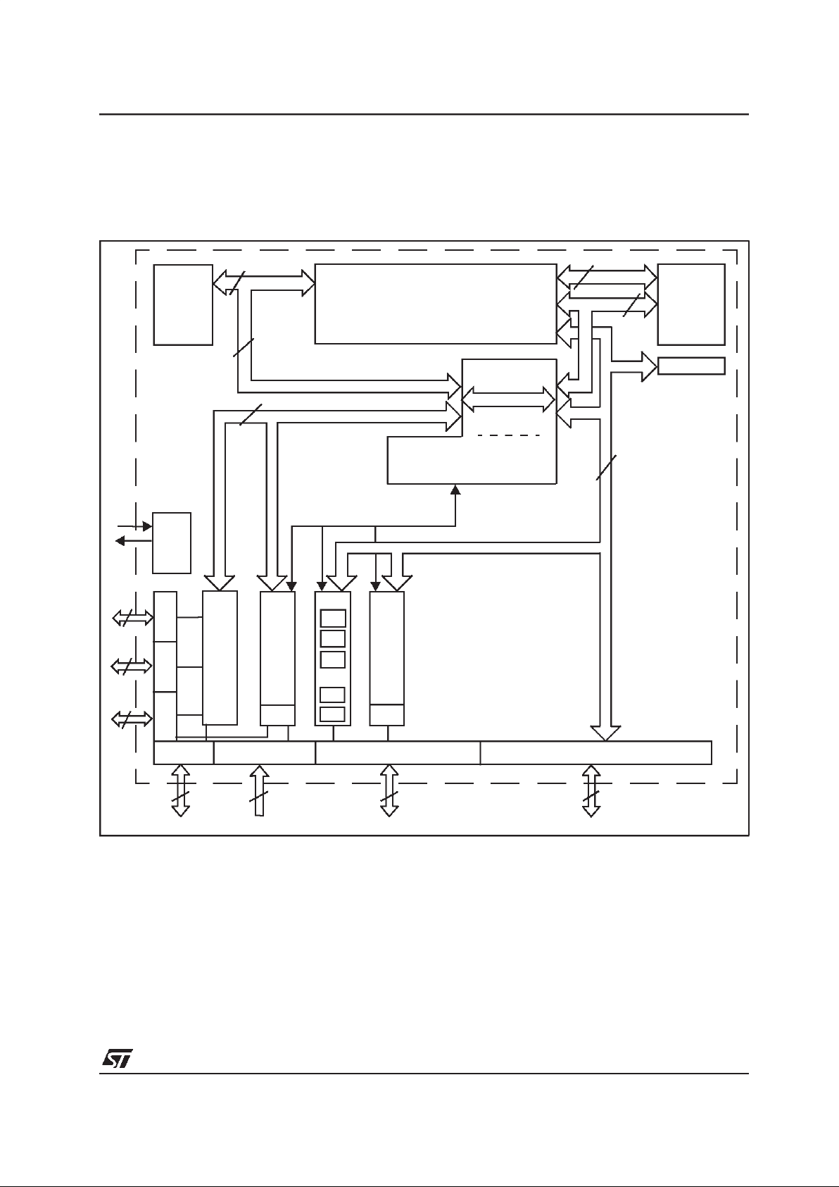
III - FUNCTIONAL DESCRIPTION
The architecture of the ST10F163 combines the
advantages of both RISC and CISC processors
and an advanced peripheral subsystem. The fol-
lowing block diagram gives anoverview of the different on-chip components and of the advanced,
high bandwidth internal busstructure.
Figure 3 : Block diagram
OSC.
Port 0
Port 1Port 4
Port 6
Port 5
Port 3
Port 2
Ext.
Bus
Controller
SSP
BRG
GPT1
T2
T3
T4
GPT2
T5
T6
ASC
(usart)
BRG
Internal
FLASH
Memory
CPU-Core
Internal
RAM
Watchdog
Interrupt Controller
16
16
8
8
8
156
32
16
PEC
16
16
16
16
PLL

ST10F163
10/58
IV - MEMORY ORGANIZATION
The memory spaceof the ST10F163is configured
in a Von-Neumann architecture. Code memory,
data memory, registers and I/O ports are organized within the same linear address space which
includes 16 MBytes. The entire memory space
can be accessed bytewise or wordwise. Particular
portions of the on-chip memory have additionally
been made directly bit addressable.
1 KByte of on-chip RAM is provided as a storage
for user defined variables, for the system stack,
general purposeregister banks and even forcode.
A register bank can consist of up to 16 wordwide
(R0 to R15) and/or bytewide (RL0, RH0, …, RL7,
RH7) General Purpose Registers (GPRs).
1024 bytes (2 * 512 bytes) of the address space
are reserved for the Special Function Register
areas (SFR space and ESFR space). SFRs are
wordwide registers which are used for controlling
and monitoring functions of the different on-chip
units. Unused SFR addresses are reserved for
other/future members of the ST10 family.
In order to meet the needs of system designs
where more memory is required than is provided
on chip, up to 16 MBytes of external RAM and/or
ROM can be connected to themicrocontroller.
V - FLASH MEMORY
The ST10F163 provides 128KBytes of on-chip,
electrically erasable and re-programmable Flash
EPROM. The flash memory is organized in 32 bit
wide blocks. This allows double word instructions
to be fetched in one machine cycle. The flash
memory can be used for both code and data storage. The flash memory is organized into four
banks of sizes 8K, 24K, 48K and 48Kbytes (table
2). Each of these banks can be erased indepen-
dently. This prevents unnecessary erasing of the
whole flash memory whenonly a partial erasing is
required (see Table 2).
Typicaltiming characteristics give 80µs forword or
double word programming and 800 ms for block
erasing, at 25mhz systemclock. the flashmemory
has a typicalendurance of 1000 erasing/programming cycles. the flash memory can be programmed, eitherin a programming board, or inthe
target system. the code to program or erase the
flash memory is executed from an external memory or from theon-chip ram, but not fromthe flash
memory itself. as a flexible and cost-saving alternative, the on-chip bootstrap loader may be used
to load and start the programmingcode.
the following considerations must be taken into
account forprogramming orerasing ‘on-line’in the
target system:
– While operationsare in progress, theflash mem-
ory can not be accessed as usual, no branch
can be made to the flash memory and no data
reads can be taken from the flash memory.
– If the two first blocks (8KB + 24KB) of the flash
memory are mapped to segment 0, no interrupt
or hardware trap must occur during programming or erasing, as this would require a ‘forbidden’ branch to the flashmemory.
A flash memory protection option, whenactivated,
prevents view access to the contents of the ROM
and the on-chip RAM, code operation from within
the flash memory continuesas normal. During the
initialization phase, thefirst two blocks of the flash
memory (8KB + 24KB) can be mapped to segment 0 (addresses 00000h to 07FFFh), or to segment 1 (addresses 10000h to 17FFFh). This
makes itpossible touse external memory for additional system flexibility.
Table 2 : FLASH memory bank organisation
Bank Addresses (Segment 0) Addresses (Segment 1) Size (bytes)
0
1
2
3
000000h to 001FFFh
002000h to 007FFFh
018000h to 023FFFh
024000h to 02FFFFh
010000h to 011FFFh
012000h to 017FFFh
018000h to 023FFFh
024000h to 02FFFFh
8K
24K
48K
48K
ST10F163
11/58
V.1- Programming/erasing with ST Embedded
Algorithm Kernel
In order to secure flash programming and erasing
operations, and also to simplify the software
development for programming and erasing the
Flash, the ST10F163 Flash is programmed or
erased by executing a specific sequence of
instructions (called ‘Unlock Sequence’) with command and parameters loaded into GPRs. The
Unlock Sequence’ invokes embedded kernel routines that checks the validity of the parameters
provided by the user, and decodes the command
(programming or erasing) and executesit.
When performing a programming command, the
Embedded Algorithm Kernel automatically times
the program pulse widths (taking in account the
CPU periodprovided as a parameter by the user)
and verifies proper cell programming.
When performing an erasing command, the
Embedded Algorithm Kernel automatically
pre-programs the bank to be erased if it is not
already programmed. During erase, the Embedded Algorithm Kernel automatically times the
erase pulse widths (taking in account the CPU
period provided as a parameter by the user) and
verifies proper cell erasing.
To start a program/erase operation, the user’s
application must performan ‘Unlock Sequence’ to
trigger the flash ST Embedded Algorithms Kernel
(STEAK). Before using STEAK, proper parameters must be assigned through the R0-R4 registers. TheR0 registeris the command register. The
other registers handle the address and data to be
programmed or sector to be erased. Table 3
defines the command sequence. A definition of
the codes used inTable3 is given in Table 4.
Note The read status for registers R1 to R3 is not used except for the return values, refer to “Return values” on page 13
Table 3 : Command -parameters definition
COMMAND R0 R1 R2 R3 R4
Single word programming 55Ash AddOff W nu 2TCL
Double Word programming DD4sh AddOff DWL DWH 2TCL
Block programming AA5sh BegAddOff EndAddOff SourceAddr 2TCL
Sector Erasing EEEEh 5555h Bnk Bnk 2TCL
Read Status 7777h nu nu nu 2TCL
Table 4 : Code definition
Abbreviation Definition
s Segment of the target flash memory cell
AddOff Segment Offset of thetarget flash memory cell which must be even an value (word-aligned address).
W Data (word) to be written in flash.
DWL,DWH Data (double word, DHL = low word, DWH = high word to be written in Flash,
BegAddOff Segment Offset ofthe FIRST target flash memory word to be written in a multiple programming com-
mand. This value must be even (word-aligned address)
EndAddOff Segment Offset of the LAST Target Flash Memory word to be written in a Multiple programming
command.
Must be even value (word-aligned address). The value D = (EndAddOff - BegAddOff) must be: 0 <=
D < 16384 (ie. up to one page (16 KBytes) can be written in the flash with one multi-word programming command).
SourceAdd Start address for the source data (block) to be programmed. This address uses implicitly the data
paging mechanism of the CPU. SourceAdd value must respect the rules:
- SourceAdd + (EndAddOff - BegAddOff) <16384.
- Page 0 and 1 canNOT be used forsource data if SYSCON bitROMS1 = ‘1’
Note: source data can be located in flash (Inpages 0, 1, 6, 7, 8, 9, 10 or 11 if bit ROMS1 = ‘0’, or in
pages 4, 5, 6, 7, 8, 9,10 or 11if bit ROMS1 = ‘1’.
Bnk Number of the Bank to be erased. Note that for security, R2 and R3 must hold the same value.
2TCL CPU clock period in nseconds (e.g. R4 = 40d means CPU frequency is 25MHz).

ST10F163
12/58
The Flash Unlock Sequence consists of two consecutive writes: the direct addressing mode and
the indirect addressing mode. The FCR must represent an even address in the active address
space of the flash memory. Rwn can be any
unused word GPR (R6 to R15), loaded with a
value that results in the same even address as for
FCR
For easier coding, the standard data paging
addressing schemeis overridden for the two MOV
instruction of the Flash Trigger Sequence (EXTS
instruction). This also locked both standard and
PEC interrupts and class A hardware traps. Must
be replace by ATOMICinstruction if standardDPP
addressing scheme must be preserved.
When the embedded programming/erasing algorithm returns to trigger point, information can be
collected through registerR0 so the user can take
specific actions. Table 5 lists all of the error codes
that can be returned in R0.
Note The Flash Embedded Presto Algorithms require at least 45 words on the Internal System Stack for proper operation. The program
verifies itself that there is enough free space on the System Stack before performing a programming or erasing operation (by
comparing SP value with STKOV+90d).
EXTS #1, #2 ; assumes flash is
mapped in seg 1
MOV FCR, R7 ; first part
MOV [R7], R7 ; second part
Table 5 : Error code definition
ERROR CODE MEANING
00h Operation was successful
01h ROMEN bit inside SYSCON is not set
02h Vpp voltage not present
03h Programming operation failed
04h Address value (R1) incorrect: not in Flash address area or odd
05h CPU period out of range (must be between 10 ns to 1000 ns)
06h Not enough free space on system stack for proper operation
07h Incorrect bank number (R2,R3) specified
08h Erase operation failed
09h Bad source address for multi-word programming command
0Ah Bad number of words to be copied in multi-word programming command: one
destination will be outof flash, or one source operand will be out of the source page
FFh Unknown or bad command

ST10F163
13/58
V.1.1- Return values
After a single or double word programming command, R0 contains error code, R1 remains
unchanged, R2 will contain the data in Flash for
location Segment+Segment Offset (R0.[3:0] with
R1), R3 will contain the data in Flash for location
Segment+Segment Offset +2 (R0[3:0] withR1+2),
R4 to R15 remain unchanged.
After a multi-word programming command, R0
contains error code, R1 will contains the last segment offset address of the last written word in
flash (failing flash address if R0 is not equal to
zero), R2 and R3 are undefined, R4 to R15
remain unchanged.
After erasing command, only R4 to R15 remain
unchanged, R0 will contain error code, R1 to R3
are undefined.
After status read command, R0 contains error
code, R1 contains flash embedded revision, R2
and R3 contains circuit identifiers (R2 = #0787h
and R3 = #0101h for this device), R4 to R15
remain unchanged.
V.1.2- Programming examples
Programming a double word:
Note For easier coding, the standard data paging addressing scheme is overrides for the two MOV instruction of the Flash Trigger
Sequence (EXTS instruction).This also locked both standard and PEC interrupts and class A hardware traps. Must be replace by
ATOMIC instruction if standard DPP addressing scheme must be preserved.
Programming a block of data:
Address 01’9000h to 01’9FFEh (inclusive) is to be programmed. Source data (data to be copied into
flash) is located in external RAM from address 03’1000h (to 03’1FFEh, implicitly):
; code hereafter assumes that flash is mapped in segment 1
; i.e. bit ROMS1 = ‘1’ in SYSCON register
; Flash must also be enabled, i.e. bit ROMEN = ‘1’ in SYSCON.
MOV R0, #PROGDW ; DD4xh: Double word programming command
OR R0, #01h ; Selects segment 1 in flash memory
MOV R1, #00224h ; Address to be programmed is 01’0224h
MOV R2, #03456h ; Data to be programmed at 01’0224h
MOV R3, #04567h ; Data to be programmed at 01’0226h
MOV R4, #050d ; 50ns is 20 MHz CPU clock frequency
MOV R7, #08000h ; R7 used for Flash trigger sequence
#define FCR 08000h
; Flash Unlock Sequence: consists in two consecutive writes, with the direct
addressing mode and then the indirect addressing mode. FCR must represent an
even address in the active address space of the Flash memory, and Rwn can be
any unused word GPR (R6 to R15)loaded with a value resulting in the same even
address than FCR
EXTS #1, #2 ; flash can be mapped in segment 0 or 1
MOV FCR, R7 ; first part
MOV [R7], R7 ; second part
NOP ; WARNING: place 2 NOP operations after
NOP ; the Unlock sequence to avoid all possible
; pipeline conflict in STEAK programs
; code hereafter assumes that flash is mapped in segment 1
; i.e. bit ROMS1 = ‘1’ in SYSCON register
; Flash must also be enabled, i.e. bit ROMEN = ‘1’ in SYSCON.
MOV R0, #PROGMW ; AA5xh: Multi word programming command
OR R0, #01h ; Selects segment 1 in flash memory

ST10F163
14/58
V.2- Flash memory configuration
The default memory configuration is determined
by the state of the EA pin at reset. This value is
stored in the Internal ROM enable bit: ROMEN of
the SYSCON Register.
When ROMEN=0, the internal ROM is disabled
and externalROM is used for start-up control.The
first 32KBytes of the flash memory area must be
re-mapped to segment 1, to enabletheir later use.
This is done by setting the ROMS1 bit of
SYSCON to 0. This is done by the externally supplied program, before the execution of the EINIT
instruction.
If program execution startsfrom external memory,
but access to the flash memory (re-mapped to
Bank 1) is required later, one of the following values has to be written to the SYSCON register,
before the end of initialization:
– If flash is to be mapped to segment 1:
xxx100xxxxxxxxxxb
(ROMS1=1,SGTDIS=0)
– If flash is to be mapped to segment 0:
xxx000xxxxxxxxxxb
(ROMS1=0,SGTDIS=0)
All other parts of the flash memory (addresses
18000h - 1FFFFh) remain unaffected.
The SGTDIS Segmentation Disable/Enable must
be set to 0 so that the 64KBytes of on-chip memory can be used in addition to the external boot
memory. The correct procedure for changing the
segmentation registers must be observed, to prevent unwanted trap conditions:
– Instructions that configure the internal memory
must only be executed from external memory
or from the internal RAM.
– Whenever the internalmemory is disabled,ena-
bled or re-mapped, the DPPs must be explicitly
(re)loaded to enable correct data accesses to
the internal memory and/or externalmemory.
V.3 - Flash protection
The flash protection mode, prevents the reading
of data operands in the flashmemory by anything
but a program executed from the flash memory
itself. Flash protection mode permits program
branches from, or into the flash memory, but does
not permit erasing and programming of the flash
memory.
Flash protection is controlled by the Protection
UPROM Programming Bit(UPROG). UPROG is a
’hidden’ one-time programmable bit. It is only
accessible in a special mode, entered, for example, via a flash EPROM programming board. If
UPROG is setto ‘1’,flash protection isactive after
reset. By default flash protection is disabled
(UPROG=0).
For deactivation of flash protection, where the
flash memory has to be reprogrammed with
updated program/variables, a zero value must be
written at every even address in the active
address spaceof the flash memory.This write can
only be done by an instruction executed from the
internal flash memory itself, e.g. MOV
FLASH,ZEROS.
MOV R1, #09000h ; First Flash Segment Offset Address
MOV R2, #09FFEh ; Last Flash Segment Offset Address
MOV R3, #01000h ; Source data address: use DPP2 as
; data page pointer
SCXT DPP2,#0Ch ; Source is in page 12 (0Ch): save previous
; DPP2 value and load it with source page
; number
MOV R4, #050d ; 50ns is 20 MHz CPU clock frequency
MOV R7, #08000h ; R7 used for Flash trigger sequence
#define FCR 08000h
EXTS #1, #2 ; flash can be mapped in segment 0 or 1
MOV FCR, R7 ; first part
MOV [R7], R7 ; second part
NOP ; WARNING: place 2 NOP operations after
NOP ; the Unlock sequence to avoid all possible
; pipeline conflict in STEAK programs
POP DPP2 ; restore DPP2

ST10F163
15/58
VI - EXTERNAL BUS CONTROLLER
All of the external memory accesses are performed by a particular on-chip External Bus Controller (EBC). It can be programmed either to
Single Chip Mode when no external memory is
required, or to one of four different external memory access modes:
– 16-/18-/20-/24-bit Addresses, 16-bit Data, De-
multiplexed
– 16-/18-/20-/24-bit Addresses, 16-bit Data, Multi-
plexed
– 16-/18-/20-/24-bit Addresses, 8-bit Data, Multi-
plexed
– 16-/18-/20-/24-bit Addresses, 8-bit Data, De-
multiplexed
In the demultiplexed bus modes, addresses are
output on PORT1 and data is input/output on
PORT0 or P0L, respectively. In the multiplexed
bus modes both addresses and data use PORT0
for input/output.
Important timing characteristics of the external
bus interface (Memory Cycle Time, Memory
Tri-State Time, Length of ALE and Read Write
Delay) have been made programmable. This
gives the choice of a wide range of different types
of memories and external peripherals. In addition,
up to 4 independent address windows may be
defined (via register pairs ADDRSELx / BUSCONx).
This gives access to different resources with different bus characteristics. These address windows are arranged hierarchically where
BUSCON4 overrides BUSCON3 and BUSCON2
overrides BUSCON1.
All accesses to locations not covered by these 4
address windows are controlled by BUSCON0.
Up to 5 external CS signals (4 windows plus
default) canbe generated in order tosave external
glue logic. Access to very slow memories is supported via a particular ‘Ready’ function.
A HOLD/HLDA protocol is available for bus arbitration so that external resources can be shared
with other bus masters. The bus arbitration is
enabled by setting bit HLDEN in register
SYSCON. After setting HLDEN once, pins
P6.7...P6.5 (BREQ, HLDA, HOLD) are automatically controlled by the EBC. In Master Mode
(default after reset) the HLDA pin is an output.
By setting bit DP6.7 to’1’ the Slave Mode is
selected where pin HLDA is switched to input.
This allows to directly connect the slave controller
to another master controller withoutglue logic.
For applications which require less than 16
MBytes of external memory space, this address
space can be restricted to 1 MByte, 256 KByte or
to 64 KByte. In this case Port 4 outputs four, two
or no address lines at all. If an address space of
16 MBytes is used,it outputs all 8 address lines.
Note When the on-chip SSP Module is to be used the segment
address output on Port 4 must be limited to 4 bits (i.e.
A19...A16) in order to enable the alternate function of the
SSP interface pins.
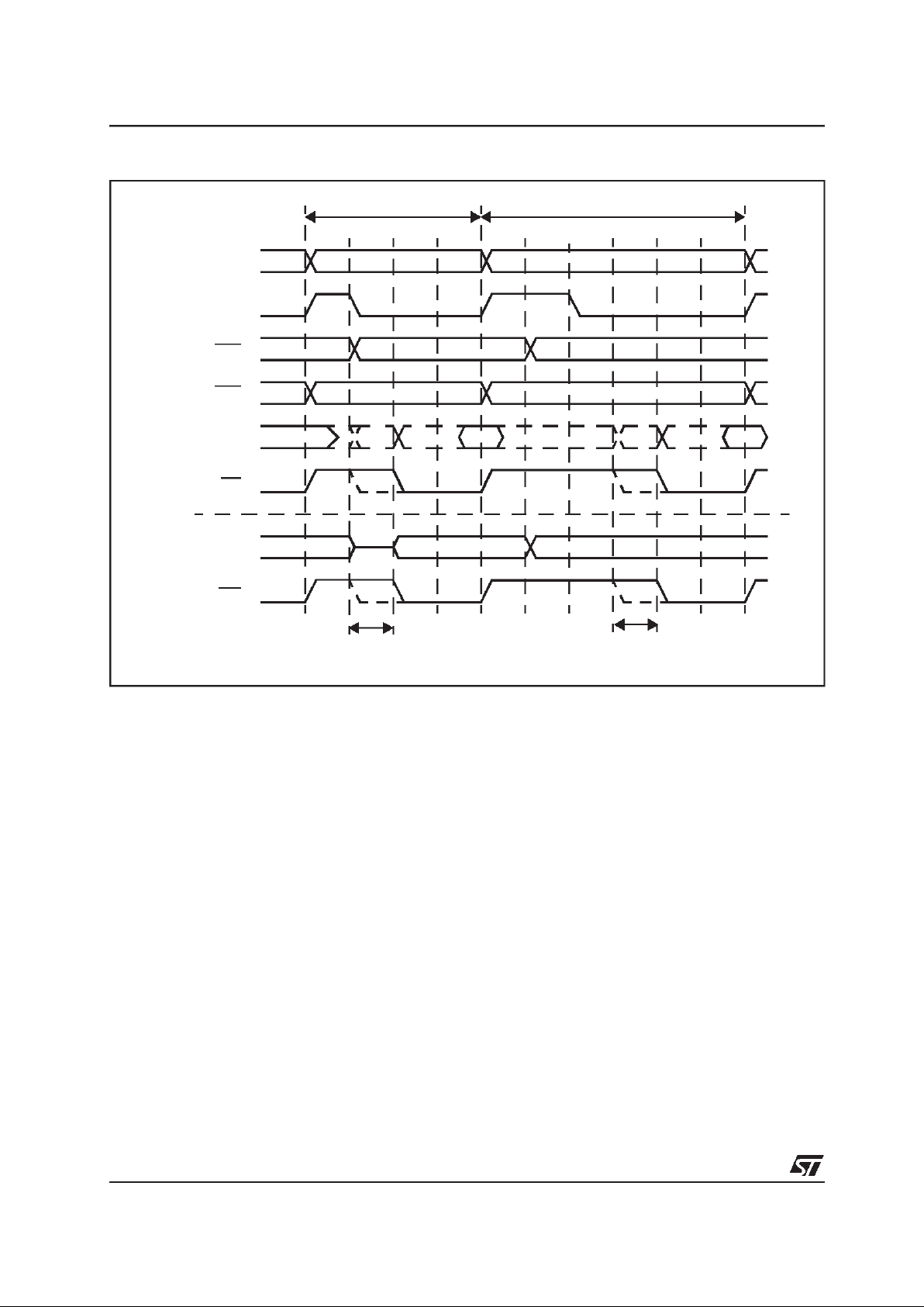
VI.1 - Programmable chip select timing control
The position of the CSx lines can be changed by
setting theCSCFG bit inthe SYSCON register. By
default the CSx lines change half a CPU clock
cycle after the rising edge of ALE (20ns @ f
CPU
=
25 MHz). With the CSCFG bit set (section
Figure VII -
), the CSx lines change with the rising
edge of ALE. In this case, the CSx lines and
address lines change at the same time.
ST10F163
16/58
Figure 4 : Chip selectdelay
Delay
Normal CSx
RD
Address (P1)
ALE
Segment (P4)
NormalDemulti plexed
Bus Cycle
ALE Lengthen Demultiplexed
BusCycle
Unlatched CSx
WR
Data Data
Data
BUS(P0)
BUS(P0)
Read/Write
Delay
Read/Write
Data

ST10F163
17/58
VII - CENTRAL PROCESSING UNIT (CPU)
The main core of the CPU consists of a 4-stage
instruction pipeline, a 16-bit arithmetic and logic
unit (ALU) and dedicated SFRs. Additional hardware has been added for a separate multiply and
divide unit, a bit-mask generator and a barrel
shifter.
Based on these hardware provisions, most of the
ST10F163’s instructions can be executed in one
machine cycle. This requires 80ns at 25MHz CPU
clock. For example, shift and rotate instructions
are always processed in one machine cycle independent of the number of bits to be shifted. All
multiple-cycle instructions have been optimized
for speed: branches in 2 cycles,a 16 x 16 bit multiplication in 5 cycles and a 32-/16 bit division in
10 cycles. The ‘Jump Cache’ pipeline optimization, reduces the execution time of repeatedly performed jumps in aloop, from 2 cycles to 1 cycle.
The CPU includes an actual register context.This
consists of up to 16 wordwide GPRs physically
allocated in the on-chip RAM area. A Context
Pointer (CP) register determines the base
address ofthe activeregister bank to be accessed
by the CPU. The number of register banks is only
restricted by the available internal RAM space.
For easy parameter passing, one register bank
may overlap others.
A system stack ofup to 1024 bytes is provided as
a storage for temporary data. The system stack is
allocated in the on-chip RAM area, and it is
accessed by the CPU via the stack pointer (SP)
register. Two separate SFRs, STKOV and
STKUN, are implicitly compared against the stack
pointer value upon each stack access for the
detection of a stack overflow or underflow.
The basic instruction length is either 2 or 4 bytes.
Possible operand typesare bits, bytes andwords.
A variety of direct, indirect or immediate addressing modes exist.
Figure 5 : CPU block diagram
16
16
32
ROM
Internal
RAM
1KByte
R15
R0
General
Purpose
Registers
R0
R15
MDH
MLD
Barrel-Shift
Mul./Div.-HW
Bit-Mask Gen.
ALU
16-Bit
Context Ptr
SP
STKOV
STKUN
Exec. Unit
Instr. Ptr
Instr. Reg
4-Stage
Pipeline
PSW
SYSCON
BUSCON 0
BUSCON 1
BUSCON 2
BUSCON 3
BUSCON 4
ADDRSEL 1
ADDRSEL 2
ADDRSEL 3
ADDRSEL 4
Data Pg. Ptrs Code Seg. Ptr.
CPU
128KBytes
FLASH

ST10F163
18/58
VIII - INTERRUPT SYSTEM
With an interrupt response time from 200 ns to
480ns (in the case of internal program execution),
the ST10F163 reacts quickly to the occurrence of
non-deterministic events.
The architecture of the ST10F163 supports several mechanisms for fast and flexible response to
service requests that can be generated from various sources internal or external to the microcontroller. Any of these interrupt requests can be
programmed to being serviced by the Interrupt
Controller or by the Peripheral Event Controller
(PEC). In a standard interrupt service, program
execution is suspended and a branch to the interrupt vector table is performed. For a PEC service,
just one cycle is ‘stolen’ from the current CPU
activity. A PEC service is a single byte or word
data transfer between any two memory locations
with an additional increment of either the PEC
source or the destination pointer. An individual
PEC transfer counter is decremented for each
PEC service, except for the continuous transfer
mode. When this counter reaches zero, a standard interrupt is performed to the corresponding
source related vector location. PEC services are
suited to, for example, the transmission or reception of blocks of data. The ST10F163 has 8 PEC
channels, each of which offers fast interrupt-driven data transfer capabilities.
A separate control register which contains an
interrupt request flag, an interrupt enable flag and
an interrupt priority bitfield, exists for each of the
possible interrupt sources. Via its related register,
each source can be programmed to one ofsixteen
interrupt priority levels. Once having been
accepted by the CPU, an interrupt service can
only be interrupted by a higher prioritized service
request. For the standard interrupt processing,
each of the possible interrupt sources has a dedicated vector location.
Fast external interrupt inputs are provided to service external interrupts with high precision
requirements. These fast interrupt inputs, feature
programmable edge detection (rising edge, falling
edge or both edges).
Software interruptsare supportedby means of the
‘TRAP’ instruction in combination with an individual trap (interrupt) number.
Table 6 shows all of the possible ST10F163 interrupt sources and the corresponding hardware-related interrupt flags, vectors, vector
locations and trap (interrupt) numbers:
Table 6 : List of possible interrupt sources, flags,vector and trap numbers
Source of Interrupt or PEC
Service Request
Request
Flag
Enable
Flag
Interrupt
Vector
Vector
Location
Trap
Number
External Interrupt 0 CC8IR CC8IE CC8INT 00’0060h 18h
External Interrupt 1 CC9IR CC9IE CC9INT 00’0064h 19h
External Interrupt 2 CC10IR CC10IE CC10INT 00’0068h 1Ah
External Interrupt 3 CC11IR CC11IE CC11INT 00’006Ch 1Bh
External Interrupt 4 CC12IR CC12IE CC12INT 00’0070h 1Ch
External Interrupt 5 CC13IR CC13IE CC13INT 00’0074h 1Dh
External Interrupt 6 CC14IR CC14IE CC14INT 00’0078h 1Eh
External Interrupt 7 CC15IR CC15IE CC15INT 00’007Ch 1Fh
GPT1 Timer 2 T2IR T2IE T2INT 00’0088h 22h
GPT1 Timer 3 T3IR T3IE T3INT 00’008Ch 23h
GPT1 Timer 4 T4IR T4IE T4INT 00’0090h 24h
GPT2 Timer 5 T5IR T5IE T5INT 00’0094h 25h
GPT2 Timer 6 T6IR T6IE T6INT 00’0098h 26h
GPT2 CAPREL Register CRIR CRIE CRINT 00’009Ch 27h
ASC0 Transmit S0TIR S0TIE S0TINT 00’00A8h 2Ah
ASC0 Transmit Buffer S0TBIR S0TBIE S0TBINT 00’011Ch 47h
ASC0 Receive S0RIR S0RIE S0RINT 00’00ACh 2Bh
ASC0 Error S0EIR S0EIE S0EINT 00’00B0h 2Ch

ST10F163
19/58
The ST10F163 provides an excellent mechanism
to identify and to process exceptions orerror conditions that arise during run-time, called‘Hardware
Traps’.
Hardware traps cause an immediate
non-maskable system reaction which is similar to
a standard interrupt service (branching to a dedicated vector table location). The occurrence of a
hardware trap is additionally signified by an indi-
vidual bit in the trap flag register (TFR). Except
when another higher prioritized trap service is in
progress, a hardware trap will interrupt any actual
program execution. In turn, hardware trap services can normally not be interrupted by standard
or PEC interrupts.
Table 7 shows all of the possible exceptions or
error conditions that can arise during run time.
SSP Interrupt XP1IR XP1IE XP1INT 00’0104h 41h
PLL Unlock / OWD XP3IR XP3IE XP3INT 00’010Ch 43h
Table 6 : List of possible interrupt sources, flags,vector and trap numbers (continued)
Source of Interrupt or PEC
Service Request
Request
Flag
Enable
Flag
Interrupt
Vector
Vector
Location
Trap
Number
Table 7 : Exceptions or error conditions that can arise during run-time
Exception Condition
Trap
Flag
Trap
Vector
Vector
Location
Trap
Number
Trap
Priority
Reset Functions:
Hardware Reset RESET 00’0000h 00h III
Software Reset RESET 00’0000h 00h III
Watchdog Timer Overflow RESET 00’0000h 00h III
Class A Hardware Traps:
Non-Maskable Interrupt NMI NMITRAP 00’0008h 02h II
Stack Overflow STKOF STOTRAP 00’0010h 04h II
Stack Underflow STKUF STUTRAP 00’0018h 06h II
Class B Hardware Traps:
Undefined Opcode
UNDOPC BTRAP 00’0028h 0Ah I
Protected Instruction Fault
PRTFLT BTRAP 00’0028h 0Ah I
Illegal Word Operand Access
ILLOPA BTRAP 00’0028h 0Ah I
Illegal Instruction Access
ILLINA BTRAP 00’0028h 0Ah I
Illegal External Bus Access
ILLBUS BTRAP 00’0028h 0Ah I
Reserved [2Ch –3Ch] [0Bh – 0Fh]
Software Traps:
TRAP Instruction
Any
[00’0000h–
00’01FCh]
in steps of4h
Any
[00h – 7Fh]
Current
CPU
Priority

ST10F163
20/58
IX - GENERAL PURPOSE TIMER(GPT) UNIT
The GPT unit is a flexible multifunctional timer/
counter structure which is used for time related
tasks such as event timing and counting, pulse
width and duty cycle measurements,pulse generation, or pulse multiplication. The GPT unit contains five 16-bit timersorganized intotwo separate
modules GPT1 and GPT2. Each timer in each
module may operate independently in several different modes, or may be concatenated with
another timer of the same module.
IX.1 - GPT1
Each of the three timers T2, T3, T4 of module
GPT1 can be configured individually for one of
three basic modes of operation: timer, gated
timer, and counter mode. In Timer Mode, the
input clock for a timer is derived from the CPU
clock, divided by a programmable pre-scaler. In
counter Mode a timer is clocked in reference to
external events. Gated timer modesupports pulse
width or duty cycle measurement,where the operation of a timer is controlled by the ‘gate’ level on
an external input pin. Each timer has one associated port pin (TxIN) which servesas gate or clock
input.
Table 8 lists the timer input frequencies, resolution
and periods for each pre-scaler option at 25 MHz
CPU clock (see Table 8).
The count direction (up/down) for each timer is
programmable by software or is altered dynamically by an external signal on a port pin (TxEUD).
For example, this facilitates position tracking.
Timer T3has output toggle latches (TxOTL)which
changes state on each timer over-flow/underflow.
The state of this latch may be output on port pins
(TxOUT) e. g. for time out monitoring of external
hardware components, or may be used internally
to clock timers T2 and T4 for measuring long time
periods with high resolution.
In addition to their basic operating modes, timers
T2 and T4 may be configured as reloador capture
registers for timer T3. When used as reload or
capture registers, timers T2 and T4 are stopped.
The content of timer T3 is captured into T2 or T4
in response to a signal at their associated input
pins (TxIN). Timer T3 is reloaded with the contents of T2 or T4, triggered, either by an external
signal or by a selectable state transition of its toggle latch, T3OTL. When both T2 and T4 are configured to alternately reload T3 on opposite state
transitions of T3OTL with the low and high times
of a PWM signal, this signal can be constantly
generated without software intervention.
IX.2 - GPT2
The GPT2 module provides precise event control
and time measurement. It includestwo timers (T5,
T6) anda capture/reload register (CAPREL). Both
timers can be clocked with an input clock which is
derived from the CPU clock via a programmable
prescaler or with external signals. The count
direction (up/down) for each timer is programmable by software or may additionally be altered
dynamically by an external signal on a port pin
(TxEUD). Concatenation of the timers is supported via the output togglelatch (T6OTL) of timer
T6 which changes its state on each timer overflow/underflow.
The state of this latch may be used to clock timer
T5, or it may beoutput on aport pin (T6OUT).The
overflows/underflows of timer T6 can additionally
be used to clock the CAPCOM timers T0 or T1,
and to cause a reload from the CAPREL register.
The CAPREL registermay capture the contents of
timer T5 based on an external signal transition on
the corresponding port pin (CAPIN), and timer T5
may optionally be cleared after the capture procedure. This allows absolute time differences to be
measured or pulse multiplication to be performed
without software overhead.
Table 9 lists the timer input frequencies, resolution
and periods for each pre-scaler option at 25 MHz
CPU clock.
Table 8 : GPT1timer input frequencies, resolution and periods
f
CPU
= 25MHz
Timer InputSelection T2I / T3I / T4I
000
B
001
B
010
B
011
B
100
B
101
B
110
B
111
B
Pre-scaler factor 8 16 32 64 128 256 512 1024
Input Frequency 3.125MHz 1.563MHz 781.3kHz 390.6kHz 195.3kHz 97.66kHz 48.83kHz 24.41kHz
Resolution 320 ns 640 ns 128 ns 2.56 µs 5.12 µs 10.24 µs 20.48 µs 40.96 µs
Period 21.0 ms 41.9 ms 83.9 ms 167 ms 336 ms 671 ms 1.34 s 2.68 s
ST10F163
21/58
Table 9 : GPT2 timer input frequencies, resolution andperiod
f
CPU
= 25MHz
Timer Input Selection T5I / T6I
000
B
001
B
010
B
011
B
100
B
101
B
110
B
111
B
Pre-scaler factor 4 8 16 32 64 128 256 512
Input Frequency 6.25MHz 3.125MHz 1.563MHz 781.3kHz 390.6kHz 195.3kHz 97.66kHz 48.83kHz
Resolution 160ns 320 ns 640 ns 128 ns 2.56 µs 5.12 µs 10.24 µs 20.48 µs
Period 10.49ms 21.0 ms 41.9 ms 83.9 ms 167 ms 336 ms 671 ms 1.34 s
Figure 6 : Block diagram of GPT1
2nn=3...10
2
n
n=3...10
2
n
n=3...10
T2EUD
T2IN
CPU Clock
CPU Clock
CPU Clock
T3IN
T4IN
T3EUD
T4EUD
T2
Mode
Control
T3
Mode
Control
T4
Mode
Control
GPT1 TimerT2
GPT1 Timer T3
GPT1 TimerT4
T3OTL
Reload
Capture
U/D
U/D
Reload
Capture
Interrupt
Request
Interrupt
Request
Interrupt
Request
T3OUT
U/D

ST10F163
22/58
Figure 7 : Block diagram of GPT2
2nn=2...9
2
n
n=2...9
T5EUD
T5IN
CPUClock
CPUClock
T6IN
T6EUD
T5
Mode
Control
T6
Mode
Control
GPT2 Timer T5
GPT2Timer T6
U/D
Interrupt
Request
U/D
GPT2 CAPREL
T60TL
Toggle FF
T6OUT
CAPIN
Reload
Interrupt
Request
Capture
Clear
Interrupt
Request

ST10F163
23/58
X - PARALLEL PORTS
The ST10F163 provides up to 77 I/O lines which
are organized into six input/output ports and one
input port. All portlines are bit-addressable, and all
input/output lines are individually (bit-wise) programmable as, either inputsor outputsvia direction
registers. The I/O ports are true bidirectional ports
which are switched to high impedance state when
configured as inputs. The output drivers of three I/
O ports can be configured (pin by pin) for push/pull
operation or open-drainoperation via control registers. During the internalreset, all port pinsare configured as inputs. All port lines have associated,
programmable, alternate input or output functions.
PORT0 and PORT1 may be used as address and
data lines when accessing externalmemory. Port4
outputs the additional segment address bits A23/
19/17...A16 in systems where segmentation is
enabled to access more than 64 KBytes of memory.Port 6 provides optional bus arbitration signals
(BREQ, HLDA, HOLD) and chipselectsignals. Port
3 includes alternatefunctions of timers,serial interfaces, the optional bus control signal BHE and the
system clock output (CLKOUT). Port 5 is used for
timer control signals.All portlines thatare not used
for these alternate functions may be used as general purpose I/O lines.
XI - SERIAL CHANNELS
Serial communication with other microcontrollers,
processors, terminals or external peripheral com-
ponents is provided by two serial interfaces, an
Asynchronous/Synchronous Serial Channel
(ASC0) and a Synchronous Serial Port (SSP).
ASC0: The table below shows the baud rates for
the asynchronous/synchronous serial channel.
A dedicated baud rate generator is used to set up
all standard baud rateswithout oscillator tuning. 3
separate interrupt vectors are provided for transmission, reception, and erroneous reception. In
asynchronous mode, 8- or 9-bit data frames are
transmitted or received, preceded by a start bit
and terminated by one or two stop bits. For multiprocessor communication, a mechanism to distinguish address from data bytes has been included
(8-bit data + wake up bit mode). In synchronous
mode, the ASC0 transmits or receives bytes (8
bits) synchronously toa shiftclock which is generated by the ASC0. The ASC0 always shifts the
LSB first.Aloop backoption isavailable fortesting
purposes. A number of optional hardware error
detection capabilities have been included to
increase the reliability of data transfers. A parity
bit can automatically be generated on transmission or be checked on reception. Framing error
detection allows to recognize data frames with
missing stop bits. An overrun error will be generated, if the last character received has not been
read out of the receive buffer register by the time
the reception of a new characteris complete.
Note Thedeviationerrorsgiven inthe tableabovearerounded.Usinga baudratecrystalwillprovidecorrectbaudrateswithoutdeviationerrors.
Table 10 : Commonly used baud rates by reload value and deviation errors
S0BRS = ‘0’, f
CPU
= 25MHz S0BRS = ‘1’, f
CPU
= 25MHz
Baud Rate
(Baud)
Deviation Error Reload Value
Baud Rate
(Baud)
Deviation Error Reload Value
781250 ±0.0% 0000
H
520833 ±0.0% 0000
H
56000 +7.3% /-0.4% 000CH/ 000D
H
56000 +3.3% / -7.0% 0008H / 0009H
38400 +1.7% / -3.1% 0013
H
/ 0014
H
38400 +4.3% / -3.1% 000CH / 000DH
19200 +1.7% / -0.8% 0027
H
/ 0028
H
19200 +0.5% / -3.1% 001AH / 001BH
9600 +0.5% / -0.8% 0050
H
/ 0051
H
9600 +0.5% / -1.4% 0035H / 0036H
4800 +0.5% / -0.1% 00A1
H
/ 00A2
H
4800 +0.5% / -0.5% 006BH / 006CH
2400 +0.2% / -0.1% 0144
H
/ 0145
H
2400 +0.0% / -0.5% 00D8H / 00D9H
1200 +0.0% / -0.1% 028A
H
/ 028B
H
1200 +0.0% / -0.2% 01B1H / 01B2H
600 +0.0% / -0.1% 0515
H
/ 0516
H
600 +0.0% / -0.1% 0363H / 0364H
95 +0.4% / 0.4% 1FFF
H
/ 1FFF
H
75 +0.0% / 0.0% 1B1FH / 1B20H
63 +0.9% / 0.9% 1FFFH / 1FFFH

ST10F163
24/58
SSP: The Synchronous Serial Port provides
high-speed serial communication with external
slave devices such as EEPROM. The SSP transmits 1...3 bytes or receives 1 byte after sending
1...3 bytes synchronously to a shift clock which is
generated by the SSP.
The SSP canstart shifting withthe LSB or with the
MSB and is used to select shifting and latching
clock edgesas wellas theclock polarity. Up totwo
chip selectlines may be activatedin order todirect
data transfers to one or both of two peripheral
devices.
Table 11 : Synchronousbaud rate and SSPCKS reload values
SSPCKS Value Synchronous baud rate
000 SSP clock = CPU clock divided by 2 12.5 MBit/s
001 SSP clock = CPU clock divided by 4 6.25 MBit/s
010 SSP clock = CPU clock divided by 8 3.13 MBit/s
011 SSP clock = CPU clock divided by 16 1.56 MBit/s
100 SSP clock = CPU clock divided by 32 781 KBit/s
101 SSP clock = CPU clock divided by 64 391 KBit/s
110 SSP clock = CPU clock divided by 128 195KBit/s
111 SSP clock = CPU clock divided by 256 97.7 KBit/s

ST10F163
25/58
XII - WATCHDOG TIMER
The Watchdog Timer is a fail-safe mechanism
which the maximum malfunction time of the controller
The Watchdog Timer is always enabled after a
reset of the chip, and can only be disabled in the
time interval until the EINIT (end of initialization)
instruction has been executed. In this way the
chip’s start-up procedure is always monitored.
The software must be designed to service the
Watchdog Timer before it overflows. If, due to
hardware or software related failures, thesoftware
fails to do so, the Watchdog Timer overflows and
generates an internal hardware reset and pulls
the RSTOUT pin low in order to allow external
hardware components to be reset.
The Watchdog Timer is a 16-bit timer, clocked
with the system clock divided either by 2 or by
128. The high byte of the WatchdogTimer register
can be set to a pre-specified reload value (stored
in WDTREL) in order to allow further variation of
the monitored time interval. Each time it is serviced by the application software, the high byte of
the Watchdog Timer is reloaded. The Table12
shows the watchdog time range which for a
25MHz CPU clock. Some numbersare roundedto
3 significant digits.
XIII - OSCILLATOR WATCHDOG (OWD)
The Oscillator Watchdog (OWD) monitors the
clock signal generated by the on-chip oscillator
(either with a crystal or via external clock drive).
For this operation the PLL provides a clock signal
to supervise transitions on the oscillator clock.
This PLL clock is independent from the XTAL1
clock. When the expected oscillator clock transitions are missing, the OWD activates the PLL
Unlock/OWD interrupt node and supplies the CPU
with the PLL clock signal. Under these circumstances the PLL will oscillate with its basic frequency.
A low level onpin OWE disables the OWD’sinterrupt output, sothat theclock signalis derived from
the oscillator clock. The CPU clock source is only
switched back to the oscillator clock after a hardware reset.
When the direct-drive, or direct-drive-with- prescaler clock option is selected, an oscillator watchdog is implemented. This provides a fail-safe
mechanism in the case of a lossof external clock.
After reset, the Oscillator Watchdogis enabled by
default. To disable the OWD, the bit OWDDIS (bit
4 of SYSCON register) must be set. When the
OWD is enabled, PLL runs on free-running frequency, and increments the Oscillator Watchdog
counter. On each transition of XTAL1 pin, the
Oscillator Watchdog is cleared. If an external
clock failure occurs, then the Oscillator Watchdog
counter overflows (after16 PLL clockcycles). The
CPU clock signal is switched to the PLL free-running clock signal, and the Oscillator Watchdog
Interrupt Request (XP3INT) is flagged. The CPU
clock will not switch back to the external clock
even if a valid external clock exits on XTAL1 pin.
Only a hardware reset can switch the CPU clock
source back to direct clock input.
When the OWD is disabled, the CPU clock is
always fed from theoscillator input and the PLL is
switched off to decrease power supply current.
Note For security,rewrite WDTCON each time before the watchdog timer is serviced.
Table 12 : Watchdogtime range for 25MHz CPU clock
Reload value
in WDTREL
Prescaler for f
CPU
2 (WDTIN = ‘0’) 128 (WDTIN = ‘1’)
FF
H
20.48 µs 1.31 ms
00
H
5.24 ms 336 ms

ST10F163
26/58
XIV - INSTRUCTION SET SUMMARY
The table below lists the instruction set of the
ST10F163.
More detailed information such as address
modes, instruction operation, parameters for con-
ditional execution of instructions, opcodes and a
detailed description of each instruction can be
found in the “ST10 Family Programming Man-
ual”
Table 13 : Instruction Set
Mnemonic Description Bytes
ADD(B) Add word (byte) operands 2 / 4
ADDC(B) Add word (byte) operands with Carry 2 / 4
SUB(B) Subtract word (byte) operands 2 / 4
SUBC(B) Subtract word (byte) operands with Carry 2 / 4
MUL(U) (Un)Signed multiply direct GPR by direct GPR (16-16-bit) 2
DIV(U) (Un)Signed divide register MDL by direct GPR (16-/16-bit) 2
DIVL(U) (Un)Signed long divide reg. MDby direct GPR (32-/16-bit) 2
CPL(B) Complement direct word (byte) GPR 2
NEG(B) Negate direct word (byte) GPR 2
AND(B) Bitwise AND, (word/byte operands) 2 / 4
OR(B) Bitwise OR, (word/byte operands) 2 / 4
XOR(B) Bitwise XOR, (word/byte operands) 2 /4
BCLR Clear direct bit 2
BSET Set direct bit 2
BMOV(N) Move (negated) direct bit to direct bit 4
BAND, BOR, BXOR AND/OR/XOR direct bit with direct bit 4
BCMP Compare direct bit todirect bit 4
BFLDH/L Bitwise modify masked high/low byte of bit-addressable direct word memory
with immediate data
4
CMP(B) Compare word (byte) operands 2 / 4
CMPD1/2 Compare word data to GPR and decrement GPR by 1/2 2 / 4
CMPI1/2 Compare word data to GPR and increment GPR by 1/2 2 / 4
PRIOR Determine number of shift cycles to normalize direct word GPR and store
result in direct word GPR
2
SHL / SHR Shift left/right direct word GPR 2
ROL / ROR Rotate left/right direct word GPR 2
ASHR Arithmetic (sign bit) shift right direct word GPR 2
MOV(B) Move word (byte) data 2 / 4
MOVBS Move byte operand to word operand with sign extension 2 / 4
MOVBZ Move byte operand to word operand. with zero extension 2 / 4
JMPA,JMPI, JMPR Jump absolute/indirect/relative if condition is met 4
JMPS Jump absolute to a code segment 4
J(N)B Jump relative if direct bit is (not) set 4
JBC Jump relative and clear bit if direct bit is set 4
JNBS Jump relative and set bit if direct bit is not set 4

ST10F163
27/58
CALLA, CALLI, CALLR Call absolute/indirect/relative subroutine if condition is met 4
CALLS Call absolute subroutine in any code segment 4
PCALL Push direct word register onto system stack and call
absolute subroutine
4
TRAP Call interrupt service routine via immediate trap number 2
PUSH, POP Push/pop direct word register onto/from system stack 2
SCXT Push direct word register onto system stack and update
register with word operand
4
RET Return from intra-segment subroutine 2
RETS Return from inter-segment subroutine 2
RETP Return from intra-segment subroutine and pop direct word register from sys-
tem stack
2
RETI Return from interrupt service subroutine 2
SRST Software Reset 4
IDLE Enter Idle Mode 4
PWRDN Enter Power Down Mode (supposes NMI-pin being low) 4
SRVWDT Service Watchdog Timer 4
DISWDT Disable Watchdog Timer 4
EINIT Signify End-of-Initialization on RSTOUT-pin 4
ATOMIC Begin ATOMIC sequence 2
EXTR Begin EXTended Register sequence 2
EXTP(R) Begin EXTended Page (and Register) sequence 2 / 4
EXTS(R) Begin EXTended Segment (and Register) sequence 2 /4
NOP Null operation 2
Table 13 : Instruction Set (continued)
Mnemonic Description Bytes

ST10F163
28/58
XV - SPECIAL FUNCTION REGISTER OVERVIEW
The following table lists SFRs in alphabetical
order. Bit-addressable SFRs are marked with the
letter “b” in column “Name”. SFRs within the
Extended SFR-Space (ESFRs) are marked with
the letter “E” in column “Physical Address”.Registers with on-chip X-peripherals (CAN) are marked
with the letter “X” in column physical address.
An SFR can be specified by its individual mnemonic name.
Depending on the selected addressing mode, an
SFR can be accessed via its physical address
(using the Data Page Pointers), or via its short
8-bit address (without using the Data Page Pointers).
Table 14 : SpecialFunction Register List
Name
Physical
Address
8-Bit
Address
Description
Reset
Value
ADDRSEL1 FE18h 0Ch Address Select Register 1 0000h
ADDRSEL2 FE1Ah 0Dh Address Select Register 2 0000h
ADDRSEL3 FE1Ch 0Eh Address Select Register 3 0000h
ADDRSEL4 FE1Eh 0Fh Address Select Register 4 0000h
BUSCON0 b FF0Ch 86h Bus Configuration Register 0 0XX0h
BUSCON1 b FF14h 8Ah Bus Configuration Register 1 0000h
BUSCON2 b FF16h 8Bh Bus Configuration Register 2 0000h
BUSCON3 b FF18h 8Ch Bus Configuration Register 3 0000h
BUSCON4 b FF1Ah 8Dh Bus Configuration Register 4 0000h
CAPREL FE4Ah 25h GPT2 Capture/Reload Register 0000h
CC8IC b FF88h C4h EX0IN Interrupt Control Register 0000h
CC9IC b FF8Ah C5h EX1IN Interrupt Control Register 0000h
CC10IC b FF8Ch C6h EX2IN Interrupt Control Register 0000h
CC11IC b FF8Eh C7h EX3IN Interrupt Control Register 0000h
CC12IC b FF90h C8h EX4IN Interrupt Control Register 0000h
CC13IC b FF92h C9h EX5IN Interrupt Control Register 0000h
CC14IC b FF94h CAh EX6IN Interrupt Control Register 0000h
CC15IC b FF96h CBh EX7IN Interrupt Control Register 0000h
CP FE10h 08h CPU Context Pointer Register FC00h
CRIC b FF6Ah B5h GPT2 CAPREL Interrupt Control Register 0000h
CSP FE08h 04h CPU Code Segment Pointer Register (read only) 0000h
DP0L b F100h E 80h P0L Direction Control Register 00h
DP0H b F102h E 81h P0h Direction Control Register 00h
DP1L b F104h E 82h P1L Direction Control Register 00h
DP1H b F106h E 83h P1h Direction Control Register 00h
DP2 b FFC2h E1h Port 2 Direction Control Register 0000h
DP3 b FFC6h E3h Port 3 Direction Control Register 0000h
DP4 b FFCAh E5h Port 4 Direction Control Register 00h
DP6 b FFCEh E7h Port 6 Direction Control Register 00h
DPP0 FE00h 00h CPU Data Page Pointer 0 Register (10 bits) 0000h
DPP1 FE02h 01h CPU Data Page Pointer 1 Register (10 bits) 0001h
DPP2 FE04h 02h CPU Data Page Pointer 2 Register (10 bits) 0002h

ST10F163
29/58
DPP3 FE06h 03h CPU Data Page Pointer 3 Register (10 bits) 0003h
EXICON b b F1C0h E E0h External Interrupt Control Register 0000h
IDCHIP F07Ch E 3Eh Device Identifier Register
0A3Xh
1)
IDMANUF F07Eh E 3Fh Manufacturer Identifier Register 0400h
IDMEM F07Ah E 3Dh On-chip Memory Identifier Register 3020h
IDPROG F078h E 3Ch Programming Voltage Identifier Register 9A40h
MDC b FF0Eh 87h CPU Multiply Divide Control Register 0000h
MDH FE0Ch 06h CPU Multiply Divide Register – High Word 0000h
MDL FE0Eh 07h CPU Multiply Divide Register – Low Word 0000h
ODP2 b F1C2h E E1h Port 2 Open Drain Control Register 0000h
ODP3 b F1C6h E E3h Port 3 Open Drain Control Register 0000h
ODP6 b F1CEh E E7h Port 6 Open Drain Control Register 00h
ONES FF1Eh 8Fh Constant Value 1’s Register (read only) FFFFh
P0L b FF00h 80h Port 0 Low Register (Lower half of PORT0) 00h
P0H b FF02h 81h Port 0 High Register (Upper half of PORT0) 00h
P1L b FF04h 82h Port 1 Low Register (Lower half of PORT1) 00h
P1H b FF06h 83h Port 1 High Register (Upper half of PORT1) 00h
P2 b FFC0h E0h Port 2 Register 0000h
P3 b FFC4h E2h Port 3 Register 0000h
P4 b FFC8h E4h Port 4 Register (8 bits) 00h
P5 b FFA2h D1h Port 5 Register (read only) XXXXh
P6 b FFCCh E6h Port 6 Register (8 bits) 00h
PECC0 FEC0h 60h PEC Channel 0 Control Register 0000h
PECC1 FEC2h 61h PEC Channel 1 Control Register 0000h
PECC2 FEC4h 62h PEC Channel 2 Control Register 0000h
PECC3 FEC6h 63h PEC Channel 3 Control Register 0000h
PECC4 FEC8h 64h PEC Channel 4 Control Register 0000h
PECC5 FECAh 65h PEC Channel 5 Control Register 0000h
PECC6 FECCh 66h PEC Channel 6 Control Register 0000h
PECC7 FECEh 67h PEC Channel 7 Control Register 0000h
PSW b FF10h 88h CPU Program Status Word 0000h
RP0H b F108h E 84h System Start-up Configuration Register (Rd. only) XXh
S0BG FEB4h 5Ah Serial Channel 0 Baud Rate Generator Reload Reg 0000h
S0CON b FFB0h D8h Serial Channel 0 Control Register 0000h
S0EIC b FF70h B8h Serial Channel 0 Error Interrupt Control Register 0000h
S0RBUF FEB2h 59h Serial Channel 0 Receive Buffer Register (read only) XXh
S0RIC b FF6Eh B7h Serial Channel 0 Receive Interrupt Control Register 0000h
Table 14 : SpecialFunction Register List (continued)
Name
Physical
Address
8-Bit
Address
Description
Reset
Value

ST10F163
30/58
S0TBIC b F19Ch E CEh Serial Channel 0 Transmit Buffer Interrupt Control
Reg
0000h
S0TBUF FEB0h 58h Serial Channel 0 Transmit Buffer Register (write
only)
00h
S0TIC b FF6Ch B6h Serial Channel 0 Transmit Interrupt Control Register 0000h
SP FE12h 09h CPU System Stack Pointer Register FC00h
SSPCON0 EF00h X --- SSP Control Register 0 0000h
SSPCON1 EF02h X --- SSP Control Register 1 0000h
SSPRTB EF04h X --- SSP Receive/Transmit Buffer XXXXh
SSPTBH EF06h X --- SSP Transmit Buffer High XXXXh
STKOV FE14h 0Ah CPU Stack Overflow Pointer Register FA00h
STKUN FE16h 0Bh CPU Stack Underflow Pointer Register FC00h
SYSCON b FF12h 89h CPU System Configuration Register
0xx0h
2)
T2 FE40h 20h GPT1 Timer 2 Register 0000h
T2CON b FF40h A0h GPT1 Timer 2 Control Register 0000h
T2IC b FF60h B0h GPT1 Timer 2 Interrupt Control Register 0000h
T3 FE42h 21h GPT1 Timer 3 Register 0000h
T3CON b FF42h A1h GPT1 Timer 3 Control Register 0000h
T3IC b FF62h B1h GPT1 Timer 3 Interrupt Control Register 0000h
T4 FE44h 22h GPT1 Timer 4 Register 0000h
T4CON b FF44h A2h GPT1 Timer 4 Control Register 0000h
T4IC b FF64h B2h GPT1 Timer 4 Interrupt Control Register 0000h
T5 FE46h 23h GPT2 Timer 5 Register 0000h
T5CON b FF46h A3h GPT2 Timer 5 Control Register 0000h
T5IC b FF66h B3h GPT2 Timer 5 Interrupt Control Register 0000h
T6 FE48h 24h GPT2 Timer 6 Register 0000h
T6CON b FF48h A4h GPT2 Timer 6 Control Register 0000h
T6IC b FF68h B4h GPT2 Timer 6 Interrupt Control Register 0000h
TFR b FFACh D6h Trap Flag Register 0000h
WDT FEAEh 57h Watchdog Timer Register (read only) 0000h
WDTCON FFAEh D7h Watchdog Timer Control Register
000xh
3)
XP1IC b F18Eh E C7h SSP Interrupt Control Register 0000h
XP3IC b F19Eh E CFh PLL unlock Interrupt Control Register 0000h
ZEROS b FF1Ch 8Eh Constant Value 0’s Register (read only) 0000h
1. The value depends on the siliconrevision and is given in the errata sheet.
2. The system configuration is selected during reset.
3. Bit WDTR indicates a watchdog timer triggered reset.
Table 14 : SpecialFunction Register List (continued)
Name
Physical
Address
8-Bit
Address
Description
Reset
Value

ST10F163
31/58
XVI - ELECTRICAL CHARACTERISTICS
XVI.1 - Absolute maximum ratings
– Ambient temperature under bias (TA): 0 to
+70 °C
– Storage temperature (TST):– 65 to +150 °C
– Voltage on VDDpins with respect to ground
(VSS):– 0.5 to +6.5 V
– Voltage on anypin with respect to ground (VSS):
–0.5 to VDD+0.5 V
– Input current on any pin during overload condi-
tion: –10 to +10 mA
– Absolute sum of all input currents during over-
load condition:|100 mA|
– Power dissipation:1.5 W
Note Stresses above those listed under “Absolute Maximum
Ratings” may cause permanent damage to the device. This
is a stress rating only and functional operation of thedevice
at these or any other conditions above those indicated in
the operational sections of this specification is not
guaranteed. Exposure to absolute maximum rating
conditions forextended periods may affect devicereliability.
During overload conditions (V
IN>VDD
or VIN<VSS)the
voltage on pins with respect to ground (V
SS
) must not
exceed the values defined by the Absolute Maximum
Ratings.
XVI.2 - Parameter Interpretation
The parameters listed in the Electrical Characteristics tables, Table15 to Table 18, give the characteristics of the ST10F163 and its demands on the
system.
Where the ST10F163 logic provides signals with
their respective timing characteristics, the symbol
“CC” for Controller Characteristics, is included in
the “Symbol” column.
Where the external system must provide signals
with their respective timing characteristics, to the
ST10F163, the symbol “SR” for System Requirement, is included inthe “Symbol” column.
XVI.3 - DC characteristics
VDD=5V±10% VSS= 0 V Reset activeTA= 0 to +70°C
Table 15 : DC Characteristics
Parameter Symbol
Limit Values
Unit Test Condition
min. max.
Input low voltage V
IL
SR – 0.5 0.2 V
DD
–0.1
V–
Input high voltage
(all except RSTIN and XTAL1)
V
IH
SR 0.2 V
DD
+ 0.9
V
DD
+ 0.5 V –
Input high voltage RSTIN V
IH1
SR 0.7 V
DD
VDD+ 0.5 V –
Input high voltage XTAL1 V
IH2
SR 0.7 V
DD
VDD+ 0.5 V –
Output low voltage
1)
(PORT0, PORT1, Port 4, ALE, RD, WR,
BHE, CLKOUT,RSTOUT)
V
OL
CC – 0.45 V IOL= 2.4 mA
Output low voltage
1
(all other outputs)
V
OL1
CC – 0.45 V I
OL1
= 1.6 mA
Output high voltage
1
(PORT0, PORT1, Port 4, ALE, RD, WR,
BHE, CLKOUT,RSTOUT)
V
OH
CC 0.9 V
DD
2.4
–VI
OH
=–500µA
I
OH
= –2.4 mA
Output high voltage
12)
(all other outputs)
V
OH1
CC 0.9 V
DD
2.4
–V
V
I
OH
=–250µA
I
OH
= – 1.6 mA
Input leakage current (all other) I
OZ2
CC – ±1 µA0V<VIN<V
DD
RSTIN pull-up resistor
3)
R
RST
CC 50 250 KΩ –
Read/Write inactive current
4)
I
RWH
5)
– -40 µAV
OUT
= 2.4 V
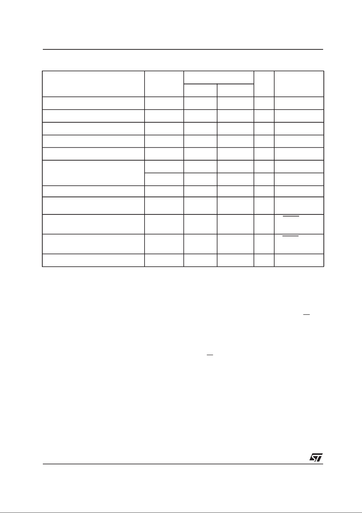
ST10F163
32/58
Read/Write active current
4
I
RWL
6)
-500 – µAV
OUT=VOLmax
ALE inactive current
4
I
ALEL
5
40 – µAV
OUT=VOLmax
ALE active current
4
I
ALEH
6
– 500 µAV
OUT
= 2.4 V
Port 6 inactive current
4
I
P6H
5
– -40 µAV
OUT
= 2.4 V
Port 6 active current
4
I
P6L
6
-500 – µAV
OUT=VOL1max
PORT0 configuration current
4
I
P0H
5
– -10 µAVIN=V
IHmin
I
P0L
6
-100 – µAVIN=V
ILmax
XTAL1 input current I
IL
CC – ±20 µA0V<VIN<V
DD
Pin capacitance4(digital inputs/outputs)
C
IO
CC – 10 pF f = 1 MHz
T
A
=25°C
Power supply current I
CC
–20+
3.5 * f
CPU
mA RSTIN =V
IL2
f
CPU
in [MHz]
7)
Idle mode supply current I
ID
–10+
1.2 * f
CPU
mA RSTIN = V
IH1
f
CPU
in [MHz]
8)
Power-down mode supply current
I
PD
–50µA
V
DD
= 5.5 V
9)
1. ST10F163 pins are equipped with Low-Noise output drivers, which significantly improve the device’s EMI performance. These Low-Noise
drivers deliver their maximum current onlyuntil the respective target output level is reached. After that, the output current isreduced. This
results in an increasedimpedance of the driver, which attenuates electrical noise from the connected PCB tracks. The current specified in
column “Test Conditions” is delivered in anycase.
2. This specification is not validfor outputs which are switched toopen drain mode. In this case the respective output will floatand the voltage
results from the external circuitry.
3. Not 100% tested, guaranteed by design characterization.
4. This specification is only validduring Reset, or during Hold- or Adapt-mode. Port 6 pins are only affected, if they are used for CS output
and the open drain function isnot enabled.
5. The maximum current may be drawn while the respective signalline remains inactive.
6. The minimum current must be drawn in order todrive the respective signal line active.
7. The power supply current is a function of the operating frequency. This dependency is illustrated in the figure below. These parameters
are tested at V
DDmax
and 25MHz CPUclock with all outputs disconnected and all inputs at VILor VIH. The chip is configured with a demux
16-bit bus, direct clock drive, 5 chip select lines and 2 segment address lines, EA pin islow during reset. After reset, Port0 is driven with
the value‘00CCh’ that produces infinite execution ofNOP instructionwith 15wait-state, R/W delay, memory tristatewaitstate, normalALE.
Peripherals are not activated.
8. Idle mode supply current is a function of the operating frequency. This dependency is illustrated in thefigure below. These parametersare
tested at V
DDmax
and 25 MHz CPUclock with all outputs disconnected and all inputs at VILor VIH.
9. This parameter is tested including leakage currents. All inputs (including pins configured asinputs) at0 Vto 0.1 Vor at V
DD
– 0.1 V toVDD,
V
REF
= 0 V, all outputs (including pins configured as outputs) disconnected.
Table 15 : DC Characteristics (continued)
Parameter Symbol
Limit Values
Unit Test Condition
min. max.

ST10F163
33/58
XVI.4 - AC characteristics
XVI.4.1 - Testwaveforms
Figure 8 : Supply/idle current as a function of operating frequency
I [mA]
f
CPU
[MHz]
5
10
15 20
100
50
10
I
IDmax
I
CCmax
25
Figure 9 : Input/output waveforms
Figure 10 : Float waveforms
2.4V
0.45V
Test Points
0.2V
DD
+0.9
0.2V
DD
+0.9
0.2V
DD
-0.1
0.2V
DD
-0.1
AC inputs during testing aredriven at 2.4 V for alogic ‘1’ and 0.4 V fora logic ‘0’.
Timingmeasurements are madeat VIH min for a logic‘1’ and VIL max for a logic ‘0’.
For timing purposes a port pin isno longer floatingwhen a 100mV change from load voltageoccurs,
but begins to float when a 100 mV change from the loaded VOH/VOLlevel occurs(IOH/IOL= 20 mA).
Timing
Reference
Points
V
Load
+0.1V
V
Load
-0.1V
V
OH
-0.1V
V
OL
+0.1V
V
Load
V
OL
V
OH

ST10F163
34/58
XVI.4.2 - Definition of internal timing
The internal operation of the ST10F163 is controlled by the internalCPU clock f
CPU
. Both edges
of the CPU clock can trigger internal (e.g. pipeline) or external (e.g. bus cycles) operations.
The specification of the external timing (AC Characteristics) therefore depends on the time
between two consecutiveedges ofthe CPU clock,
called “TCL” (see figure below).
The CPU clock signal can be generated by different mechanisms. The duration of TCLs and their
variation (and also the derived external timing)
depends on the used mechanism to generate
f
CPU
. This influence must be regarded when cal-
culating the timings forthe ST10F163.
The example for PLL operation shown in the fig-
ure above refers to a PLL factor of 4. The mechanism used to generate the CPU clock is selected
during reset by the logic levels on pins P0.15-13
(P0H.7-5).
XVI.4.3 - Clock generation modes
The table below associatesthe combinations of these threebits with the respective clock generationmode.
Figure 11 : Generation mechanisms for the CPU clock
P0.15-13
(P0H.7-5)
CPU Frequency
f
CPU=fXTAL
*F
External Clock Input
Range
1)
1. The external clock input range refers to a CPU clock range of 1...25 MHz.
Notes
111 F
XTAL
* 4 2.5 to 6.25 MHz
Default configuration
110 F
XTAL
* 3 3.33 to 8.33 MHz
101 F
XTAL
*2 5to12.5MHz
100 F
XTAL
* 5 2 to 5 MHz
011 F
XTAL
* 1 1 to 25 MHz
Direct drive
2)
2. The maximum depends on the duty cycle of the external clock signal.
010 F
XTAL
* 1.5 6.66 to 16.6 MHz
001 F
XTAL
/ 2 2 to 50 MHz
CPU clock via prescaler
3)
3. The maximum input frequency is 25 MHz when usingan external crystal with the internaloscillator; providingthat internalserial resistance
of thecrystal is less than 40 Ω. However, higher frequency can be applied withan external clock source, but inthis case, the input clock
signal must reach the defined levels V
IL
andV
IH2.
000 F
XTAL
* 2.5 4 to 10 MHz
TCLTCL
f
CPU
f
XTAL
f
CPU
f
XTAL
Phaselockedloop operation
DirectClockDrive
TCL TCL
f
CPU
f
XTAL
PrescalerOperation
TCLTCL

ST10F163
35/58
XVI.4.4 - Prescaler operation
When pins P0.15-13 (P0H.7-5) equal ’001’ during
reset, the CPU clock is derived from the internal
oscillator (input clock signal) by a2:1 prescaler.
The frequency of f
CPU
is half the frequency of
f
XTAL
and the high and low time of f
CPU
(i.e. the
duration of an individual TCL) is defined by the
period of the input clock f
XTAL
.
The timings listed in the AC Characteristics that
refer to TCLs therefore can be calculated using
the period of f
XTAL
for any TCL.
Note that if the bit OWDDIS in SYSCON register
is cleared, the PLL is running on its free-running
frequency and delivers the clock signal for the
Oscillator Watchdog. If bit OWDDIS is set, then
the PLL is switched off.
XVI.4.5 - Direct drive
When pins P0.15-13 (P0H.7-5) equal’011’ during
reset the on-chip phase locked loop is disabled
and theCPU clock isdirectly driven fromthe internal oscillator with the input clock signal.
The frequency of f
CPU
directly follows the fre-
quency of f
XTAL
so the high and low time of f
CPU
(i.e. the duration of an individual TCL) is defined
by the duty cycle of the input clock f
XTAL
.
The timings listed below that refer to TCLs therefore must be calculated using the minimum TCL
that is possible under the respective circumstances. This minimum value can be calculated
by the following formula:
For two consecutive TCLs the deviation caused
by the duty cycle of f
XTAL
is compensated so the
duration of 2TCL is always 1/f
XTAL
. The minimum
value TCL
min
therefore has to be used only once
for timings that require an odd number of TCLs
(1,3,...). Timings that require an even number of
TCLs (2,4,...) may use theformula:
Note The address float timings in Multiplexed bus mode (t11and
t
45
) use the maximum duration of TCL (TCL
max
= 1/f
XTAL
*
DC
max
) instead of TCL
min
.
If bit OWDDIS in the SYSCON registeris cleared,
the PLL runs on its free-running frequency and
delivers the clock signal for the Oscillator Watch-
dog. If bit OWDDIS is set, then the PLL is
switched off.
XVI.4.6 - Oscillator Watchdog(OWD)
When the clock option selected is direct drive or
direct drive withprescaler, in order to provide afail
safe mechanism in case of a loss of the external
clock, an oscillator watchdog is implemented as
an additional functionality of the PLLcircuitry. This
oscillator watchdog operates as follows:
After a reset, the Oscillator Watchdog is enabled
by default. To disable the OWD, the bit OWDDIS
(bit 4 of SYSCON register)must be set.
When the OWD is enabled, the PLL is running on
its free-running frequency, and increment the
Oscillator Watchdog counter. On each transition of
XTAL1 pin, the Oscillator Watchdog is cleared. If
an external clock failure occurs, thenthe Oscillator
Watchdog counter overflows (after 16 PLL clock
cycles). The CPU clock signal will be switched to
the PLL free-running clock signal, and the Oscillator Watchdog Interrupt Request (XP3INT) is
flagged. The CPU clock will not switch back to the
external clock even if a valid external clock exits
on XTAL1 pin. Only a hardware reset can switch
the CPU clock source back to direct clock input.
When the OWD is disabled, the CPU clock is
always fed from theoscillator input and the PLL is
switched off to decrease power supply current.
XVI.4.7 - Phase locked loop
For all other combinations of pins P0.15-13
(P0H.7-5) during reset the on-chip phase locked
loop is enabled and provides the CPU clock (see
table above). The PLL multiplies the input frequency by the factor F which is selected via the
combination of pins P0.15-13 (i.e. f
CPU=fXTAL
*
F). With every F’th transition of f
XTAL
the PLL circuit synchronizes the CPU clock to the input
clock. This synchronization is done smoothly, i.e.
the CPU clock frequency does not change
abruptly.
Due to this adaptation to the input clock the frequency of f
CPU
is constantly adjusted so it is
locked to f
XTAL
. The slight variation causes a jitter
of f
CPU
which also effects the duration of individ-
ual TCLs.
The timings listed in the AC Characteristics that
refer to TCLs therefore must be calculated using
the minimum TCL that is possible under the
respective circumstances.
TCL
min
1f⁄
XTAL
*DC
min
=
DC duty cycle=
2TC L 1 f
XTAL
⁄=

ST10F163
36/58
The actual minimum value for TCL depends on
the jitter of the PLL. As the PLL is constantly
adjusting its output frequency so it corresponds to
the applied input frequency (crystal or oscillator)
the relative deviation for periods of more than one
TCL is lower than for one single TCL (see formula
and figure below).
For a period ofN* TCL the minimum value is
computed using the corresponding deviation DN:
whereN=number of consecutive TCLs and 1 ≤ N
≤ 40. So for a period of 3TCLs (N = 3):
This is especially important for bus cycles using
waitstates and e.g. for the operation of timers,
serial interfaces, etc. For all sloweroperations and
longer periods (e.g. pulse traingeneration ormeasurement, lower baudrates, etc.) the deviation
caused by the PLL jitter is negligible (see
Figure 12).
XVI.4.8 - Memory cycle variables
The tables below use three variables which are
derived from the BUSCONx registers and represent the special characteristics of the programmed memory cycle. The following table
describes, how these variables are to be computed.
TCL
min
TCL
NOM
*1 lDNl 100⁄ )–(=
D
N
4 N 15) %[]⁄–(±=
D34315⁄–=
3.8%=
3TCL
min
3TCL
NOM
1 3.8 100⁄–()×=
TCL
NOM
0.962×=
57.72nsec@f
CPU
25MHz=()
Description Symbol Values
ALE Extension t
A
TCL * <ALECTL>
Memory Cycle Time Waitstates t
C
2TCL * (15 - <MCTC>)
Memory Tristate Time t
F
2TCL * (1 - <MTTC>)
Figure 12 : Approximated maximum PLLjitter
3216
8
42
±1
±2
±3
±4
Max.jitter [%]
N
This approximated formula is valid for
1 < N < 40 and10MHz < fCPU < 25MHz.

ST10F163
37/58
XVI.4.9 - External clock drive XTAL1
VDD=5V±10% VSS=0V TA= 0 to+70 °C
Parameter Symbol
f
CPU=fXTAL
f
CPU=fXTAL
/2
f
CPU=fXTAL
*N
N = 1.5/2,/2.5/3/4/5
Unit
min max min max min max
Oscillator period t
OSC
SR
40
1)
1000 20 500 40 * N 100 * N ns
High time t
1
SR
18
2)
–
6
2)
–
10
2)
–ns
Low time t
2
SR
18
2)
–
6
2)
–
10
2)
–ns
Rise time t
3
SR –
10
2)
–
6
3)
–
10
2)
ns
Fall time t
4
SR –
10
2)
–
6
2)
–
10
2)
ns
1. Theoretical minimum. The real minimum value depends on the duty cycle of the input clock signal.
2. The input clock signal must reach the defined levels VIL and VIH2.
Figure 13 : External clock drive XTAL1
t
1
t
3
t
4
V
IL
t
2
t
OSC
V
IH2

ST10F163
38/58
XVI.4.10 - Multiplexed bus
VDD=5V±10% VSS=0V TA= 0 to+70°CC
L
= 100 pF
ALE cycle time = 6 TCL + 2tA+tC+tF(120 ns at 25-MHz CPU clock without waitstates)
Table 16 : Multiplexed bus characteristics
Parameter Symbol
Max. CPU Clock
25 MHz
Variable CPU Clock
1/2TCL = 1 to 25MHz
Unit
min. max. min. max.
ALE high time t
5
CC 10 +t
A
– TCL - 10
+t
A
–ns
Address setup to ALE t
6
CC 4 + t
A
– TCL -
16+ t
A
–ns
Address hold after ALE t
7
CC 10 +t
A
– TCL - 10
+t
A
–ns
ALE falling edge toRD, WR (with RW-delay) t
8
CC 10 +t
A
– TCL - 10
+t
A
–ns
ALE falling edge toRD, WR (no RW-delay) t
9
CC -10 + t
A
– -10 + t
A
–ns
Address float after RD, WR(with RW-delay) t
10
CC–6–6ns
Address float after RD, WR(no RW-delay) t
11
CC – 26 – TCL + 6 ns
RD, WR low time (with RW-delay) t
12
CC 30 + t
C
– 2TCL - 10
+t
C
–ns
RD, WR low time (no RW-delay) t
13
CC 50 + t
C
– 3TCL - 10
+t
C
–ns
RD to valid data in (with RW-delay) t
14
SR – 20 + t
C
– 2TCL - 20
+t
C
ns
RD to valid data in (no RW-delay) t
15
SR – 40 + t
C
– 3TCL - 20
+t
C
ns
ALE low to valid data in t
16
SR – 40
+t
A+tC
– 3TCL - 20
+t
A+tC
ns
Address/Unlatched CS to valid data in t
17
SR – 50+2tA+
t
C
– 4TCL - 30
+2t
A+tC
ns
Data hold after RD rising edge t
18
SR0–0–ns
Data float after RD t
19
SR – 26 + t
F
– 2TCL - 14
+t
F
ns
Data valid to WR t
22
CC 20 + t
C
– 2TCL - 20
+t
C
–ns
Data hold after WR t
23
CC 26 + t
F
– 2TCL - 14
+t
F
–ns
ALE rising edge after RD, WR t
25
CC 26 + t
F
– 2TCL - 14
+t
F
–ns
Address/Unlatched CS hold after RD, WR t
27
CC 26 + t
F
– 2TCL - 14
+t
F
–ns
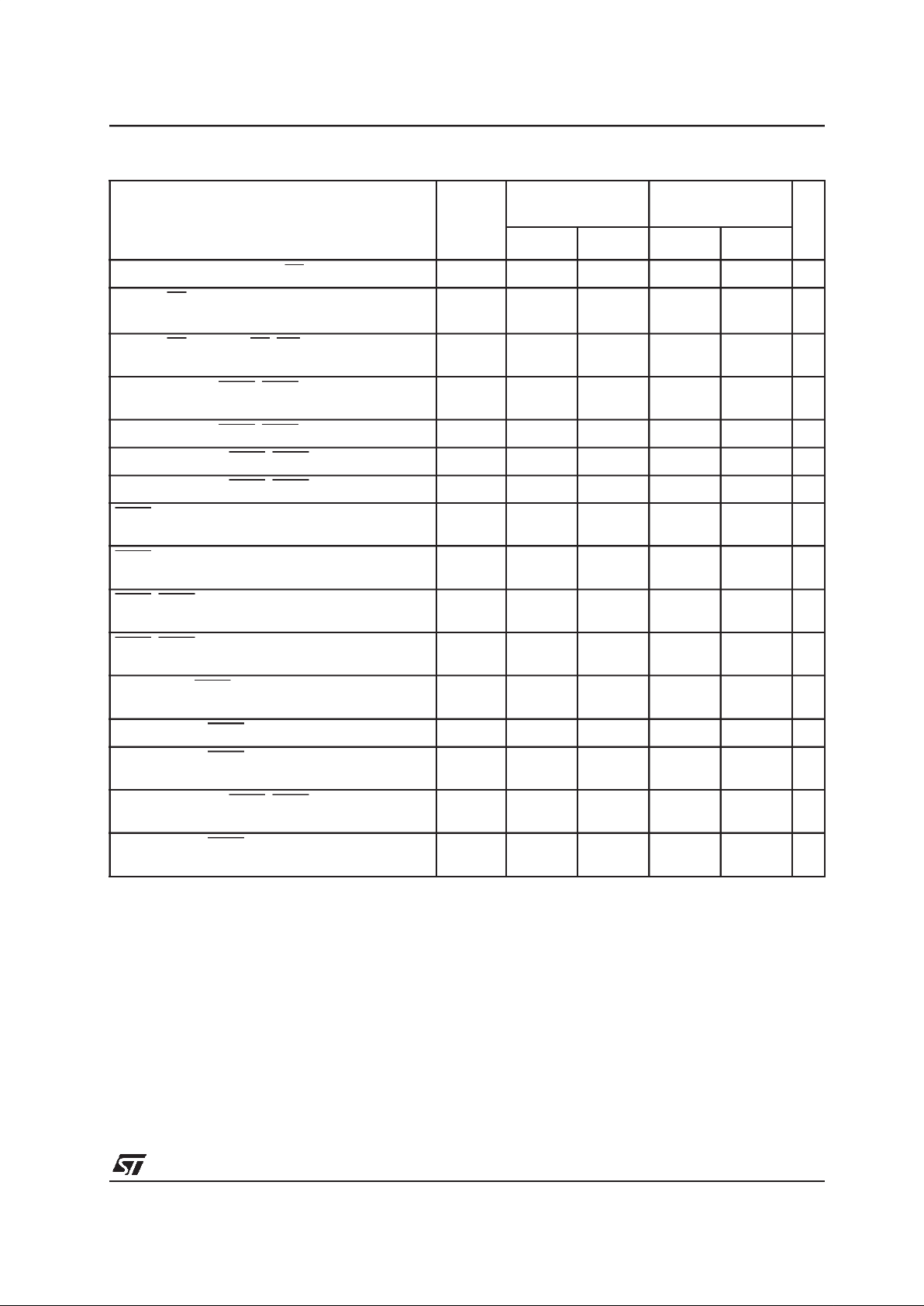
ST10F163
39/58
ALE falling edge toLatched CS t
38
CC -4 - t
A
10 - t
A
-4 - t
A
10 - t
A
ns
Latched CS low to Valid Data In t
39
SR – 40+ tC+
2t
A
– 3TCL - 20
+t
C
+2t
A
ns
Latched CS hold after RD, WR t
40
CC 46 + t
F
– 3TCL - 14
+t
F
–ns
ALE fall. edge to RdCS, WrCS (with RW delay) t
42
CC 16 +t
A
– TCL -4 +
t
A
–ns
ALE fall. edge to RdCS, WrCS (no RW delay) t
43
CC -4 + t
A
–-4+t
A
–ns
Address float after RdCS, WrCS (with RW delay) t
44
CC–0–0ns
Address float after RdCS, WrCS (no RW delay) t
45
CC – 20 – TCL ns
RdCS to Valid Data In (with RW delay) t
46
SR – 16 + t
C
– 2TCL - 24
+t
C
ns
RdCS to Valid Data In (no RW delay) t
47
SR – 36 + t
C
– 3TCL - 24
+t
C
ns
RdCS, WrCS Low Time (with RW delay) t
48
CC 30 + t
C
– 2TCL - 10
+t
C
–ns
RdCS, WrCS Low Time (no RW delay) t
49
CC 50 + t
C
– 3TCL - 10
+t
C
–ns
Data valid to WrCS t
50
CC 26 + t
C
–2TCL-
14+ t
C
–ns
Data hold after RdCS t
51
SR0–0–ns
Data float after RdCS t
52
SR – 20 + t
F
– 2TCL - 20
+t
F
ns
Address hold after RdCS, WrCS t
54
CC 20 + t
F
– 2TCL - 20
+t
F
–ns
Data hold after WrCS t
56
CC 20 + t
F
– 2TCL - 20
+t
F
–ns
Table 16 : Multiplexed bus characteristics (continued)
Parameter Symbol
Max. CPU Clock
25 MHz
Variable CPU Clock
1/2TCL = 1 to 25MHz
Unit
min. max. min. max.
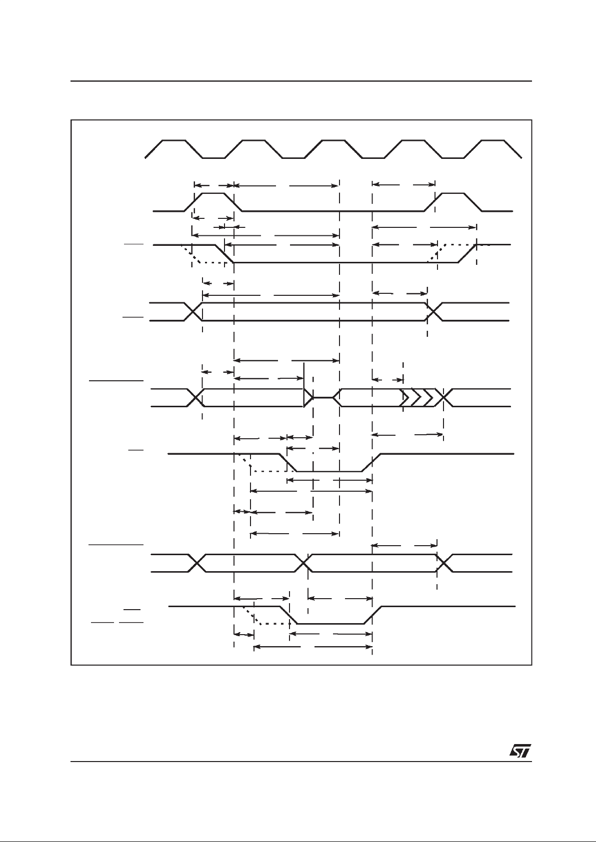
ST10F163
40/58
Figure 14 : External Memory Cycle: multiplexed bus, with/without read/write delay, normal ALE
Data In
Data OutAddress
Address
t
38
t
10
ALE
CSx
BUS
P0
Read Cycle
RD
BUS
P0
Write Cycle
WR,
WRL, WRH
t
5
t
16
t
39
t
40
t
25
t
27
t
18
t
14
t
22
t
23
t
12
t
8
t
8
t
6m
t
19
CLKOUT
Address
A23-A16
(A15-A8)
BHE
t
17
t
6
t
7
t
9
t
11
t
13
t
15
t
16
t
12
t
13
Address
t
9
t
17
t
6
t
27
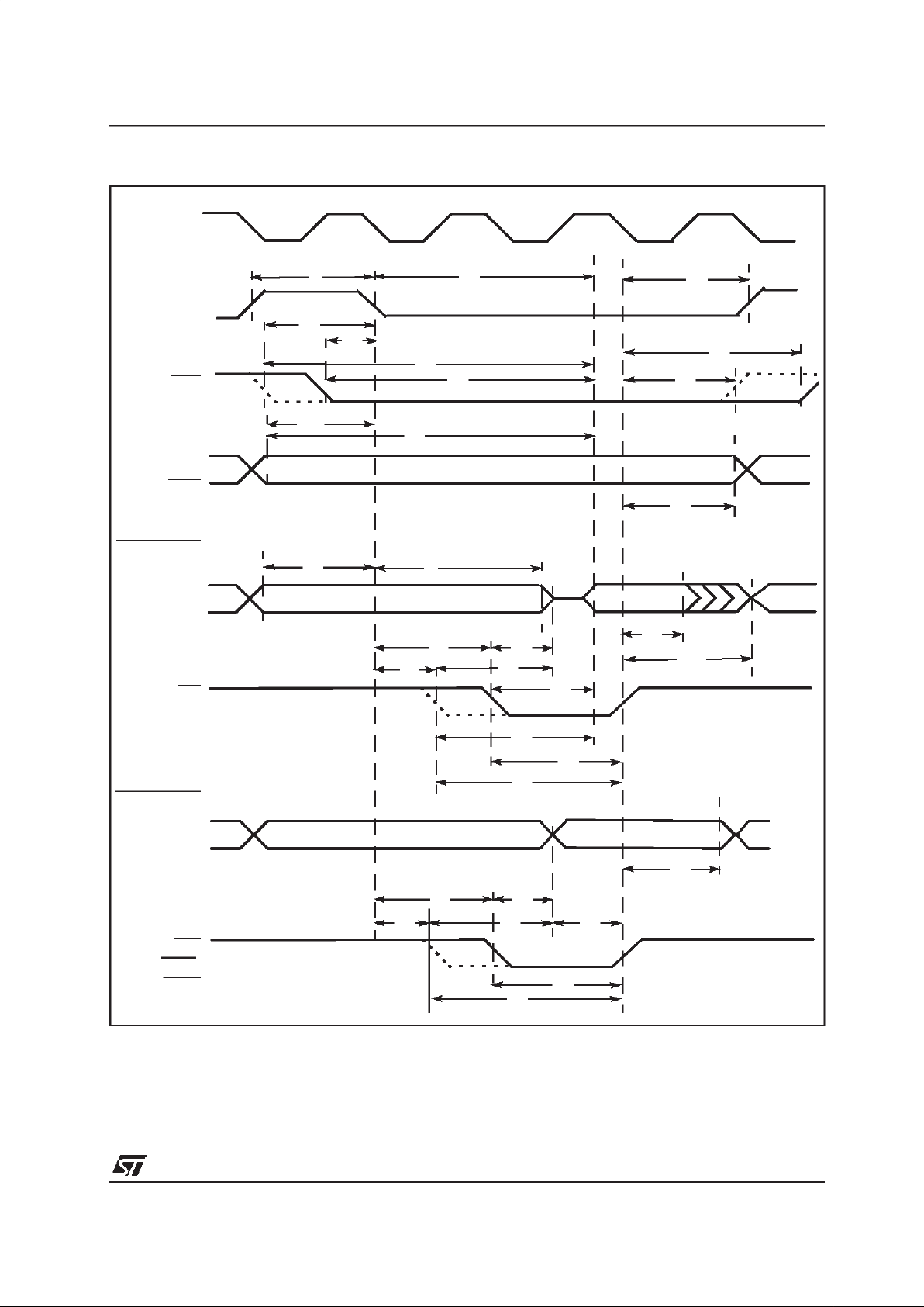
ST10F163
41/58
Figure 15 : External Memory Cycle: multiplexed bus, with/without read/write delay, extended ALE
Data Out
Address
Data InAddress
Address
ALE
RD
Write Cycle
WR
WRL,
WRH
t
5
t
16
t
6
t
7
t
39
t
40
t
14
t
8
t
18
t
23
t
6
Read Cycle
t
27
BUS
P0
BUS
P0
t
38
t
10
t
19
CSx
CLKOUT
t
25
t
17
t
9
t
11
t
15
t
12
t
13
t
8
t
10
t
9
t
11
t
12
t
13
t
22
A23-A16
(A15-A8)
BHE
t
27
t
17
t
6

ST10F163
42/58
Figure 16 : External Memory Cycle: multiplexed bus, with/without read/write delay, normal ale, read/
write chip select
Data In
Data OutAddress
Address
t
44
ALE
BUS
P0
Read Cycle
RdCSx
BUS
P0
Write Cycle
WrCSx
t
5
t
16
t
25
t
27
t
51
t
46
t
50
t
56
t
48
t
42
t
42
t
6
t
52
CLKOUT
Address
A23-A16
(A15-A8)
BHE
t
17
t
6
t
7
t
43
t
45
t
49
t
47
t
16
t
48
t
49
Address
t
43
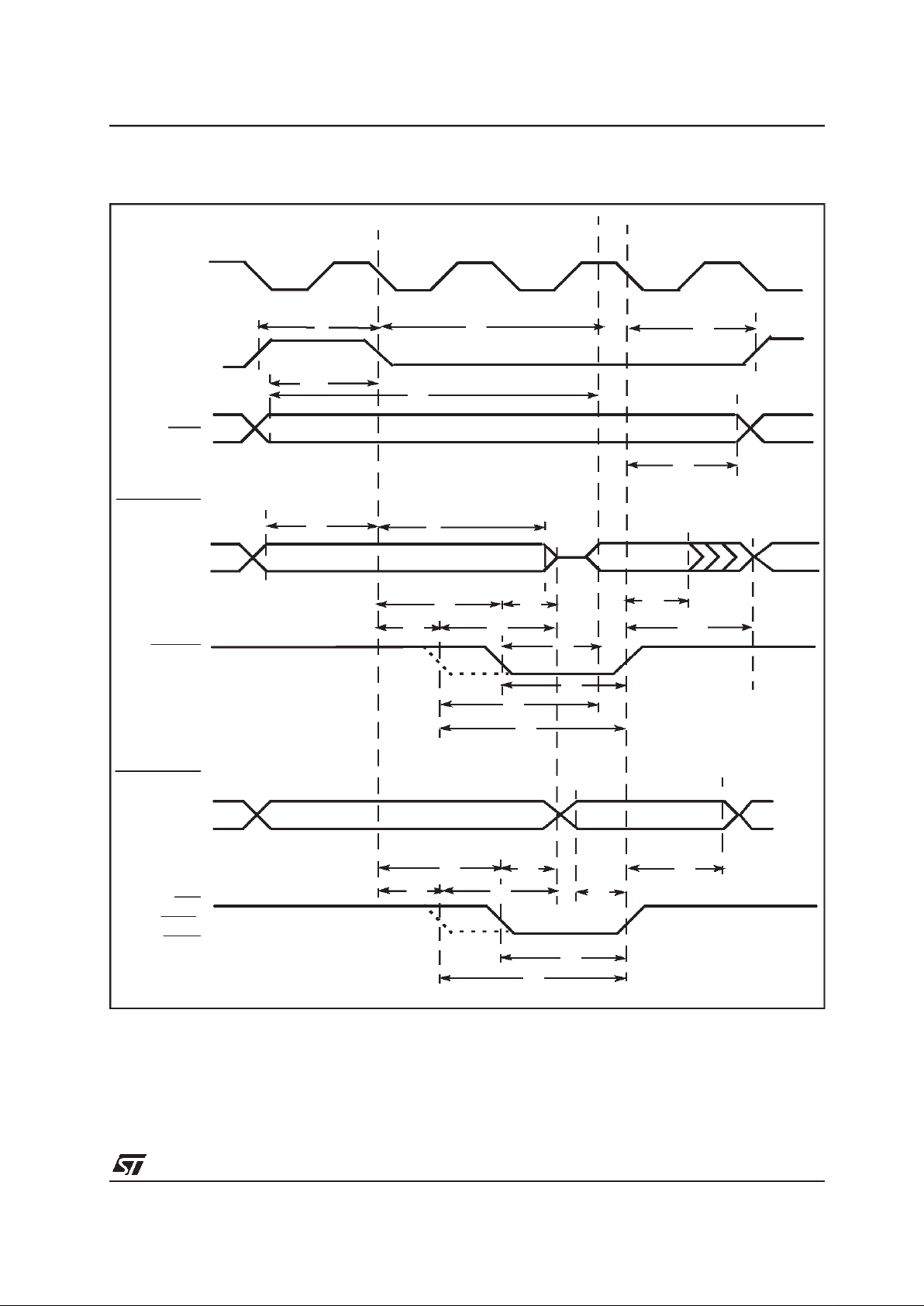
ST10F163
43/58
Figure 17 : External Memory Cycle: multiplexed bus, with/without read/write delay, extended ale, read/
write chip select
Data OutAddress
Data In
Address
Address
ALE
RdCSx
Write Cycle
WR
WRL,
WRH
t
5
t
16
t
6
t
7
t
46
t
42
t
42
t
50
t
18
t
56
t
6
Read Cycle
t
54
BUS
P0
BUS
P0
t
44
t
19
A23-A16
(A15-A8)
BHE
CLKOUT
t
25
t
17
t
43
t
45
t
47
t
48
t
49
t
49
t
43
t
48
t
44
t
45

ST10F163
44/58
XVI.4.11 - Demultiplexed bus
VDD=5V±10% VSS=0V TA= 0 to +70 °CC
L
= 100 pF
ALE cycle time = 4 TCL + 2tA+tC+tF(80 ns at 25 MHz CPU clock without waitstates)
Table 17 : Demultiplexed bus characteristics
Parameter Symbol
Max. CPU Clock
= 25MHz
Variable CPU Clock
1/2TCL = 1 to 25MHz
Unit
min. max. min. max.
ALE high time t
5
CC 10 + t
A
– TCL -
10+ t
A
–ns
Address setup to ALE t
6
CC 4 + t
A
– TCL -
16+ t
A
–ns
Address/Unlatched CS setup to RD, WR
(with RW-delay)
t
80
CC 30 +2t
A
– 2TCL -10
+2t
A
–ns
Address/Unlatched CS setup to RD, WR
(no RW-delay)
t
81
CC 10 +2t
A
– TCL -10
+2t
A
–ns
RD, WR lowtime (with RW-delay) t
12
CC 30 + t
C
– 2TCL -10
+t
C
–ns
RD, WR lowtime (no RW-delay) t
13
CC 50 + t
C
– 3TCL -10
+t
C
–ns
RD to valid data in (with RW-delay) t
14
SR – 20 + t
C
– 2TCL -20
+t
C
ns
RD to valid data in (no RW-delay) t
15
SR – 40 + t
C
– 3TCL -20
+t
C
ns
ALE low to valid data in t
16
SR – 40 + tA+
t
C
– 3TCL - 20
+t
A+tC
ns
Address/Unlatched CS to valid data in t
17
SR – 50 +2tA+
t
C
– 4TCL - 30
+2t
A+tC
ns
Data hold after RDrising edge t
18
SR0–0–ns
Data float after RD rising edge (with RW-delay
1)
)
t
20
SR – 26 + t
F
– 2TCL - 14
+t
F
+
2t
A
1)
ns
Data floatafter RD risingedge (no RW-delay1))
t21SR – 10 + t
F
– TCL - 10
+t
F
+
2t
A
1)
ns
Data valid to WR t
22
CC 20 + t
C
– 2TCL- 20
+t
C
–ns
Data hold after WR t
24
CC 10 +t
F
– TCL -
10+ t
F
–ns
ALE rising edge after RD, WR t
26
CC -10 + t
F
–-10+t
F
–ns
Address/Unlatched CS hold after RD, WR
2)
t28CC 0 +t
F
–0+t
F
–ns
ALE falling edge to Latched CS t
38
CC -4 - t
A
10 - t
A
-4 -t
A
10 - t
A
ns

ST10F163
45/58
Latched CS low to Valid Data In t
39
SR – 40 + tC+
2t
A
– 3TCL - 20
+t
C
+2t
A
ns
Latched CS hold after RD, WR t
41
CC 6 +t
F
– TCL - 14
+t
F
–ns
Addresssetup to RdCS, WrCS (with RW-delay) t
82
CC 26 +2t
A
– 2TCL -14
+2t
A
–ns
Address setup to RdCS, WrCS (no RW-delay) t
83
CC 6 + 2t
A
– TCL -14
+2t
A
–ns
RdCS to Valid Data In (with RW-delay) t
46
SR – 16 + t
C
– 2TCL -24
+t
C
ns
RdCS to Valid Data In (no RW-delay) t
47
SR – 36 + t
C
– 3TCL -24
+t
C
ns
RdCS, WrCS Low Time (with RW-delay) t
48
CC 30 + t
C
– 2TCL -10
+t
C
–ns
RdCS, WrCS Low Time (no RW-delay) t
49
CC 50 + t
C
– 3TCL -10
+t
C
–ns
Data valid to WrCS t
50
CC 26 + t
C
– 2TCL -14
+t
C
–ns
Data hold after RdCS t
51
SR0–0–ns
Data float after RdCS (with RW-delay) t
53
SR – 20 + t
F
– 2TCL -20
+t
F
ns
Data float after RdCS (no RW-delay) t
68
SR – 0 + t
F
– TCL - 20
+t
F
ns
Address hold after RdCS, WrCS t
55
CC -10 + t
F
–-10+t
F
–ns
Data hold after WrCS t
57
CC 6 +t
F
– TCL - 14
+t
F
–ns
1. RW-delay and t
A
refer to the following bus cycle.
2. Read data are latched with the same clock edge that triggers the address change and the rising RD edge. Therefore
address changes before the end of RD have no impact on read cycles
Table 17 : Demultiplexed bus characteristics(continued)
Parameter Symbol
Max. CPU Clock
= 25MHz
Variable CPU Clock
1/2TCL = 1 to 25MHz
Unit
min. max. min. max.

ST10F163
46/58
Figure 18 : External Memory Cycle: demultiplexed bus, with/without read/write delay, normal ALE
Data In
Data Out
t
38
ALE
CSx
P0 BUS
(D15-D8)
D7-D0
Read Cycle
RD
P0 BUS
(D15-D8)
D7-D0
Write Cycle
WR(L),
WRH
t
5
t
16
t
39
t
41
t
18
t
14
t
22
t
12
CLKOUT
Address
A23-A16
(A15-A8)
BHE
t
17
t
13
t
15
t
12
t
13
t
21
t
20
t
81
t
80
t
26
t
24
t
17
t
6
t
41u
t
6
t
80
t
81
t
28
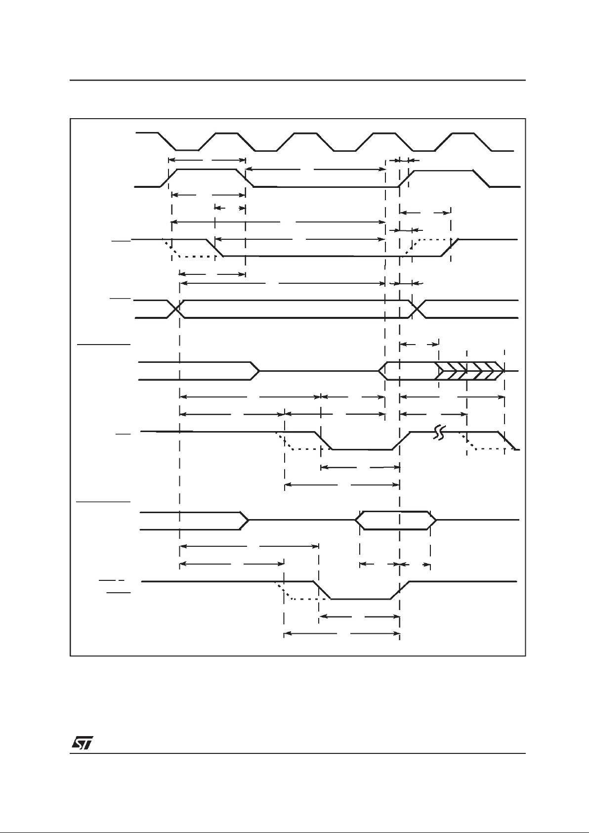
ST10F163
47/58
Figure 19 : External Memory Cycle: demultiplexed bus, with/without read/write delay, extended ALE
Address
ALE
RD
Write Cycle
WR(L),
WRH
t
5
t
16
t
39
t
41
t
14
t
24
t
6
t
38
t
20
CSx
CLKOUT
t
26
t
17
t
15
t
12
t
13
t
12
t
13
t
22
A23-A16
(A15-A8)
BHE
Data In
P0 BUS
(D15-D8)
D7-D0
Read Cycle
t
18
t
21
t
6
t
17
t
28
t
28
Data Out
t
80
t
81
t
80
t
81
P0 BUS
(D15-D8)
D7-D0

ST10F163
48/58
Figure 20 : External Memory Cycle: demultiplexed bus, with/without read/write delay, normal ale, read/
write chip select
Data In
Data Out
ALE
P0 BUS
(D15-D8)
D7-D0
Read Cycle
RdCsx
P0 BUS
(D15-D8)
D7-D0
Write Cycle
WrCSx
t
5
t
16
t
51
t
46
t
50
t
48
CLKOUT
Address
A23-A16
(A15-A8)
BHE
t
17
t
49
t
47
t
48
t
49
t
68
t
53
t
83
t
82
t
26
t
57
t
55
t
6
t
82
t
83

ST10F163
49/58
Figure 21 : External Memory Cycle: demultiplexed bus, no read/write delay,extended ale, read/write
chip select
Address
ALE
RdCSx
Write Cycle
WrCSx
t
5
t
16
t
46
t
57
t
6
t
53
CLKOUT
t
26
t
17
t
47
t
48
t
49
t
48
t
49
t
50
A23-A16
(A15-A8)
BHE
Data In
P0 BUS
(D15-D8)
D7-D0
Read Cycle
t
51
t
68
t
55
Data Out
t
82
t
83
t
82
t
83
P0 BUS
(D15-D8)
D7-D0
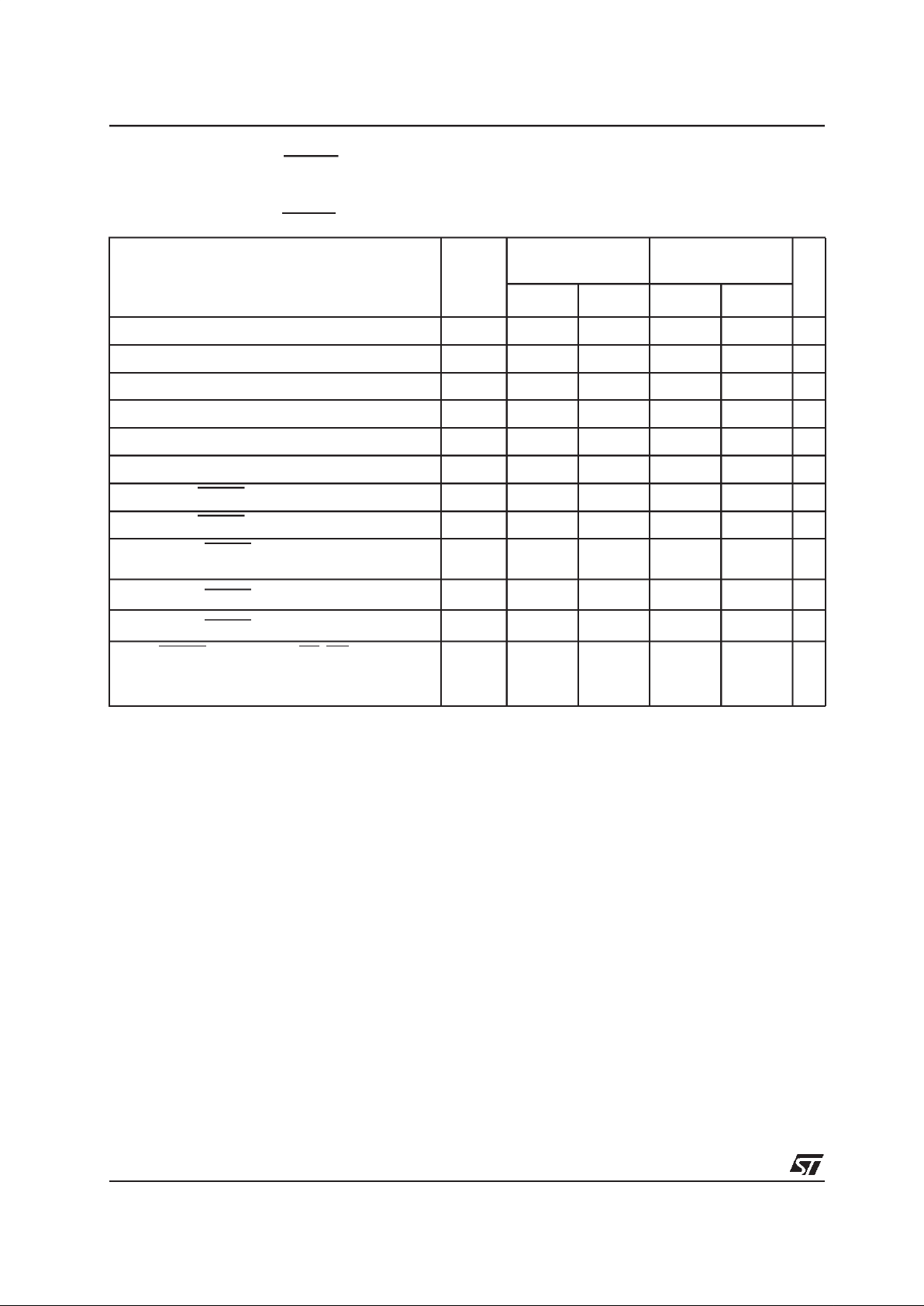
ST10F163
50/58
XVI.4.12 - CLKOUT and READY
VDD=5V±10% VSS=0V TA= 0 to +70°CC
L
= 100 pF
Table 18 : CLKOUT and READY characteristics
Parameter Symbol
Max. CPU Clock
= 25MHz
Variable CPU Clock
1/2TCL = 1 to 25MHz
Unit
min. max. min. max.
CLKOUT cycle time t
29
CC 40 40 2TCL 2TCL ns
CLKOUT high time t
30
CC 14 – TCL – 6 – ns
CLKOUT low time t
31
CC 10 – TCL – 10 – ns
CLKOUT rise time t
32
CC–4–4ns
CLKOUT fall time t
33
CC–4–4ns
CLKOUT rising edge to ALE falling edge t
34
CC 0 +t
A
10 + t
A
0+t
A
10 +t
A
ns
Synchronous READY setup time to CLKOUT t
35
SR14–14–ns
Synchronous READY hold time after CLKOUT t
36
SR4–4–ns
Asynchronous READY low time t
37
SR 58 – 2TCL +
18
–ns
Asynchronous READY setup time
1)
t58SR14–14–ns
Asynchronous READY hold time
1)
t59SR4–4–ns
Async. READY hold time after RD, WR high
(Demultiplexed Bus)
2)
t60SR 0 0 + 2tA+
t
C+tF
2)
0 TCL - 20
+2t
A+tC
+t
F
2)
ns
1. These timings are given for test purposes only, in order to assure recognition at a specific clock edge.
2. Demultiplexed bus is the worst case. For multiplexed bus 2TCL are to be added to the maximum values. This adds
even more time for deactivating READY.
The2t
A
and tCrefer to the next following bus cycle, tFrefers to thecurrent bus cycle

ST10F163
51/58
1. Cycle as programmed, including MCTC waitstates (Example shows 0 MCTC WS).
2. The leading edge of the respective command depends on RW-delay.
3. READY sampled HIGH at this sampling point generates a READY controlled waitstate, READY sampled LOW at this sampling point terminates thecurrently running bus cycle.
4. READY may be deactivated in response to the trailing (rising) edge of the corresponding command (RDor WR).
5. If the Asynchronous READY signal does not fulfill the indicated setupand hold times with respect to CLKOUT (e.g. because CLKOUT is
not enabled), it must fulfill
t
37 in order to be safely synchronized. This is guaranteed, if READY is removed in response to the command
(see Note 4)).
6. Multiplexed bus modes have a MUX waitstate added after a bus cycle, and an additional MTTC waitstate may be inserted here.
For a multiplexed bus with MTTC waitstate this delay is 2 CLKOUT cycles, for a demultiplexed bus without MTTC waitstate this delay is
zero.
7. The next externalbus cycle may start here.
Figure 22 : CLKOUT and READY
CLKOUT
ALE
t
30
t
34
Sync
READY
t
35
t
36
t
35
t
36
Async
READY
t
58
t
59
t
58
t
59
waitstate
READY
MUX/Tristate 6)
t
32
t
33
t
29
Running cycle 1)
t
31
t
37
3)
3)
5)
Command
RD, WR
t
60
4)
see 6)
2)
7)
3)
3)

ST10F163
52/58
XVI.4.13 - External bus arbitration
1. The ST10F163 will complete the currently running bus cycle before granting bus access.
2. This is the first possibility for BREQ to get active.
3. The CS outputs will be resistive high (pullup) after
t
64
.
VDD=5V±10% VSS=0V TA= 0 to +70 °C
CL(for PORT0, PORT1,Port 4, ALE, RD, WR, BHE, CLKOUT) = 100 pF
CL(for Port 6, CS) =100 pF
Parameter Symbol
Max. CPU Clock
= 25MHz
Variable CPU Clock
1/2TCL = 1 to 25MHz
Unit
min. max. min. max.
HOLD input setup time toCLKOUT t
61
SR20–20–ns
CLKOUT to HLDA high or BREQ low delay t
62
CC–20–20ns
CLKOUT to HLDA low or BREQ high delay t
63
CC–20–20ns
CSx release t
64
CC–20–20ns
CSx drive t
65
CC -4 24 -4 24 ns
Other signals release t
66
CC–20–20ns
Other signals drive t
67
CC -4 24 -4 24 ns
Figure 23 : External bus arbitration, releasing the bus
CLKOUT
HOLD
t
61
HLDA
t
63
Other
Signals
t
66
1)
CSx
(On P6.x)
t
64
1)
2)
BREQ
t
62
3)

ST10F163
53/58
Figure 24 : External bus arbitration, (regaining the bus)
1. This is the last chance for BREQ to trigger the indicated regain-sequence.
Even if BREQ is activated earlier, the regain-sequence is initiated by HOLD going high.
Please note that HOLD may also be deactivated without the ST10F163 requesting the bus.
2. The nextST10F163 driven bus cycle may start here.
CLKOUT
HOLD
HLDA
Other
Signals
t
62
CSx
(On P6.x)
t
67
t
62
1)
2)
t
65
t
61
BREQ
t
63
t
62

ST10F163
54/58
XVI.4.14 - Synchronous serial port timing
V
CC
=5V±10% VSS=0V TA= 0 to +70°C CL= 100 pF
Table 19 : Synchronous serial porttiming characteristics
Parameter Symbol
Max. Baudrate
= 12.5 / 10 MBd
Variable Baudrate
= 0.5 to 12.5 MBd
Unit
min. max. min. max.
SSP clock cycle time t
200
CC 80 / 100 80 /100 4 TCL 512 TCL ns
SSP clock high time t
201
CC 30 / 40 – / – t
200
/2 - 10 – ns
SSP clock low time t
202
CC 30 / 40 – / – t
200
/2 - 10 – ns
SSP clock rise time t
203
CC – / – 6 / 6 – 6 ns
SSP clock fall time t
204
CC – / – 6 / 6 – 6 ns
CE active before shift edge t
205
CC 30 / 40 – / – t
200
/2 - 10 – ns
CE inactive after latch edge t
206
CC 70 / 90 90 / 110 t
200
-10 t
200
+10 ns
Write data valid after shift edge t
207
CC – / – 10 / 10 – 10 ns
Write data hold after shift edge t
208
CC 0 / 0 – / – 0 – ns
Write data hold after latch edge t
209
CC 34 / 44 46 / 56 t
200
/2 - 6 t
200
/2 + 6 ns
Read data active after latch edge t
210
SR 50 /60 – / – t
200
/2 + 10 – ns
Read data setup time before latch edge t
211
SR 20 /20 – / – 20 – ns
Read data hold time after latch edge t
212
SR 0 / 0 – / – 0 – ns
Figure 25 : SSP write timing
t
204
t
203
SSPCLK
SSPCEx
SSPDAT
t
205
t
207
t
207
t
207
t
208
t
209
t
206
1st Bit Last Bit2nd Bit
t
200
t
201
t
202
1)
3)
2)
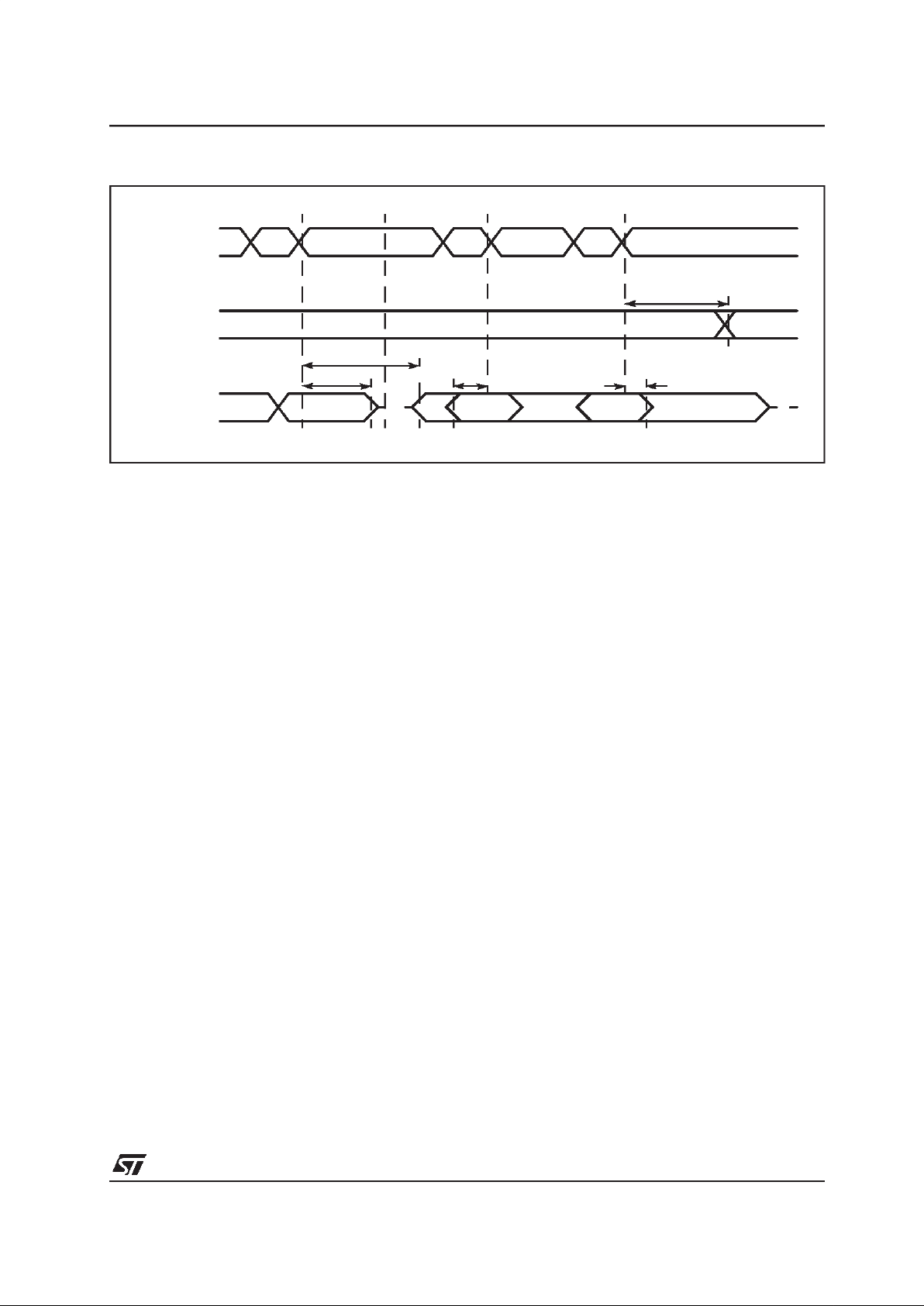
ST10F163
55/58
The transition of shift and latch edge of SSPCLK is programmable. This figure uses the falling edge as shift edge (drawn bold).
The bit timing isrepeated for all bits to be transmitted or received.
The active level of the chip enable lines is programmable. This figure uses an active low CE (drawn bold).
At the end of a transmission orreception the CE signal is disabled in single transfer mode. In continuous transfer mode itremains active.
Figure 26 : SSP read timing
t
211
SSPCLK
SSPCEx
SSPDAT
t
209
t
206
last Wr. Bit
Lst.In Bit
1)
3)
2)
t
212
1st.In Bit
t
210

ST10F163
56/58
XVII - PACKAGE MECHANICAL DATA
XVIII - ORDERING INFORMATION
Figure 27 : Package outline TQFP100 (14 x 14 mm)
Dimensions
Millimeters Inches
Min. Typ. Max. Min. Typ. Max.
A 1.60 0.063
A2 1.35 1.40 1.45 0.053 0.055 0.057
D 15.75 16.00 16.25 0.620 0.630 0.640
D1 13.90 14.00 14.10 0.547 0.551 0.555
D3 12.00 0.472
E 15.75 16.00 16.25 0.620 0.630 0.640
E1 13.90 14.00 14.10 0.547 0.551 0.555
E3 12.00 0.472
e 0.50 0.020
Number of Pins
ND 25
NE 25
N 100
Salestype Temperature range Package
ST10F163BT1 0°Cto70°C TQFP100 (14x 14)
76100
50
D3
e
26
1
25
75
51
c
B
A1
A2
A
D1
D
E3
E1
E
L
K
L1
0,25 mm
.010 inch
GAGE PLANE
0,075 mm
0.03 inch
SEATING PLANE

ST10F163
57/58
XIX - REVISION HISTORY
The following changes have been madefrom ST10F163 Data Sheet revision5 tocreate this revision 6:
Table added Table8 on page 20
Table added Table9 on page 21
Table added Table10 on page 23
Table added Table11 on page 24
Table added Table12 on page 25
Table added Table3 on page 11
Table added Table4 on page 11
Table added Table5 on page 12
Presentation changed Figure 14 to Figure 21
Specification changed t
22
from 2TCL-16+tcto 2TCL-20+t
c
Specification changed t8-t9replaced with t80-t81for demultiplexed bus
Specification changed t
42-t43
replaced with t82-t83for demultiplexed bus
Specification changed t
35
from 10ns to14ns
Specification changed t
36 andt59
from 0ns to 4ns
Specification changed t
37
from ”min 54ns, Var min 2TCL+14ns” to ”min 58ns, Var min 2TCL+18ns”
Specification changed Table15: input hight voltage RSTIN, min. 0.6V
DD
chnaged to 0.7V
DD

ST10F163
58/58
Information furnished is believed to be accurate and reliable. However, STMicroelectronics assumes no responsibility for the
consequences of use of such information nor forany infringement of patents or other rights of third parties which may resultfrom
its use. No license is granted by implication or otherwise under any patent or patent rights of STMicroelectronics. Specifications
mentioned in this publication are subject to change without notice. This publication supersedes and replaces all information
previously supplied. STMicroelectronics products are not authorized for use as critical components in life support devices or
systems without express written approval of STMicroelectronics.
The ST logo is a registered trademark ofSTMicroelectronics
1999 STMicroelectronics - AllRights Reserved
STMicroelectronics GROUP OF COMPANIES
Australia - Brazil - Canada - China - France - Germany - Italy- Japan - Korea - Malaysia - Malta - Mexico - Morocco
The Netherlands - Singapore - Spain - Sweden - Switzerland - Taiwan - Thailand - United Kingdom - U.S.A.
http://www.st.com
 Loading...