

1/65August 1999
■ HIGH PERFORMANCE CPU
– 16-BIT CPU WITH 4-STAGE PIPELINE
– 80ns INSTRUCTION CYCLE TIME @ 25MHz CLK
– 400ns 16 X 16-BIT MULTIPLICATION
– 800ns 32 / 16-BIT DIVISION
– ENHANCED BOOLEAN BIT MANIPULATION
FACILITIES
– ADDITIONAL INSTRUCTIONS TO SUPPORT HLL
AND OPERATING SYSTEMS
– SINGLE-CYCLE CONTEXT SWITCHING SUPPORT
■ MEMORY ORGANIZATION
– 32K BYTE ON-CHIP ROM MEMORY
– UP TO16M BYTE LINEAR ADDRESS SPACE FOR
CODE AND DATA (5M BYTE WITH CAN)
– 2K BYTE ON-CHIP INTERNAL RAM (IRAM)
– 2K BYTE ON-CHIP EXTENSION RAM (XRAM)
■ FAST AND FLEXIBLE BUS
– PROGRAMMABLE EXTERNAL BUS
CHARACTERISTICS FOR DIFFERENT ADDRESS
RANGES
– 8-BIT OR 16-BIT EXTERNAL DATA BUS
– MULTIPLEXED OR DEMULTIPLEXED EXTERNAL
ADDRESS/DATA BUSES
– FIVE PROGRAMMABLE CHIP-SELECT SIGNALS
– HOLD-ACKNOWLEDGE BUS ARBITRATION
SUPPORT
■ INTERRUPT
– 8-CHANNEL PERIPHERAL EVENT CONTROLLER
FOR SINGLE CYCLE, INTERRUPT DRIVEN DATA
TRANSFER
– 16-PRIORITY-LEVEL INTERRUPT SYSTEMWITH
56 SOURCES, SAMPLE-RATE DOWN TO 40ns
■ TIMERS
– TWO MULTI-FUNCTIONAL GENERAL PURPOSE
TIMER UNITS WITH 5 TIMERS
– TWO 16-CHANNEL CAPTURE/COMPARE UNITS
■ A/D CONVERTER
– 16-CHANNEL10-BIT
– 7.76µs CONVERSION TIME
■ FAIL-SAFE PROTECTION
– PROGRAMMABLE WATCHDOG TIMER
– OSCILLATOR WATCHDOG
■ ON-CHIP CAN 2.0B INTERFACE
■ ON-CHIP BOOTSTRAP LOADER
■ CLOCK GENERATION
– ON-CHIP PLL
– DIRECT OR PRESCALEDCLOCK INPUT
■ UP TO 111GENERAL PURPOSE I/O LINES
– INDIVIDUALLY PROGRAMMABLE AS INPUT,
OUTPUT OR SPECIAL FUNCTION
– PROGRAMMABLE DRIVE STRENGTH
– PROGRAMMABLE THRESHOLD (HYSTERESIS)
■ IDLE AND POWER DOWN MODES
– IDLECURRENT <95mA
– POWER-DOWN SUPPLY CURRENT<400µA
■ 4-CHANNEL PWM UNIT
■ SERIAL CHANNELS
– SYNCHRONOUS/ASYNCSERIAL CHANNEL
– HIGH-SPEED SYNCHRONOUS CHANNEL
■ DEVELOPMENT SUPPORT
– C-COMPILERS, MACRO-ASSEMBLER PACKAGES,
EMULATORS, EVAL BOARDS, HLL-DEBUGGERS,
SIMULATORS, LOGIC ANALYZER DISASSEM-
BLERS, PROGRAMMING BOARDS
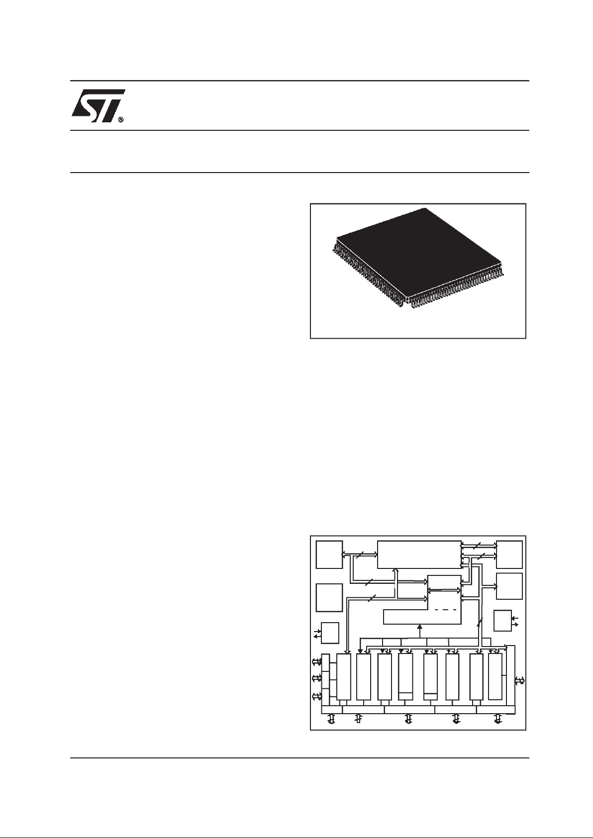
■ 144-PIN PQFP PACKAGE
PQFP144 (28 x 28 mm)
(Plastic Quad Flat Pack)
Port 0Port 1Port 4
Port 6
Port 5
Port 3
Port 2
GPT1
GPT2
ASC usart
BRG
32K
CPU-Core
Internal
RAM
Watchdog
Interrupt Controller
8
815
16
32
16
PEC
16
16
CAN
Port 7
Port 8
External Bus
10-Bit ADC
BRG
SSC
PWM
CAPCOM2
CAPCOM1
8
16
16
OSC.
XRAM
16
Controller
16
8
16
Byte
ROM
ST10C167
16-BIT MCU WITH 32K BYTE ROM
This is advance information on a new product now in development or undergoing evaluation. Details are subject to change without notice.

ST10C167
2/65
TABLE OF CONTENTS Page
I INTRODUCTION......................................................................................................... 4
II PIN DATA .................................................................................................................. 5
III FUNCTIONAL DESCRIPTION.................................................................................... 10
IV MEMORY ORGANIZATION........................................................................................ 11
V CENTRAL PROCESSING UNIT (CPU)...................................................................... 12
VI EXTERNAL BUS CONTROLLER............................................................................... 13
VII INTERRUPT SYSTEM................................................................................................ 14
VIII CAPTURE/COMPARE (CAPCOM) UNIT................................................................... 17
IX GENERAL PURPOSE TIMER UNIT........................................................................... 18
IX.1 GPT1 .......................................................................................................................... 18
IX.2 GPT2 .......................................................................................................................... 19
X PWM MODULE........................................................................................................... 21
XI PARALLEL PORTS.................................................................................................... 22
XII A/D CONVERTER...................................... ................................................................. 23
XIII SERIAL CHANNELS .............................................................................. .................... 24
XIV CAN MODULE............................................................................................................ 26
XV WATCHDOG TIMER................................................................................................... 26
XVI INSTRUCTION SET SUMMARY ............................................................................... . 27
XVII SYSTEM RESET......................................................................................................... 29
XVIII POWER REDUCTION MODES .................................................................................. 30
XIX SPECIAL FUNCTION REGISTER OVERVIEW.......................................................... 31
XIX.1 IDENTIFICATION REGISTERS ............................................................. .................... 37
XX ELECTRICAL CHARACTERISTICS ......................................................................... . 38
XX.1 ABSOLUTE MAXIMUM RATINGS ............................................................................. 38
XX.2 PARAMETER INTERPRETATION ............................................................................. 38
XX.3 DC CHARACTERISTICS ........................................................................................... 39
XX.3.1 A/D converter characteristics ...................................................................................... 40
XX.4 AC CHARACTERISTICS ............................................................................................ 41
XX.4.1 Definition of internal timing ......................................................................................... 42
XX.4.2 Clock generation modes ............................................................................................. 42

ST10C167
3/65
XX.4.3 Prescaler operation .................................................................................................... 43
XX.4.4 Direct drive ................................................................................................................. 43
XX.4.5 Oscillator watchdog (OWD) ........................................................................................ 43
XX.4.6 Phase locked loop ...................................................................................................... 43
XX.4.7 Memory cycle variables .............................................................................................. 44
XX.4.8 External clock drive XTAL1 .......................................... .............................................. 45
XX.4.9 Multiplexed bus ........................................................................................................... 45
XX.4.10 Demultiplexed bus ...................................................................................................... 52
XX.4.11 CLKOUT and READY ................................................................................................. 58
XX.4.12 External bus arbitration ........................................................................... .................... 60
XX.4.13 Highspeed synchronous serial interface (SSC) timing ............................................... 61
XXI PACKAGE MECHANICAL DATA ........................................................................... 64
XXII ORDERING INFORMATION....................................................................................... 64
TABLE OF CONTENTS (continued) Page
ST10C167
4/65
I - INTRODUCTION
The ST10C167 is a derivative of the
STMicroelectronics ST10 family of 16-bit
single-chip CMOS microcontrollers. It combines
high CPU performance (up to 12.5 million
instructions per second) with high peripheral
functionality and enhanced I/O capabilities.
It also provides on-chip high-speed RAM and
clock generation viaPLL.
Figure 1 : Logic Symbol
XTAL1
RSTIN
XTAL2
RSTOUT
NMI
EA
READY
ALE
RD
WR/WRL
Port 5
16-bit
Port 6
8-bit
Port 4
8-bit
Port 3
15-bit
Port 2
16-bit
Port 1
16-bit
Port 0
16-bit
V
DD
V
SS
Port 7
8-bit
Port 8
8-bit
V
AREF
V
AGND
ST10C167
RPD
ST10C167
5/65
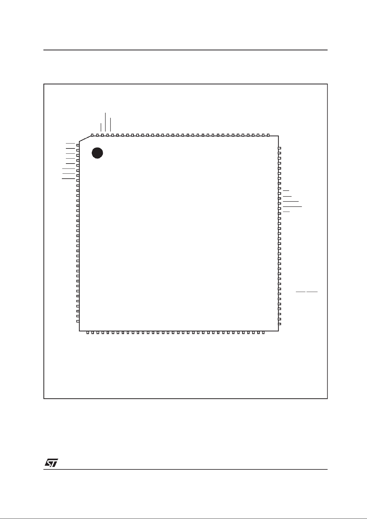
II - PIN DATA
Figure 2 : Pin Configuration (top view)
P6.0/CS0
P6.1/CS1
P6.2/CS2
P6.3/CS3
P6.4/CS4
P6.5/HOLD
P6.6/HLDA
P6.7/BREQ
P8.0/CC16IO
P8.1/CC17IO
P8.2/CC18IO
P8.3/CC19IO
P8.4/CC20IO
P8.6/CC22IO
P8.7/CC23IO
V
DD
V
SS
P7.0/POUT0
P7.1/POUT1
P7.2/POUT2
P7.3/POUT3
P8.5/CC21IO
RPD
P7.4/CC28I0
P7.5/CC29I0
P7.6/CC30I0
P7.7/CC31I0
P5.0/AN0
P5.1/AN1
P5.2/AN2
P5.3/AN3
P5.4/AN4
P5.5/AN5
P5.6/AN6
P5.7/AN7
P5.8/AN8
P5.9/AN9
P0H.0/AD8
P0L.7/AD7
P0L.6/AD6
P0L.5/AD5
P0L.4/AD4
P0L.3/AD3
P0L.2AD2
P0L.A/AD1
P0L.0/AD0
EA
ALE
READY
WR/WRL
RD
V
SS
V
DD
P4.7/A23
P4.6A22/CAN_TxD
P4.5A21/CAN_RxD
P4.4/A20
P4.3/A19
P4.2/A18
P4.1/A17
P4.0/A16
V
SS
V
DD
P3.15/CLKOUT
P3.13/SCLK
P3.12/BHE/WRH
P3.11/RXD0
P3.10/TXD0
P3.9/MTSR
P3.8/MRST
P3.7/T2IN
P3.6/T3IN
V
AREF
V
AGND
P5.10/AN10/T6EUD
P5.11/AN11/T5EUD
P5.12/AN12/T6IN
P5.13/AN13/T5IN
P5.14/AN14/T4EUD
P5.15/AN15/T2EUD
V
SS
V
DD
P2.0/CC0IO
P2.1/CC1IO
P2.2/CC2IO
P2.3/CC3IO
P2.4/CC4IO
P2.5/CC5IO
P2.6/CC6IO
P2.7/CC7IO
V
SS
V
DD
P2.8/CC8IO/EX0IN
P2.9/CC9IO/EX1IN
P2.10/CC10IOEX2IN
P2.11/CC11IOEX3IN
P2.12/CC12IO/EX4IN
P2.13/CC13IO/EX5IN
P2.14/CC14IO/EX6IN
P2.15/CC15IO/EX7IN/T7IN
P3.0/T0IN
P3.1/T6OUT
P3.2/CAPIN
P3.3/T3OUT
P3.4/T3EUD
P3.5/T4IN
V
SS
V
DD
VSSNMI
VDDRSTOUT
RSTIN
VSSXTAL1
XTAL2
VDDP1H.7/A15/CC27IO
P1H.6/A14/CC26IO
P1H.5/A13/CC25IO
P1H.4/A12/CC24IO
P1H.3/A11
P1H.2/A10
P1H.1/A9
P1H.0/A8
VSSVDDP1L.7/A7
P1L.6/A6
P1L.5/A5
P1L.4/A4
P1L.3/A3
P1L.2/A2
P1L.1/A1
P1L.0/A0
P0H.7/AD15
P0H.6/AD14
P0H.5/AD13
P0H.4/AD12
P0H.3/AD11
P0H.2/AD10
P0H.1/AD9
VSSV
DD
1
2
3
4
5
6
7
8
9
10
11
12
13
14
15
16
17
18
19
20
21
22
23
24
25
26
27
28
29
30
31
32
33
34
35
36
3738394041424344454647484950515253545556575859606162636465666768697071
72
108
107
106
105
104
103
102
101
100
99
98
97
96
95
94
93
92
91
90
89
88
87
86
85
84
83
82
81
80
79
78
77
76
75
74
73
144
143
142
141
140
139
138
137
136
135
134
133
132
131
130
129
128
127
126
125
124
123
122
121
120
119
118
117
116
115
114
113
112
111
110
109
ST10C167
ST10C167
6/65
Table 1 : Pin list
Symbol Pin Type Function
P6.0 - P6.7 1 - 8 I/O 8-bit bidirectional I/O port, bit-wise programmable for input or output via
direction bits. Programming an I/O pin as input forces the corresponding
output driver tohigh impedance state. Port 6 outputs can be configured as
push/pull or open drain drivers.
The following Port 6 pins have alternate functions:
1
...
5
6
7
8
O
...
O
I
O
O
P6.0 CS0 Chip Select 0 Output
... ... ...
P6.4 CS4 Chip Select 4 Output
P6.5 HOLD External Master Hold Request Input
P6.6 HLDA Hold Acknowledge Output
P6.7 BREQ Bus Request Output
P8.0 - P8.7 9 - 16 I/O 8-bit bidirectional I/O port, bit-wise programmable for input or output via
direction bits. Programming an I/O pin as input forces the corresponding
output driver tohigh impedance state. Port 8 outputs can be configured as
push/pull or open drain drivers. The input threshold of Port 8 is selectable
(TTL or special).
The following Port 8 pins have alternate functions:
9
...
16
I/O
...
I/O
P8.0 CC16IO CAPCOM2: CC16 Capture Input/Compare Output
... ... ...
P8.7 CC23IO CAPCOM2: CC23 Capture Input/Compare Output
P7.0 - P7.7 19 - 26 I/O 8-bit bidirectional I/O port, bit-wise programmable for input or output via
direction bits. Programming an I/O pin as input forces the corresponding
output driver tohigh impedance state. Port 7 outputs can be configured as
push/pull or open drain drivers. The input threshold of Port 7 is selectable
(TTL or special).
The following Port 7 pins have alternate functions:
19
...
22
23
...
26
O
...
O
I/O
...
I/O
P7.0 POUT0 PWM Channel 0 Output
... ... ...
P7.3 POUT3 PWM Channel 3 Output
P7.4 CC28IO CAPCOM2: CC28 Capture Input/Compare Output
... ... ...
P7.7 CC31IO CAPCOM2: CC31 Capture Input/Compare Output
P5.0 - P5.9
P5.10 - P5.15
27 - 36
39 - 44
I
I
Port 5 is a 16-bit input-only port with Schmitt-Trigger characteristics. The
pins of Port 5 also serve as the (up to 16) analoginput channels for the A/
D converter, where P5.x equals ANx (Analog input channel x), or they
serve as timer inputs:
39
40
41
42
43
44
I
I
I
I
I
I
P5.10 T6EUD GPT2 Timer T6External Up/Down Control Input
P5.11 T5EUD GPT2 Timer T5External Up/Down Control Input
P5.12 T6IN GPT2 Timer T6Count Input
P5.13 T5IN GPT2 Timer T5Count Input
P5.14 T4EUD GPT1 Timer T4External Up/Down Control Input
P5.15 T2EUD GPT1 Timer T2External Up/Down Control Input
II - PIN DATA(continued)
ST10C167
7/65
P2.0 - P2.7
P2.8 - P2.15
47 - 54
57 - 64
I/O 16-bit bidirectional I/O port, bit-wise programmable for input or output via
direction bits. Programming an I/O pin as input forces the corresponding
output driver tohigh impedance state. Port 2 outputs can be configured as
push/pull or open drain drivers. The input threshold of Port 2 is selectable
(TTL or special).
The following Port 2 pins have alternate functions:
47
...
54
57
...
64
I/O
...
I/O
I/O
I
...
I/O
I
I
P2.0 CC0IO CAPCOM: CC0 Capture Input/Compare Output
... ... ...
P2.7 CC7IO CAPCOM: CC7 Capture Input/Compare Output
P2.8 CC8IO CAPCOM: CC8 Capture Input/Compare Output
EX0IN Fast External Interrupt 0 Input
... ... ...
P2.15 CC15IO CAPCOM: CC15 Capture Input/Compare Output
EX7IN Fast External Interrupt 7 Input
T7IN CAPCOM2 Timer T7 Count Input
P3.0 - P3.5
P3.6 - P3.13
P3.15
65 - 70
73 - 80
81
I/O
I/O
I/O
15-bit (P3.14 is missing) bidirectional I/O port, bit-wise programmable for
input or output via direction bits. Programming an I/O pin as input forces
the corresponding output driver to high impedance state. Port 3 outputs
can be configured as push/pull or open drain drivers. The input threshold
of Port 3 is selectable (TTL or special).
The following Port 3 pins have alternate functions:
65
66
67
68
69
70
73
74
75
76
77
78
79
80
81
I
O
I
O
I
I
I
I
I/O
I/O
I/O
O
O
I/O
O
P3.0 T0IN CAPCOM Timer T0 Count Input
P3.1 T6OUT GPT2 TimerT6 Toggle Latch Output
P3.2 CAPIN GPT2 Register CAPREL Capture Input
P3.3 T3OUT GPT1 TimerT3 Toggle Latch Output
P3.4 T3EUD GPT1 TimerT3 External Up/Down Control Input
P3.5 T4IN GPT1 Timer T4 Input for Count/Gate/Reload/Capture
P3.6 T3IN GPT1 Timer T3 Count/Gate Input
P3.7 T2IN GPT1 Timer T2 Input for Count/Gate/Reload/Capture
P3.8 MRST SSC Master-Receive/Slave-Transmit I/O
P3.9 MTSR SSC Master-Transmit/Slave-Receive O/I
P3.10 TxD0 ASC0 Clock/Data Output (Asynchronous/Synchronous)
P3.11 RxD0 ASC0 Data Input (Asyn.) or I/O (Synchronous)
P3.12 BHE External Memory High Byte Enable Signal,
WRH External Memory High Byte Write Strobe
P3.13 SCLK SSC Master Clock Output/Slave Clock Input
P3.15 CLKOUT System Clock Output (=CPU Clock)
P4.0 - P4.7 85 - 92 I/O 8-bit bidirectional I/O port, bit-wise programmable for input or output via
direction bits. Programming an I/O pin as input forces the corresponding
output driver to high impedance state. For external bus configuration,
Port 4 can be used to output the segment address lines:
85 - 89
90
91
92
O
O
I
O
O
O
P4.0 - P4.4 A16 - A20 Least Significant Segment Address Line
P4.5 A21 Segment Address Line
CAN_RxD CAN Receive Data Input
P4.6 A22 Segment Address Line,
CAN_TxD CAN Transmit Data Output
P4.7 A23 Most Significant Segment Address Line
RD 95 O External Memory Read Strobe. RD is activated for every external instruc-
tion or data read access.
Table 1 : Pin list (continued)
Symbol Pin Type Function
II - PIN DATA(continued)
ST10C167
8/65
WR/WRL 96 O External Memory Write Strobe. In WR-mode this pin is activated for every
external data write access. In WRL-mode this pin is activated for low byte
data write accesses on a 16-bit bus, and for every data write access onan
8-bit bus. See WRCFG in register SYSCON for mode selection.
READY/READY 97 I Ready Input. The active level is programmable. When the Ready function
is enabled, the selected inactive level at this pin during an external memory access will force the insertion of memory cycle time waitstates until
the pin returns to the selected active level.
ALE 98 O Address Latch Enable Output. Can be used for latching the address into
external memory or an address latch in the multiplexed bus modes.
EA 99 I External Access Enable pin. A low level at this pin during and after Reset
forces the ST10C167 to begin instruction execution out of external memory. A high level forces execution out of the internal Flash Memory.
P0L.0 - P0L.7
P0H.0
P0H.1 - P0H.7
100 - 107
108
111 - 117
I/O Port 0 consists of the two 8-bit bidirectional I/O ports P0L and P0H. It is
bit-wise programmable for input or output via direction bits. For a pin configured as input, the outputdriver is put into high-impedance state. In case
of an external bus configuration, Port 0 serves as the address (A) and
address/data (AD) bus in multiplexed bus modes and as the data (D) bus
in demultiplexed bus modes.
Demultiplexed bus modes:
Data Path Width : 8-bit 16-bit
P0L.0 – P0L.7 : D0 – D7 D0 - D7
P0H.0 – P0H.7 : I/O D8 - D15
Multiplexed bus modes:
Data Path Width : 8-bit 16-bit
P0L.0 – P0L.7 : AD0 – AD7 AD0 - AD7
P0H.0 – P0H.7 : A8 -A15 AD8 - AD15
P1L.0 - P1L.7
P1H.0 - P1H.7
118 - 125
128 - 135
I/O Port 1 consists of the two 8-bit bidirectional I/O ports P1L and P1H. It is
bit-wise programmable for input or output via direction bits. For a pin configured as input, the output driver is put into high-impedance state. Port 1
is used as the 16-bit address bus (A) in demultiplexed bus modes and
also after switching from a demultiplexed bus mode to a multiplexed bus
mode.
The following PORT1 pins also serve foralternate functions:
132
133
134
135
I
I
I
I
P1H.4 CC24IO CAPCOM2: CC24 Capture Input
P1H.5 CC25IO CAPCOM2: CC25 Capture Input
P1H.6 CC26IO CAPCOM2: CC26 Capture Input
P1H.7 CC27IO CAPCOM2: CC27 Capture Input
XTAL1 138 I Input to the oscillator amplifier and input to the internal clock generator
XTAL2 137 O Output of the oscillator amplifier circuit.
To clock the device from an external source, drive XTAL1, while leaving
XTAL2 unconnected. Minimum and maximum high/low and rise/fall times
specified in the AC Characteristics must be observed.
RSTIN 140 I Reset Input with Schmitt-Trigger characteristics. A low level at this pin for
a specified duration while the oscillator is running resets the ST10C167.
An internal pullup resistor permits power-on reset using only a capacitor
connected to V
SS
.
In bidirectional reset mode (enabled by setting bit BDRSTEN in SYSCON
register), the RSTIN line is pulled low for the duration of the internal reset
sequence.
Table 1 : Pin list (continued)
Symbol Pin Type Function
II - PIN DATA(continued)
ST10C167
9/65
RSTOUT 141 O Internal Reset Indication Output. This pin is set to a low level when the
part is executing either a hardware-, a software- or a watchdog-timer
reset. RSTOUT remains low until the EINIT (end of initialization) instruction is executed.
NMI 142 I Non-Maskable Interrupt Input. A high to low transition at this pin causes
the CPU to vector to the NMI trap routine. If bit PWDCFG = ‘0’ in
SYSCON register, when the PWRDN (power down) instruction is executed, the NMI pin must be low in order to force the ST10C167 to go into
power down mode. If NMI is high and PWDCFG =’0’, when PWRDN is
executed, the part will continue to run in normal mode.
If not used, pin NMI should be pulled high externally.
V
AREF
37 - Reference voltage for the A/D converter.
V
AGND
38 - Reference ground for the A/D converter.
RPD 84 - This pin is used as the timing pin for the return from powerdown circuit
and power-up asynchronous reset.
V
DD
17, 46, 56,
72, 82, 93,
109, 126,
136, 144
- Digital Supply Voltage:
= + 5V during normal operation and idle mode.
> + 2.5V during power down mode
V
SS
18, 45, 55,
71, 83, 94,
110, 127,
139, 143
- Digital Ground.
Table 1 : Pin list (continued)
Symbol Pin Type Function
II - PIN DATA(continued)
ST10C167
10/65
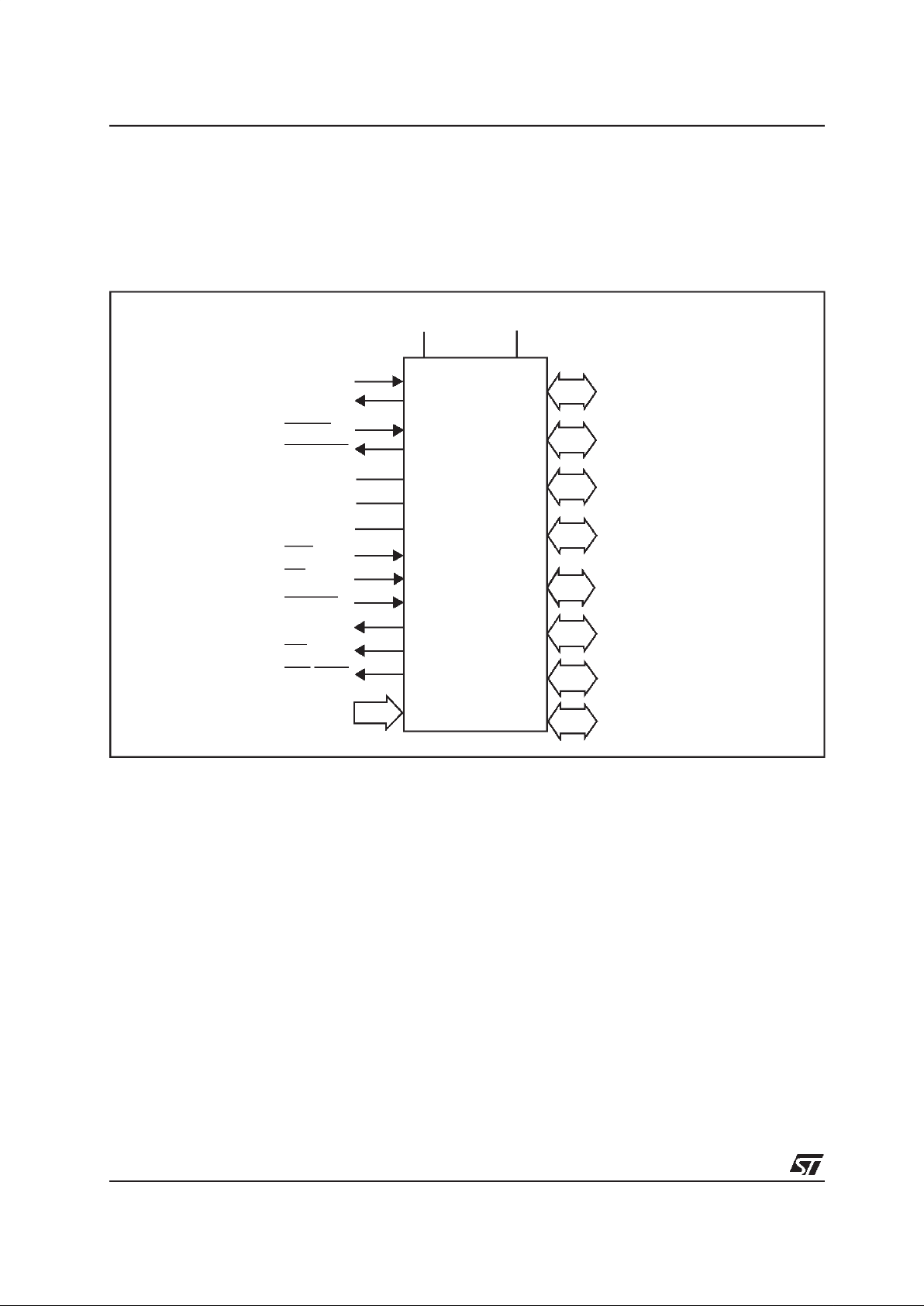
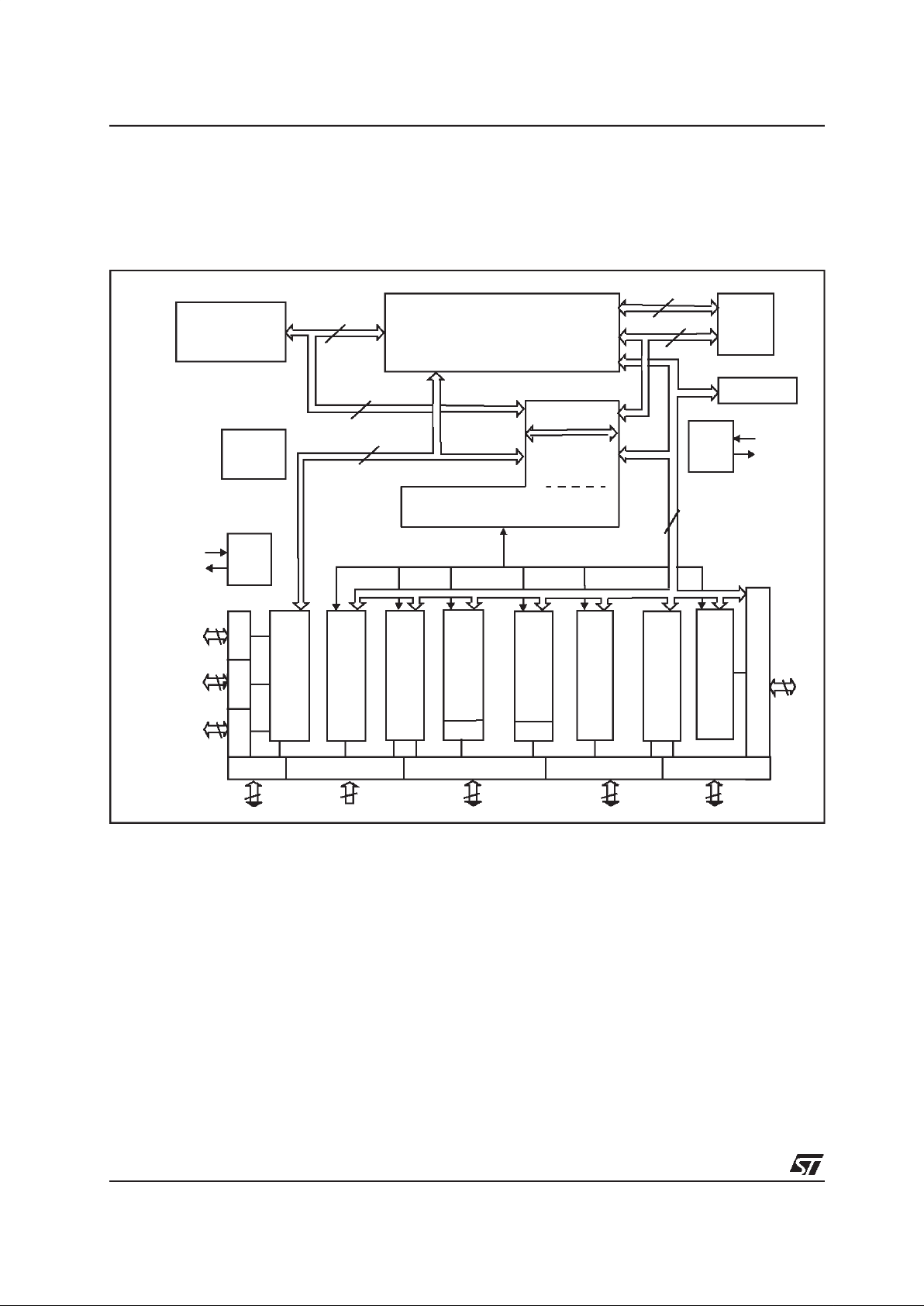
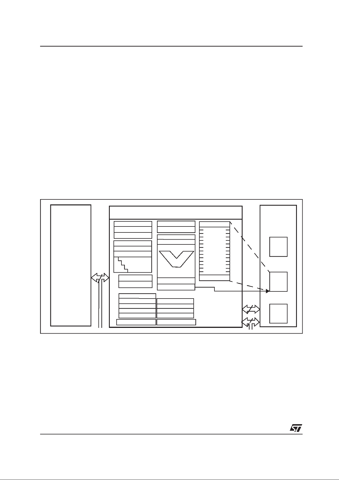
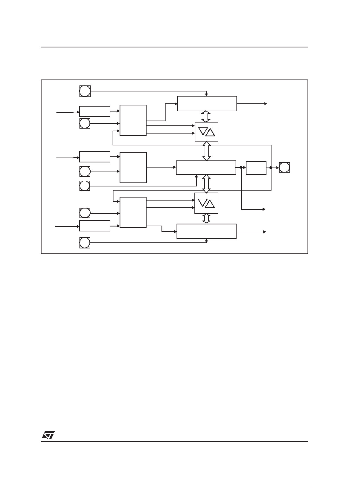
III - FUNCTIONAL DESCRIPTION
The architecture of the ST10C167 combines
advantages of both RISC and CISC processors
and an advanced peripheral subsystem. The
block diagram gives an overview of the different
on-chip componentsand thehigh bandwidth internal bus structureof the ST10C167.
Figure 3 : Block diagram
Port 0Port 1Port 4
Port 6
Port 5
Port 3
Port 2
GPT1
GPT2
ASC usart
BRG
CPU-Core
Internal
RAM
Watchdog
Interrupt Controller
32
16
PEC
16
16
CAN
Port 7
Port 8
External Bus
10-Bit ADC
BRG
SSC
PWM
CAPCOM2
CAPCOM1
OSC.
2K Byte
16
Controller
16
16
32K Byte ROM
for ST10C167
XRAM
XTAL1
XTAL2
CAN_RXD
CAN_TXD
8
16
16
16
8
15 8 8

ST10C167
11/65
IV - MEMORY ORGANIZATION
The memory space of the ST10C167 is
configured in a Von-Neumann architecture. Code
memory, data memory, registers and I/O ports are
organized within the samelinear address spaceof
16M Byte.
The entire memory space can be accessed Bytewise or Wordwise. Particular portions of the
on-chip memory have additionally been made
directly bit addressable.
ROM : 32KByte of on-chip ROM.
RAM : 2K Byte of on-chip internal RAM
(dual-port) is provided as a storage for data, system stack, general purpose register banks and
code. The register bank can consist of up to 16
wordwide (R0 to R15) and/or Bytewide (RL0,
RH0, …, RL7, RH7)general purpose registers.
XRAM : 2K Byte of on-chip extension RAM (single port XRAM) is provided as a storage for data,
user stack and code.
The XRAM isconnected to the internal XBUS and
is accessed like an external memory in 16-bit
demultiplexed bus-mode without waitstate or
read/write delay (80ns access at 25MHz CPU
clock). Byte and Word access is allowed.
The XRAM address range is 00’E000h 00’E7FFh if the XRAM is enabled (XPEN bit 2 of
SYSCON register). As the XRAM appears like
external memory, it cannot be used for the
ST10C167’s system stack or register banks. The
XRAM is not provided for single bit storage and
therefore is not bit addressable. If bit XRAMEN is
cleared, then any access in the address range
00’E000h - 00’E7FFh will be directed to external
memory interface, using the BUSCONx register
corresponding to address matching ADDRSELx
register.
SFR/ESFR : 1024 Byte (2 * 512 Byte) of address
space is reserved for the special function register
areas. SFRs are wordwide registers which are
used for controlling and monitoring functions of
the different on-chipunits.
CAN : Address range 00’EF00h - 00’EFFFh is
reserved forthe CAN Module access. TheCAN is
enabled by setting XPEN bit 2 of the SYSCON
register. Accesses to the CAN Module use demultiplexed addresses and a 16-bit data bus (Byte
accesses are possible). Two wait states give an
access time of 160ns at 25MHz CPU clock. No
tristate waitstate isused.
Note If the CAN module is used, Port 4 can not
be programmed to output all 8 segment
address lines. Thus, only 4 segment
address lines can be used, reducing the
external memory space to 5M Byte (1M
Byte per CS line).
In orderto meet the needs ofdesigns where more
memory is required than is provided on chip, up to
16M Byte of external RAM and/or ROM can be
connected to the microcontroller.
ST10C167
12/65
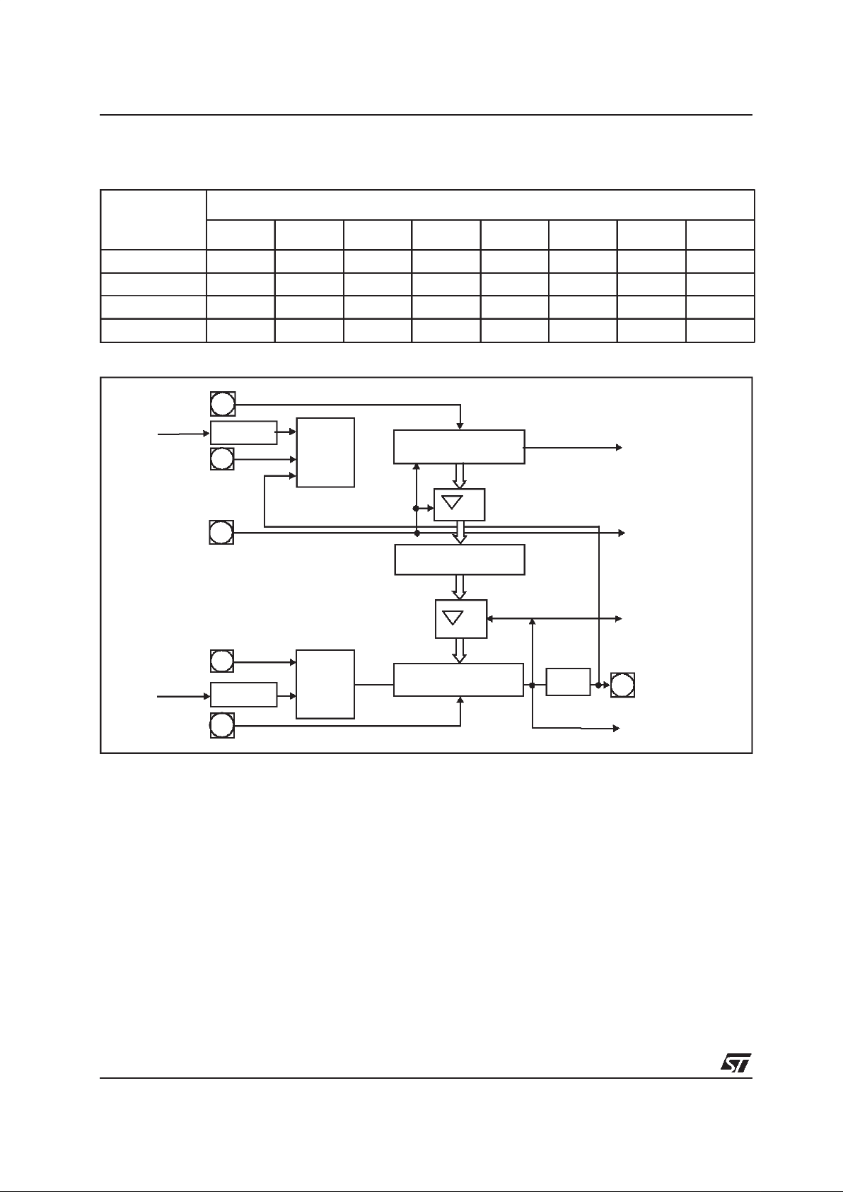
V - CENTRAL PROCESSING UNIT (CPU)
The CPUincludes a4-stage instruction pipeline, a
16-bit arithmetic and logic unit (ALU) and dedicated SFRs. Additionalhardware hasbeen added
for a separate multiply and divide unit, a bit-mask
generator and a barrel shifter.
Most of the ST10C167’s instructions can be executed in oneinstruction cycle which requires 80ns
at 25MHz CPU clock. For example, shift and
rotate instructions are processed in one instruction cycle independent of the number of bits to be
shifted. Multiple-cycle instructionshave been optimized: branches are carried out in 2 cycles, 16 x
16 bit multiplication in 5 cycles and a 32/16 bit
division in 10 cycles.The jump cache reduces the
execution time of repeatedly performed jumps in a
loop, from 2 cycles to 1 cycle.
The CPU uses an actual register context
consisting of up to16 Word wide GPRs physically
allocated within the on-chip RAM area. A Context
Pointer (CP) register determines the base
address ofthe active register bank to beaccessed
by the CPU. The number of register banks is only
restricted by the available internal RAM space.
For easy parameter passing, a register bank may
overlap others.
A systemstack of up to 1024 Byte is provided as a
storage for temporary data. The system stack is
allocated in the on-chip RAM area, and it is
accessed by the CPU via the stack pointer (SP)
register. Two separate SFRs, STKOV and
STKUN, are implicitly compared against the stack
pointer value upon each stack access for the
detection of a stack overflow orunderflow.
Figure 4 : CPU Block Diagram
32
Internal
RAM
2K Byte
General
Purpose
Registers
R0
R15
MDH
MLD
Barrel-Shift
Mul./Div.-HW
Bit-Mask Gen.
ALU
16-Bit
CP
SP
STKOV
STKUN
Exec. Unit
Instr. Ptr
Instr. Reg
4-Stage
Pipeline
PSW
SYSCON
BUSCON 0
BUSCON 1
BUSCON 2
BUSCON 3
BUSCON 4
ADDRSEL 1
ADDRSEL 2
ADDRSEL 3
ADDRSEL 4
Data Pg. Ptrs
Code Seg. Ptr.
CPU
32K Byte
on chip
ROM
16
16
Bank
n
Bank
i
Bank
0

ST10C167
13/65
VI - EXTERNAL BUS CONTROLLER
All of the external memory accesses are performed by the on-chip external bus controller. The
EBC can be programmed to single chip mode
when no external memory is required,or to one of
four different external memory access modes:
– 16-/18-/20-/24-bit addresses and 16-bit data,
demultiplexed.
– 16-/18-/20-/24-bit addresses and 16-bit data,
multiplexed.
– 16-/18-/20-/24-bit addresses and 8-bit data,
multiplexed.
– 16-/18-/20-/24-bit addresses and 8-bit data, de-
multiplexed.
In demultiplexed bus modes addresses are output
on Port1 and data is input/output on Port0 or P0L,
respectively. In the multiplexed bus modes both
addresses and data use Port0 for input/output.
Timing characteristics of the external bus interface (memory cycle time, memory tri-state time,
length of ALE and read/write delay) are programmable giving the choice of a wide range of memories and external peripherals. Up to 4 independent
address windows may be defined (using register
pairs ADDRSELx / BUSCONx) to access different
resources and bus characteristics. These address
windows are arranged hierarchically where
BUSCON4 overrides BUSCON3 and BUSCON2
overrides BUSCON1. All accesses to locations
not covered by these 4 address windows are controlled by BUSCON0. Up to 5 external CS signals
(4 windows plus default) can be generated in
order to save external glue logic. Access to very
slow memoriesis supportedby a ‘Ready’ function.
A HOLD/HLDA protocol is available for bus arbitration which shares external resources with other
bus masters. The bus arbitration is enabled by
setting bit HLDEN in register SYSCON. After setting HLDEN once, pins P6.7...P6.5 (BREQ,
HLDA, HOLD) are automatically controlled by the
EBC. In master mode (default after reset) the
HLDA pin is an output. By setting bit DP6.7 to’1’
the slave mode is selected where pin HLDA is
switched to input. This directly connects the slave
controller to another master controller without
glue logic.
For applications which require less external memory space, the address space can be restricted to
1M Byte, 256K Byte or to64K Byte.Port 4 outputs
all 8 address lines if an address space of
16M Byte is used, otherwise four, two or no
address lines.
Chip select timing can be made programmable.
By default (after reset), the CSx lines change half
a CPU clock cycle after the rising edge of ALE.
With the CSCFG bit set in the SYSCON register
the CSx lines change with the rising edge of ALE.
The active level of the READY pin can be set by
bit RDYPOLin the BUSCONx registers.When the
READY function is enabled for a specific address
window, each bus cycle within the window must
be terminated with the active level defined by bit
RDYPOL in theassociated BUSCON register.
ST10C167
14/65
VII - INTERRUPT SYSTEM
The interrupt response time for internal program
execution is from 200ns to 480ns.
The ST10C167 architecture supports several
mechanisms for fast and flexible response to service requests that can be generated from various
sources internal or external tothe microcontroller.
Any of these interrupt requests can be serviced by
the Interrupt Controller or by the Peripheral Event
Controller (PEC).
In contrast to a standard interrupt service where
the current program execution is suspended and
a branch to the interrupt vector table is performed,
just one cycle is ‘stolen’ from the current CPU
activity to perform a PEC service. A PEC service
implies a single Byte or Word data transfer
between any two memory locations with an additional increment of either the PEC source or the
destination pointer. An individual PEC transfer
counter is implicitly decremented for each PEC
service except when performing in the continuous
transfer mode. When this counter reaches zero, a
standard interrupt is performed to the corresponding source related vector location. PEC services
are very well suited, for example, for supporting
the transmission or reception of blocks of data.
The ST10C167 has 8 PEC channels each of
which offers such fast interrupt-driven data transfer capabilities.
A interrupt control register which contains an
interrupt request flag, an interrupt enable flag and
an interrupt priority bitfield is dedicated to each
existing interrupt source. Thanks to its related
register, each source can be programmed to one
of sixteen interrupt priority levels. Once starting to
be processed by the CPU, an interrupt service
can only be interrupted by a higher prioritized
service request. For the standard interrupt
processing, each of the possible interruptsources
has a dedicated vector location.
Fast external interrupt inputs are provided to service external interrupts with high precision
requirements. These fast interrupt inputs feature
programmable edge detection (rising edge, falling
edge or both edges).
Software interruptsare supportedbymeans of the
‘TRAP’ instruction in combination with an individual trap (interrupt)number.
Table 2 shows all the available ST10C167 interrupt sources and the corresponding hardware-related interrupt flags, vectors, vector
locations and trap (interrupt) numbers :
Table 2 : Interrupt sources
Source of Interrupt or PEC
Service Request
Request
Flag
Enable
Flag
Interrupt
Vector
Vector
Location
Trap
Number
CAPCOM Register 0 CC0IR CC0IE CC0INT 00’0040h 10h
CAPCOM Register 1 CC1IR CC1IE CC1INT 00’0044h 11h
CAPCOM Register 2 CC2IR CC2IE CC2INT 00’0048h 12h
CAPCOM Register 3 CC3IR CC3IE CC3INT 00’004Ch 13h
CAPCOM Register 4 CC4IR CC4IE CC4INT 00’0050h 14h
CAPCOM Register 5 CC5IR CC5IE CC5INT 00’0054h 15h
CAPCOM Register 6 CC6IR CC6IE CC6INT 00’0058h 16h
CAPCOM Register 7 CC7IR CC7IE CC7INT 00’005Ch 17h
CAPCOM Register 8 CC8IR CC8IE CC8INT 00’0060h 18h
CAPCOM Register 9 CC9IR CC9IE CC9INT 00’0064h 19h
CAPCOM Register 10 CC10IR CC10IE CC10INT 00’0068h 1Ah
CAPCOM Register 11 CC11IR CC11IE CC11INT 00’006Ch 1Bh
CAPCOM Register 12 CC12IR CC12IE CC12INT 00’0070h 1Ch
CAPCOM Register 13 CC13IR CC13IE CC13INT 00’0074h 1Dh
CAPCOM Register 14 CC14IR CC14IE CC14INT 00’0078h 1Eh
CAPCOM Register 15 CC15IR CC15IE CC15INT 00’007Ch 1Fh
CAPCOM Register 16 CC16IR CC16IE CC16INT 00’00C0h 30h
CAPCOM Register 17 CC17IR CC17IE CC17INT 00’00C4h 31h

ST10C167
15/65
CAPCOM Register 18 CC18IR CC18IE CC18INT 00’00C8h 32h
CAPCOM Register 19 CC19IR CC19IE CC19INT 00’00CCh 33h
CAPCOM Register 20 CC20IR CC20IE CC20INT 00’00D0h 34h
CAPCOM Register 21 CC21IR CC21IE CC21INT 00’00D4h 35h
CAPCOM Register 22 CC22IR CC22IE CC22INT 00’00D8h 36h
CAPCOM Register 23 CC23IR CC23IE CC23INT 00’00DCh 37h
CAPCOM Register 24 CC24IR CC24IE CC24INT 00’00E0h 38h
CAPCOM Register 25 CC25IR CC25IE CC25INT 00’00E4h 39h
CAPCOM Register 26 CC26IR CC26IE CC26INT 00’00E8h 3Ah
CAPCOM Register 27 CC27IR CC27IE CC27INT 00’00ECh 3Bh
CAPCOM Register 28 CC28IR CC28IE CC28INT 00’00E0h 3Ch
CAPCOM Register 29 CC29IR CC29IE CC29INT 00’0110h 44h
CAPCOM Register 30 CC30IR CC30IE CC30INT 00’0114h 45h
CAPCOM Register 31 CC31IR CC31IE CC31INT 00’0118h 46h
CAPCOM Timer 0 T0IR T0IE T0INT 00’0080h 20h
CAPCOM Timer 1 T1IR T1IE T1INT 00’0084h 21h
CAPCOM Timer 7 T7IR T7IE T7INT 00’00F4h 3Dh
CAPCOM Timer 8 T8IR T8IE T8INT 00’00F8h 3Eh
GPT1 Timer 2 T2IR T2IE T2INT 00’0088h 22h
GPT1 Timer 3 T3IR T3IE T3INT 00’008Ch 23h
GPT1 Timer 4 T4IR T4IE T4INT 00’0090h 24h
GPT2 Timer 5 T5IR T5IE T5INT 00’0094h 25h
GPT2 Timer 6 T6IR T6IE T6INT 00’0098h 26h
GPT2 CAPREL Register CRIR CRIE CRINT 00’009Ch 27h
A/D Conversion Complete ADCIR ADCIE ADCINT 00’00A0h 28h
A/D Overrun Error ADEIR ADEIE ADEINT 00’00A4h 29h
ASC0 Transmit S0TIR S0TIE S0TINT 00’00A8h 2Ah
ASC0 Transmit Buffer S0TBIR S0TBIE S0TBINT 00’011Ch 47h
ASC0 Receive S0RIR S0RIE S0RINT 00’00ACh 2Bh
ASC0 Error S0EIR S0EIE S0EINT 00’00B0h 2Ch
SSC Transmit SCTIR SCTIE SCTINT 00’00B4h 2Dh
SSC Receive SCRIR SCRIE SCRINT 00’00B8h 2Eh
SSC Error SCEIR SCEIE SCEINT 00’00BCh 2Fh
PWM Channel 0...3 PWMIR PWMIE PWMINT 00’00FCh 3Fh
CAN Interface XP0IR XP0IE XP0INT 00’0100h 40h
X-Peripheral Node XP1IR XP1IE XP1INT 00’0104h 41h
X-Peripheral Node XP2IR XP2IE XP2INT 00’0108h 42h
PLL Unlock XP3IR XP3IE XP3INT 00’010Ch 43h
Table 2 : Interrupt sources (continued)
Source of Interrupt or PEC
Service Request
Request
Flag
Enable
Flag
Interrupt
Vector
Vector
Location
Trap
Number
VII - INTERRUPT SYSTEM (continued)
ST10C167
16/65
Hardware traps are exceptions or error conditions
that arise during run-time. They cause immediate
non-maskable system reaction similar to a standard interrupt service (branching to a dedicated
vector table location).
The occurrence of a hardware trap is additionally
signified by an individual bit in the trap flag regis-
ter (TFR). Except when another higher prioritized
trap service is in progress, a hardware trap will
interrupt any actual program execution. In turn,
hardware trap services can normally not be interrupted by standard or PEC interrupts.
Table 3 shows all of the possible exceptions or
error conditions that can arise during run-time:
Table 3 : Exceptions or error conditions that can arise during run time
Exception Condition
Trap
Flag
Trap
Vector
Vector
Location
Trap
Number
Trap
Priority
Reset Functions:
Hardware Reset
Software Reset
Watchdog Timer Overflow
RESET
RESET
RESET
00’0000h
00’0000h
00’0000h
00h
00h
00h
III
III
III
Class A Hardware Traps:
Non-Maskable Interrupt
Stack Overflow
Stack Underflow
NMI
STKOF
STKUF
NMITRAP
STOTRAP
STUTRAP
00’0008h
00’0010h
00’0018h
02h
04h
06h
II
II
II
Class B Hardware Traps:
Undefined Opcode
Protected Instruction Fault
Illegal Word Operand
Access
Illegal Instruction Access
Illegal External Bus
Access
UNDOPC
PRTFLT
ILLOPA
ILLINA
ILLBUS
BTRAP
BTRAP
BTRAP
BTRAP
BTRAP
00’0028h
00’0028h
00’0028h
00’0028h
00’0028h
0Ah
0Ah
0Ah
0Ah
0Ah
I
I
I
I
I
Reserved [2Ch –3Ch] [0Bh – 0Fh]
Software Traps
TRAP Instruction
Any [00’0000h– 00’01FCh]
in steps of 4h
Any
[00h – 7Fh]
Current CPU
Priority
VII - INTERRUPT SYSTEM (continued)
ST10C167
17/65
VIII - CAPTURE/COMPARE (CAPCOM) UNIT
The ST10C167 has two 16 channel CAPCOM
units. They support generation and control of
timing sequences on up to 32 channels with a
maximum resolution of 320ns at 25MHz CPU
clock. The CAPCOM units are typically used to
handle high speed I/O tasks such as pulse and
waveform generation, pulse width modulation
(PMW), Digital to Analog (D/A) conversion,
software timing, or time recording relative to
external events.
Four 16-bit timers (T0/T1, T7/T8) with reload
registers provide two independent time bases for
the capture/compare register array.
The input clock for the timers is programmable to
several prescaled values of the internal system
clock, or may be derived from an overflow/
underflow of timer T6 in module GPT2. This
provides a wide range of variation for the timer
period and resolution and allows precise
adjustments to application specific requirements.
In addition, external count inputs for CAPCOM
timers T0 and T7 allow event scheduling for the
capture/compare registers relative to external
events.
Each of the two capture/compare register arrays
contain 16 dual purpose capture/compare
registers, each of which may be individually
allocated to either CAPCOM timer T0 or T1 (T7 or
T8, respectively), and programmed for capture or
compare functions. Each register has one
associated port pin which serves as an input pin
for triggering the capture function, or as an output
pin (except for CC24...CC27) to indicate the
occurrence of acompare event.
When a capture/compare register has been
selected forcapture mode, thecurrent contents of
the allocated timer will be latched (captured) into
the capture/compare register in response to an
external event at the port pin which is associated
with this register. In addition, a specific interrupt
request for this capture/compare register is
generated. Either a positive, a negative, or both a
positive and a negative external signal transition
at the pin can be selected as the triggering event.
The contents of all registers which have been
selected for one of the five compare modes are
continuously compared with the contents of the
allocated timers. When a match occurs between
the timer value and the value in a capture/
compare register, specific actions will be taken
based on the selected compare mode (see
Table 4).
The input frequencies fTxforTx aredetermined as
a function of the CPU clocks. The formulas are
detailed in the user manual. The timer input frequencies, resolution and periods which result
from the selected pre-scaler option in TxI when
using a 25MHz CPU clock are listed in the table
below. The numbers for the timer periods are
based ona reload value of0000H. Note that some
numbers may be rounded to 3 significant figures
(see Table5).
Table 4 : Compare modes
Compare Modes Function
Mode 0 Interrupt-only compare mode ; several compare interrupts per timer period are possible
Mode 1 Pin toggles on each compare match ; several compare events per timer period are possible
Mode 2 Interrupt-only compare mode ; only one compare interrupt per timer period is generated
Mode 3 Pin set ‘1’ on match; pin reset ‘0’ on compare time overflow ; only one compare event per
timer period is generated
Double Register Mode Two registers operate on one pin; pin toggles on each compare match ; several compare
events per timer period are possible.
Table 5 : CAPCOM timer input frequencies, resolution and periods
f
CPU
= 25MHz
Timer Input Selection TxI
000
B
001
B
010
B
011
B
100
B
101
B
110
B
111
B
Pre-scaler for f
CPU
8 16 32 64 128 256 512 1024
Input Frequency 3.125MHz 1.56MHz 781KHz 391KHz 195KHz 97.7KHz 48.8KHz 24.4KHz
Resolution 320ns 640ns 1.28µs 2.56µs 5.12µs 10.24µs 20.48µs 40.96µs
Period 21.0ms 41.9ms 83.9ms 167ms 336ms 671ms 1.34s 2.68s

ST10C167
18/65
IX - GENERAL PURPOSE TIMER UNIT
The GPT unit is a flexible multifunctional timer/
counter structure which is used for time related
tasks such as event timing and counting, pulse
width and duty cycle measurements, pulse
generation, or pulse multiplication. The GPT unit
contains five 16-bit timers organized into two
separate modules GPT1and GPT2.Each timer in
each module may operate independently in
several different modes, or may be concatenated
with another timer of the same module.
IX.1 - GPT1
Each of the three timers T2, T3, T4 of the GPT1
module can be configured individually for one of
four basic modes of operation: timer, gated
timer, counter mode and incremental interface
mode. In timer mode, the inputclock for a timer is
derived from the CPU clock, divided by a programmable prescaler. In counter mode, the timer
is clocked in reference to external events. Pulse
width or duty cycle measurement is supported in
gated timermode where theoperation ofa timer is
controlled by the ‘gate’ level on an external input
pin. For these purposes, each timer has oneassociated port pin (TxIN) which is the gate or the
clock input.
The table below lists the timer input frequencies,
resolution and periods for each pre-scaler option
at 25MHz CPU clock. This also applies to the
Gated Timer Mode of T3 and to the auxiliary
timers T2 and T4 inTimer and Gated Timer Mode
(see Table6).
The count direction (up/down) for each timer is
programmable by software or may additionally be
altered dynamically by an external signal ona port
pin (TxEUD).
In Incremental Interface Mode, the GPT1 timers
(T2, T3, T4) can be directly connected to the
incremental position sensor signals A and B by
their respective inputs TxIN and TxEUD. Direction
and count signals are internally derived from
these two input signals so that the contentsof the
respective timer Tx corresponds to the sensor
position. The third position sensor signal TOP0
can be connected to an interrupt input.
TimerT3 hasoutput toggle latches (TxOTL)which
changes state on each timer over-flow/underflow.
The state of this latch may be output on port pins
(TxOUT) e. g. for time out monitoring of external
hardware components, or may be used internally
to clock timers T2 and T4 for high resolution measurement of long timeperiods.
In addition to their basic operating modes, timers
T2 andT4 maybe configured as reload or capture
registers for timer T3. When used as capture or
reload registers, timers T2 and T4 are stopped.
The contents of timer T3 is captured into T2 or T4
in response to a signal at their associated input
pins (TxIN). Timer T3 is reloaded with the
contents of T2 or T4 triggered either by an
external signal or by a selectable state transition
of its toggle latch T3OTL. When both T2 and T4
are configured to alternately reload T3 on
opposite state transitions of T3OTL with the low
and high times of a PWM signal, this signal
can be constantly generated without software
intervention.
Table 6 : GPT1 timer input frequencies, resolution and periods
f
CPU
= 25MHz
Timer Input Selection T2I / T3I / T4I
000
B
001
B
010
B
011
B
100
B
101
B
110
B
111
B
Pre-scaler factor 8 16 32 64 128 256 512 1024
Input Frequency 3.125MHz 1.563MHz 781.3KHz 390.6KHz 195.3KHz 97.66KHz 48.83KHz 24.41KHz
Resolution 320ns 640ns 1.28µs 2.56µs5.12µs 10.24µs 20.48µs 40.96µs
Period 21.0ms 41.9ms 83.9ms 167ms 336ms 671ms 1.34s 2.68s
ST10C167
19/65
IX.2 - GPT2
The GPT2 module provides precise event control
and timemeasurement. Itincludes two timers (T5,
T6) and a capture/reload register (CAPREL). Both
timers can be clocked with an input clock which is
derived from the CPU clock via a programmable
prescaler or with external signals. The count
direction (up/down) for each timer is programmable by software or may additionally be altered
dynamically by an external signal on a port pin
(TxEUD). Concatenation of the timers is supported via the output toggle latch (T6OTL) of timer
T6 which changes its state on each timer overflow/underflow.
The state of this latch may be used to clock timer
T5, orit may be output on a port pin (T6OUT). The
overflows/underflows of timer T6 can additionally
be used to clock the CAPCOM timers T0 or T1,
and to cause a reload from the CAPREL register.
The CAPREL register may capture the contentsof
timer T5 based on an external signal transition on
the corresponding port pin (CAPIN), and timer T5
may optionallybe cleared after the capture procedure. This allows absolute time differences to be
measured or pulse multiplication to be performed
without software overhead.
The capture trigger (timer T5 to CAPREL) may
also be generated upon transitions of GPT1 timer
T3 inputs T3IN and/or T3EUD. This is advantageous when T3 operates in Incremental Interface
Mode.
Table 7 lists thetimer input frequencies, resolution
and periods for each pre-scaler option at 25MHz
CPU clock.
This also applies to the Gated Timer Mode of T6
and to the auxiliary timer T5 in Timer and Gated
Timer Mode.
Figure 5 : Block diagram of GPT1
2nn=3...10
2nn=3...10
2nn=3...10
T2EUD
T2IN
CPU Clock
CPU Clock
CPU Clock
T3EUD
T4IN
T3IN
T4EUD
T2
Mode
Control
T3
Mode
Control
T4
Mode
Control
GPT1 Timer T2
GPT1 Timer T3
GPT1 Timer T4
T3OTL
Reload
Capture
U/D
U/D
Reload
Capture
Interrupt
Request
Interrupt
Request
Interrupt
Request
T3OUT
U/D
IX - GENERAL PURPOSE TIMER UNIT (continued)
ST10C167
20/65
Table 7 : GPT2 timer input frequencies, resolution and periods
f
CPU
= 25MHz
Timer Input Selection T5I /T6I
000B 001B 010B 011B 100B 101B 110B 111B
Pre-scaler factor 4 8 16 32 64 128 256 512
Input Frequency 6.25MHz 3.125MHz 1.563MHz 781.3KHz 390.6KHz 195.3KHz 97.66KHz 48.83KHz
Resolution 160ns 320ns 640ns 1.28µs 2.56µs 5.12µs 10.24µs 20.48µs
Period 10.49ms 21.0ms 41.9ms 83.9ms 167ms 336ms 671ms 1.34s
Figure 6 : Block diagram of GPT2
2nn=2...9
2nn=2...9
T5EUD
T5IN
CPU Clock
CPU Clock
T6IN
T6EUD
T5
Mode
Control
T6
Mode
Control
GPT2 Timer T5
GPT2 Timer T6
U/D
Interrupt
Request
U/D
GPT2 CAPREL
T60TL
Toggle FF
T6OUT
CAPIN
Reload
Interrupt
Request
to CAPCOM
Timers
Capture
Clear
Interrupt
Request
IX - GENERAL PURPOSE TIMER UNIT (continued)

ST10C167
21/65
X - PWM MODULE
The pulse width modulation module can generate
up to four PWM output signals using edge-aligned
or centre-aligned PWM. In addition, the PWM
module can generate PWM burst signals and sin-
gle shot outputs. Table 8 shows the PWM frequencies for different resolutions. The level of the
output signals is selectable and the PWM module
can generate interruptrequests.
Table 8 : PWM unit frequencies and resolution at 25MHz clock
Mode 0 Resolution 8-bit 10-bit 12-bit 14-bit 16-bit
CPU Clock/1 40ns 97.66KHz 24.41KHz 6.104KHz 1.526KHz 0.381KHz
CPU Clock/64 2.56ns 1.526KHz 381.5Hz 95.37Hz 23.84Hz 5.96Hz
Mode 1 Resolution 8-bit 10-bit 12-bit 14-bit 16-bit
CPU Clock/1 40ns 48.82KHz 12.20KHz 3.05KHz 762.9Hz 190.7Hz
CPU Clock/64 2.56ns 762.9Hz 190.7 Hz 47.68Hz 11.92Hz 2.98Hz
Figure 7 : Block diagram of PWM module
PPxPeriodRegister
Comparator
PTx
16-BitUp/DownCounter
ShadowRegister
PWxPulseWidthRegister
Input
Run
Control
Clock1
Clock2
Comparator
*
*
*
Up/Down/
ClearControl
Match
OutputControl
Match
Write Control
*
Userread-&writeable
Enable
POUTx

ST10C167
22/65
XI - PARALLEL PORTS
The ST10C167 provides up to 111 I/O lines organized into eight input/output ports and one input
port.
All port lines are bit-addressable, and all input/output lines are individually (bit-wise) programmable
as input or output via direction registers. The I/O
ports are true bidirectional ports which are
switched to high impedance state when configured as inputs.
The output drivers of five I/O ports can be configured (pin by pin) for push/pull operation or
open-drain operation via control registers. During
the internal reset, all port pins are configured as
inputs.
The input threshold of Port 2, Port 3, Port 7 and
Port 8 is selectable (TTL-or CMOS-like), where
the special CMOS-like input threshold reduces
noise sensitivity due to the input hysteresis.
The input thresholds are selected with bit of
PICON register dedicated to blocksof 8 input pins
(2-bit for port2, 2-bit for port3, 1-bit for port7, 1-bit
for port8).
All pins of I/O ports also support an alternate programmable function:
– Port0 and Port1 may be used as address and
data lines when accessing external memory.
– Port 2, Port 7 and Port 8are associatedwith the
capture inputs or with the compare outputs of
the CAPCOM units and/or with the outputs of
the PWM module.
– Port 3 includes the alternate functions of timers,
serial interfaces, the optional bus control signal
BHE and thesystem clock output (CLKOUT).
– Port 4 outputs the additional segment address
bits A16 to A23 insystems where segmentation
is enabled to access more than 64K Byte of
memory.
– Port 5 is used as analog input channels of the
A/Dconverter or as timer control signals.
– Port 6 provides optional bus arbitration signals
(BREQ, HLDA,HOLD) and chip select signals.
All port lines that are not used for alternate functions may be used as general purpose I/O lines.

ST10C167
23/65
XII - A/D CONVERTER
A10-bit A/D converter with 16 multiplexed input
channels and a sample and hold circuit is integrated on-chip. The sample time (for loading the
capacitors) and the conversion time is programmable and can be adjusted tothe external circuitry.
Overrun error detection/protection is controlled by
the ADDAT register. Either an interrupt request is
generated when the result of a previous conversion has not been read from the result register at
the time the next conversion is complete, or the
next conversion is suspended until the previous
result has been read. For applications which
require less than 16 analog input channels, the
remaining channel inputs can be used as digital
input port pins. The AD converter of the
ST10F168 supports different conversion modes :
– Single channel single conversion:the analog
level of the selected channel is sampled once
and converted. The result of the conversion is
stored in the ADDAT register.
– Single channel continuous conversion : the
analog levelof the selected channel is repeatedly
sampled and converted.The result ofthe conversion is stored in the ADDAT register.
– Auto scansingle conversion : theanalog level
of the selected channels are sampled once and
converted. After each conversion the result is
stored in the ADDAT register. The data can be
transfered to the RAM by interrupt software
management or using the powerfull Peripheral
Event Controller data transfert.
– Auto scan continuous conversion : the ana-
log levelofthe selected channels arerepeatedly
sampled and converted. The result of the conversion is stored in the ADDAT register. The
data can be transfered to the RAM by interrupt
software management or using the powerfull
Peripheral Event Controller data transfert.
– Wait for ADDAT read mode : when using con-
tinuous modes, in order to avoid to overwrite
the result of the current conversion by the next
one, the ADWR bit of ADCON control register
must be activated. Then,until the ADDAT register is read, the new result is stored in a temporary buffer and the conversion is on hold.
– Channel injection mode : when using
continuous modes, a selected channel can be
converted in between without changing the
current operating mode. The 10 bit data of the
conversion are stored in ADRES field of
ADDAT2.The current continuous moderemains
active after the single conversion is completed.
The Table : 9 ADC sample clock and conversion
time shows the ADC unit conversion clock,sample
clock.
A complete conversion will take 14tCC+2tSC+
4 TCL. This time includes the conversion it-self,
the sampling time and the time required to transfer the digital value to the result register. For
example, at 25MHz of CPU clock, minimum complete conversion time is 7.76µs.
The A/D converter provides automatic offset and
linearity self calibration. The calibration operation
is performed in two ways:
– A full calibration sequence is performed after a
reset and lasts 1.6ms minimum (at 25MHz CPU
clock). During this time, the ADBSY flag is set to
indicate the operation. Normal conversion can
be performed during this time. The duration of
the calibration sequence isthenextended by the
time consumed by the conversions.
Note : After a power-on reset, the total
unadjusted error (TUE) of the ADC might be
worse than ±2LSB (max.±4LSB). During the full
calibration sequence, the TUE is constantly
improved until at the end of the cycle, TUE is
within the specified limits of ±2LSB.
– One calibration cycle is performed after each
conversion : each calibration cycle takes 4 ADC
clock cycles. These operation cycles ensure
constant updating of the ADC accuracy, compensating changing operating conditions.
Note 1. See chapter XX.
2. t
CC
= TCL x 24.
Table 9 : ADC sample clock and conversion time
ADCTC
Conversion Clock t
CC
ADSTC
Sample Clock t
SC
TCL1= 1/2 x f
XTAL
At f
CPU
= 25MHz
-
At f
CPU
= 25MHz
00 TCL x 24 0.48µs00 t
CC 0.48µs
2
01 Reserved, do not use - 01 tCCx2
0.96µs
2
10 TCL x 96 1.92µs10t
CC
x4
1.92µs
2
11 TCL x 48 0.96µs11t
CC
x8
3.84µs
2

ST10C167
24/65
XIII - SERIAL CHANNELS
Serial communication with other microcontrollers,
processors, terminals or external peripheral components is provided by two serial interfaces: the
asynchronous/synchronous serial channel
(ASC0) and the high-speed synchronous serial
channel (SSC).
Two dedicated Baud rate generators set up all
standard Baud rates without the requirement of
oscillator tuning.
For transmission, reception and erroneous reception, 3 separate interrupt vectors are provided for
each serial channel.
ASCO
ASCO supports full-duplex asynchronous
communication up to 781.25K Baud and
half-duplex synchronous communication up to
5M Baud at 25MHz system clock. For
asynchronous operation, the Baud rate generator
provides a clock with 16 times the rate of the
established Baud rate.
The table below lists various commonly used
Baud rates together with the required reload values and the deviation errors compared to the
intended Baud rate (see Table 10).
For synchronous operation, the Baudrate generator provides a clock with 4 times the rate of the
established Baud rate.
Note The deviation errors given in the table above are rounded. Using a Baud rate crystal will provide correct Baud rates without deviation
errors.
Table 10 : Commonly used Baud rates by reload value and deviation errors
S0BRS = ‘0’, f
CPU
= 25MHz S0BRS = ‘1’, f
CPU
= 25MHz
Baud Rate (Baud) Deviation Error Reload Value Baud Rate (Baud) Deviation Error Reload Value
781250 ±0.0% 0000
H
520833 ±0.0% 0000
H
56000 +7.3% / -0.4% 000CH/ 000D
H
56000 +3.3% / -7.0% 0008H / 0009H
38400 +1.7% / -3.1% 0013
H
/ 0014
H
38400 +4.3% / -3.1% 000CH / 000DH
19200 +1.7% / -0.8% 0027
H
/ 0028
H
19200 +0.5% / -3.1% 001AH / 001BH
9600 +0.5% / -0.8% 0050
H
/ 0051
H
9600 +0.5% / -1.4% 0035H / 0036H
4800 +0.5% / -0.1% 00A1
H
/ 00A2
H
4800 +0.5% / -0.5% 006BH / 006CH
2400 +0.2% / -0.1% 0144
H
/ 0145
H
2400 +0.0% / -0.5% 00D8H / 00D9H
1200 +0.0% / -0.1% 028A
H
/ 028B
H
1200 +0.0% / -0.2% 01B1H /01B2H
600 +0.0% / -0.1% 0515
H
/ 0516
H
600 +0.0% / -0.1% 0363H / 0364H
95 +0.4% / 0.4% 1FFF
H
/ 1FFF
H
75 +0.0% / 0.0% 1B1FH / 1B20H
63 +0.9% / 0.9% 1FFFH / 1FFFH

ST10C167
25/65
High Speed Synchronous SerialChannel(SSC)
The High-Speed Synchronous Serial Interface
SSC provides flexible high-speed serial
communication between theST10C167 and other
microcontrollers, microprocessors or external
peripherals.
The SSC supports full-duplex and half-duplex
synchronous communication; The serial clock
signal can begenerated by the SSC itself (master
mode) or be received from an external master
(slave mode). Data width, shift direction, clock
polarity and phase are programmable. This allows
communication with SPI-compatible devices.
Transmission and reception of data is
double-buffered. A 16-bit Baud rate generator
provides the SSC with a separate serial clock
signal. The serial channel SSC has its own
dedicated 16-bit Baud rate generator with 16-bit
reload capability, allowing Baud rate generation
independent from thetimers.
SSCBR isthe dual-function Baud Rate Generator/
Reload register. Table11 lists some possible
Baud ratesagainst the required reload values and
the resulting bit times for a 25MHz CPU clock.
Table 11 : Synchronous Baud rate andreload values
Baud Rate Bit Time Reload Value
Reserved use a reload value > 0. --- 0000
H
5M Baud 200ns 0001
H
3.3M Baud 303ns 0002
H
2.5M Baud 400ns 0004
H
2M Baud 500ns 0005
H
1M Baud 1µs 000B
H
100K Baud 10µs 007C
H
10K Baud 100µs 04E1
H
1K Baud 1ms 30D3
H
190.7 Baud 5.2ms FFFF
H
XIII - SERIAL CHANNELS (continued)

ST10C167
26/65
XIV - CAN MODULE
The integrated CAN module handles the completely autonomous transmission and reception of
CAN frames in accordance with the CAN specification V2.0 part B (active) i.e. the on-chip CAN
module can receive and transmit standard frames
with 11-bit identifiers as well as extended frames
with 29-bit identifiers.
The CAN module provides full CAN functionality
on up to 15 message objects. Message object 15
can be configured for basic CAN functionality.
Both modes provide separate masks for acceptance filtering, allowing a number of identifiers in
full CAN mode to be accepted and disregarding a
number of identifiers in basic CAN mode.
All message objects can be updated independent
from other objects and are equipped for the maximum message length of 8 Byte.
The bittiming is derivedfrom theXCLK and is programmable up to a data rate of 1M Baud. The
CAN module uses two pins to interface to a bus
transceiver.
XV - WATCHDOG TIMER
The Watchdog Timer is a fail-safe mechanism
which prevents the microcontroller from malfunctioning for long periods of time. The Watchdog
Timer is always enabled after a reset of the chip
and can only be disabled in the time interval until
the EINIT (end of initialization) instruction has
been executed. Therefore, the chip start-up procedure is always monitored. The software must
be designed to service the watchdog timer before
it overflows. If, due to hardware or software
related failures, the software fails to do so, the
watchdog timer overflows and generates an internal hardwarereset. Itpulls theRSTOUT pin low in
order to allow external hardware components to
be reset.
The Watchdog Timer is 16-bit, clocked with the
system clockdivided by2 or 128. The high Byte of
the watchdog timer register can be set to a
pre-specified reload value (stored in WDTREL).
Each time it is serviced by the application software, the high Byte of the watchdog timer is
reloaded.
For security, rewrite WDTCON each
time before the watchdog timer is serviced
Table 12 : Watchdog time range for 25MHz CPU clock
Reload value in WDTREL
Prescaler for f
CPU
2 (WDTIN = ‘0’) 128 (WDTIN = ‘1’)
FF
H
20.48µs 1.31ms
00
H
5.24ms 336ms

ST10C167
27/65
XVI - INSTRUCTION SET SUMMARY
The table below lists the instructions of the
ST10C167. The various addressing modes,
instruction operation, parameters for conditional
execution of instructions, opcodes and a detailed
description ofeach instruction can be found in the
“ST10 Family Programming Manual”.
Table 13 : Instruction set summary
Mnemonic Description Bytes
ADD(B) Add Word (Byte) operands 2 / 4
ADDC(B) Add Word (Byte) operands with Carry 2 / 4
SUB(B) Subtract Word (Byte) operands 2 / 4
SUBC(B) Subtract Word (Byte) operands with Carry 2 / 4
MUL(U) (Un)Signed multiply direct GPR by direct GPR (16-16-bit) 2
DIV(U) (Un)Signed divide register MDL by direct GPR (16-/16-bit) 2
DIVL(U) (Un)Signed long divide register MD by direct GPR (32-/16-bit) 2
CPL(B) Complement direct Word (Byte) GPR 2
NEG(B) Negate direct Word (Byte) GPR 2
AND(B) Bitwise AND, (Word/Byte operands) 2 / 4
OR(B) Bitwise OR, (Word/Byte operands) 2 / 4
XOR(B) Bitwise XOR, (Word/Byte operands) 2 / 4
BCLR Clear direct bit 2
BSET Set direct bit 2
BMOV(N) Move (negated) direct bit to direct bit 4
BAND, BOR, BXOR AND/OR/XOR direct bit with direct bit 4
BCMP Compare direct bit to direct bit 4
BFLDH/L Bitwise modify masked high/low byte of bit-addressable
direct Word memory with immediate data
4
CMP(B) Compare Word (Byte) operands 2 / 4
CMPD1/2 Compare Word data to GPR and decrement GPR by 1/2 2 / 4
CMPI1/2 Compare Word data to GPR and increment GPR by 1/2 2 / 4
PRIOR Determine number of shift cycles to normalize direct Word GPR and store
result in direct Word GPR
2
SHL / SHR Shift left/right direct WordGPR 2
ROL / ROR Rotate left/right direct Word GPR 2
ASHR Arithmetic (sign bit) shift right direct Word GPR 2
MOV(B) Move Word (Byte) data 2 / 4
MOVBS Move Byte operand to Word operand with sign extension 2 / 4
MOVBZ Move Byte operand to Word operand. with zero extension 2 / 4
JMPA, JMPI, JMPR Jump absolute/indirect/relative if condition is met 4
JMPS Jump absolute to a code segment 4
J(N)B Jump relative if direct bit is (not) set 4
JBC Jump relative and clear bit if direct bit is set 4

ST10C167
28/65
JNBS Jump relative and setbit if direct bit is not set 4
CALLA, CALLI, CALLR Call absolute/indirect/relative subroutine if condition is met 4
CALLS Call absolute subroutine in any code segment 4
PCALL Push direct Word register onto system stack & call absolute subroutine 4
TRAP Call interrupt service routine via immediate trap number 2
PUSH, POP Push/pop direct Word register onto/from system stack 2
SCXT Push direct Word register onto system stack and update register with Word
operand
4
RET Return from intra-segment subroutine 2
RETS Return from inter-segment subroutine 2
RETP Return from intra-segment subroutine and pop direct Word register from
system stack
2
RETI Return from interrupt service subroutine 2
SRST Software Reset 4
IDLE Enter Idle Mode 4
PWRDN Enter Power Down Mode (assumes NMI-pin low) 4
SRVWDT Service Watchdog Timer 4
DISWDT Disable Watchdog Timer 4
EINIT Signify End-of-Initialization on RSTOUT-pin 4
ATOMIC Begin ATOMIC sequence 2
EXTR Begin EXTended Register sequence 2
EXTP(R) Begin EXTendedPage (and Register) sequence 2 / 4
EXTS(R) Begin EXTendedSegment (and Register) sequence 2 / 4
NOP Null operation 2
Table 13 : Instruction set summary (continued)
Mnemonic Description Bytes
XVI - INSTRUCTION SET SUMMARY (continued)

ST10C167
29/65
XVII - SYSTEM RESET
The internal system reset function is invoked
either by asserting a hardware reset signal on pin
RSTIN (Hardware Reset Input), by the execution
of the SRST instruction (Software Reset) or by an
overflow of the watchdog timer. Whenever one of
these conditions occurs, the microcontroller is
reset into its predefined default state. The
following type of reset are implemented on the
ST10C167:
Asynchronous hardware reset
Asynchronous reset does not require a stabilized
clock signal onXTAL1, asit isnot internally resynchronized. It immediately resets the microcontroller into its default reset state.
This asynchronous reset is required upon
power-up of the chip and maybe used during catastrophic situations. The rising edge of the RSTIN
pin is internally resynchronized before exiting the
reset condition. Therefore, only the entry of this
hardware reset is asynchronous.
Synchronous hardware reset (warm reset)
A warm synchronous hardware reset is triggered
when the reset input signal RSTIN is latched low
and RPD (Pin 84) is high. The I/Os are
immediately (asynchronously) set in high
impedance, RSTOUT is driven low. After negation
of RSTIN is detected, a short transition period
elapses, during which pending internal hold states
are cancelled and any current internal access
cycles are completed, external bus cycles are
aborted.
Then, the internal reset sequence starts for 1024
TCL (512 CPU clock cycles). During this reset
sequence, if bit BDRSTEN was previously set by
software (bit 5 in SYSCON register), RSTIN pin is
driven low and internal reset signal is asserted to
reset the microcontroller in its default state. Note
that after all reset sequences, bit BDRSTEN is
cleared.
After the reset sequence hasbeen completed,the
RSTIN input is sampled. If the reset input signal is
active at that time the internal reset condition is
prolonged until RSTIN becomes inactive.
Software reset
The reset sequence can be triggered at any time
by the protected instruction SRST (software
reset). This instruction can be executed
deliberately within a program, e.g. to leave
bootstrap loader mode, or on a hardwaretrap that
reveals a system failure. As for a synchronous
hardware reset, the reset sequence lasts 1024
TCL (512 CPU clock cycles), and drives the
RSTIN pin low.
Watchdog timer reset
When the watchdog timer is not disabled during
the initialization or serviced regularly during
program execution it will overflow and trigger the
reset sequence.
Unlike hardware and software resets, the watchdog reset completes a running external bus cycle
if this bus cycle either does not use READY, or if
READY is sampled active (low) after the programmed waitstates.
When READY is sampled inactive (high) after the
programmed waitstates the running external bus
cycle is aborted. The internal reset sequence is
then started. The watchdog reset cannot occur
while the ST10C167 is in bootstrap loader mode.
Bidirectional reset
This feature is enabled by bit 3 of the SYSCON
register. The bidirectional reset makes the watchdog timer reset and software reset externally visible. It is active for the duration of an internal reset
sequences causedby a watchdog timer reset and
software reset.
This means that the bidirectional reset transforms
an internal watchdog timer reset or software reset
into an external hardware reset with a minimum
duration of 1024 TCL. The consequence is that
during a watchdog timer reset or software reset,
the behavior of the ST10C167 is equal to an
external hardware reset.

ST10C167
30/65
XVIII - POWER REDUCTION MODES
Two different power reduction modes with different levels of power reduction can be entered
under software control.
In Idle mode the CPU is stopped, while the
peripherals continue their operation. Idle mode
can be terminated by any reset or interrupt
request.
In Power Down mode both the CPU and the
peripherals are stopped. Power Down mode can
be configured by software in order to be terminated only by a hardware reset or by an external
interrupt source on fast external interrupt pins.
There are two different operating Power Down
modes:
– Protected power down mode: selected byset-
ting bit PWDCFGin the SYSCON register to ‘0’.
This mode can be used in conjunction with an
external power failuresignal which pulls theNMI
pin low when a power failure is imminent. The
microcontroller enters the NMI trap routine and
saves the internal state into RAM. Thetrap routine then sets a flag or writes a bit pattern into
specific RAM locations, and executes the
PWRDN instruction. If the NMI pin is still low at
this time, Power Down mode will be entered, if
not program execution continues. During power
downthe voltage at the VCCpins can belowered
to2.5 V and the contents oftheinternal RAM will
still be preserved.
– Interruptible power down mode: this
mode is selected by setting bit PWDCFG in the
SYSCON register. The CPU and peripheral
clocks are frozen, and the oscillator andPLL are
stopped. To exit power down mode with an external interrupt, an EXxIN (x = 7...0) pin has to
be asserted for at least 40ns. This signal enables the internal oscillator and PLL circuitry, and
turns on theweak pull-down.If theInterrupt was
enabled before entering power down mode, the
device executes the interrupt service routine,
and then resumes execution after the PWRDN
instruction. If the interrupt was disabled, the device executes the instruction following PWRDN
instruction, and the Interrupt Request Flag remains set until it is cleared by software.
All external bus actions are completed before Idle
or Power Down mode isentered. However, Idle or
Power Down mode is not entered if READY is
enabled, but has not been activated during the
last bus access.

ST10C167
31/65
XIX - SPECIAL FUNCTION REGISTER OVERVIEW
Table 14 lists all SFRs which are implemented
in the ST10C167 in alphabetical order.
Bit-addressable SFRs are marked with the letter
“b” in column “Name”. SFRs within the Extended
SFR-Space (ESFRs) are marked with the letter
“E” in column “Physical Address”.
An SFR can be specified by its individual
mnemonic name. Depending on the selected
addressing mode,an SFR can beaccessed via its
physical address (using the Data Page Pointers),
or via its short 8-bit address (without using the
Data Page Pointers).
Table 14 : Special function registers listed by name
Name
Physical
address
8-bit
address
Description
Reset
value
ADCIC b FF98h CCh A/D Converter End Of Conversion Interrupt Control Register 0000h
ADCON b FFA0h D0h A/D Converter Control Register 0000h
ADDAT FEA0h 50h A/D Converter Result Register 0000h
ADDAT2 F0A0h E 50h A/D Converter 2 Result Register 0000h
ADDRSEL1 FE18h 0Ch Address Select Register 1 0000h
ADDRSEL2 FE1Ah 0Dh Address Select Register 2 0000h
ADDRSEL3 FE1Ch 0Eh Address Select Register 3 0000h
ADDRSEL4 FE1Eh 0Fh Address Select Register 4 0000h
ADEIC b FF9Ah CDh A/D Converter Overrun Error Interrupt Control Register 0000h
BUSCON0 b FF0Ch 86h Bus Configuration Register 0 0XX0h
BUSCON1 b FF14h 8Ah Bus Configuration Register 1 0000h
BUSCON2 b FF16h 8Bh Bus Configuration Register 2 0000h
BUSCON3 b FF18h 8Ch Bus Configuration Register 3 0000h
BUSCON4 b FF1Ah 8Dh Bus Configuration Register 4 0000h
CAPREL FE4Ah 25h GPT2 Capture/Reload Register 0000h
CC8IC b FF88h C4h EX0IN Interrupt Control Register 0000h
CC0 FE80h 40h CAPCOM Register 0 0000h
CC0IC b FF78h BCh CAPCOM Register 0 Interrupt Control Register 0000h
CC1 FE82h 41h CAPCOM Register 1 0000h
CC1IC b FF7Ah BDh CAPCOM Register 1 Interrupt Control Register 0000h
CC2 FE84h 42h CAPCOM Register 2 0000h
CC2IC b FF7Ch BEh CAPCOM Register 2 Interrupt Control Register 0000h
CC3 FE86h 43h CAPCOM Register 3 0000h
CC3IC b FF7Eh BFh CAPCOM Register 3 Interrupt Control Register 0000h
CC4 FE88h 44h CAPCOM Register 4 0000h
CC4IC b FF80h C0h CAPCOM Register 4 Interrupt Control Register 0000h
CC5 FE8Ah 45h CAPCOM Register 5 0000h
CC5IC b FF82h C1h CAPCOM Register 5 Interrupt Control Register 0000h
CC6 FE8Ch 46h CAPCOM Register 6 0000h
CC6IC b FF84h C2h CAPCOM Register 6 Interrupt Control Register 0000h
CC7 FE8Eh 47h CAPCOM Register 7 0000h
CC7IC b FF86h C3h CAPCOM Register 7 Interrupt Control Register 0000h
CC8 FE90h 48h CAPCOM Register 8 0000h

ST10C167
32/65
CC8IC b FF88h C4h CAPCOM Register 8 Interrupt Control Register 0000h
CC9 FE92h 49h CAPCOM Register 9 0000h
CC9IC b FF8Ah C5h CAPCOM Register 9 Interrupt Control Register 0000h
CC10 FE94h 4Ah CAPCOM Register 10 0000h
CC10IC b FF8Ch C6h CAPCOM Register 10 Interrupt Control Register 0000h
CC11 FE96h 4Bh CAPCOM Register 11 0000h
CC11IC b FF8Eh C7h CAPCOM Register 11 Interrupt Control Register 0000h
CC12 FE98h 4Ch CAPCOM Register 12 0000h
CC12IC b FF90h C8h CAPCOM Register 12 Interrupt Control Register 0000h
CC13 FE9Ah 4Dh CAPCOM Register 13 0000h
CC13IC b FF92h C9h CAPCOM Register 13 Interrupt Control Register 0000h
CC14 FE9Ch 4Eh CAPCOM Register 14 0000h
CC14IC b FF94h CAh CAPCOM Register 14 Interrupt Control Register 0000h
CC15 FE9Eh 4Fh CAPCOM Register 15 0000h
CC15IC b FF96h CBh CAPCOM Register 15 Interrupt Control Register 0000h
CC16 FE60h 30h CAPCOM Register 16 0000h
CC16IC b F160h E B0h CAPCOM Register 16 Interrupt Control Register 0000h
CC17 FE62h 31h CAPCOM Register 17 0000h
CC17IC b F162h E B1h CAPCOM Register 17 Interrupt Control Register 0000h
CC18 FE64h 32h CAPCOM Register 18 0000h
CC18IC b F164h E B2h CAPCOM Register 18 Interrupt Control Register 0000h
CC19 FE66h 33h CAPCOM Register 19 0000h
CC19IC b F166h E B3h CAPCOM Register 19 Interrupt Control Register 0000h
CC20 FE68h 34h CAPCOM Register 20 0000h
CC20IC b F168h E B4h CAPCOM Register 20 Interrupt Control Register 0000h
CC21 FE6Ah 35h CAPCOM Register 21 0000h
CC21IC b F16Ah E B5h CAPCOM Register 21 Interrupt Control Register 0000h
CC22 FE6Ch 36h CAPCOM Register 22 0000h
CC22IC b F16Ch E B6h CAPCOM Register 22 Interrupt Control Register 0000h
CC23 FE6Eh 37h CAPCOM Register 23 0000h
CC23IC b F16Eh E B7h CAPCOM Register 23 Interrupt Control Register 0000h
CC24 FE70h 38h CAPCOM Register 24 0000h
CC24IC b F170h E B8h CAPCOM Register 24 Interrupt Control Register 0000h
CC25 FE72h 39h CAPCOM Register 25 0000h
CC25IC b F172h E B9h CAPCOM Register 25 Interrupt Control Register 0000h
CC26 FE74h 3Ah CAPCOM Register 26 0000h
CC26IC b F174h E BAh CAPCOM Register 26 Interrupt Control Register 0000h
CC27 FE76h 3Bh CAPCOM Register 27 0000h
Table 14 : Special function registers listed by name (continued)
Name
Physical
address
8-bit
address
Description
Reset
value
XIX - SPECIAL FUNCTION REGISTER OVERVIEW (continued)

ST10C167
33/65
CC27IC b F176h E BBh CAPCOM Register 27 Interrupt Control Register 0000h
CC28 FE78h 3Ch CAPCOM Register 28 0000h
CC28IC b F178h E BCh CAPCOM Register 28 Interrupt Control Register 0000h
CC29 FE7Ah 3Dh CAPCOM Register 29 0000h
CC29IC b F184h E C2h CAPCOM Register 29 Interrupt Control Register 0000h
CC30 FE7Ch 3Eh CAPCOM Register 30 0000h
CC30IC b F18Ch E C6h CAPCOM Register 30 Interrupt Control Register 0000h
CC31 FE7Eh 3Fh CAPCOM Register 31 0000h
CC31IC b F194h E CAh CAPCOM Register 31 Interrupt Control Register 0000h
CCM0 b FF52h A9h CAPCOM Mode Control Register 0 0000h
CCM1 b FF54h AAh CAPCOM Mode Control Register 1 0000h
CCM2 b FF56h ABh CAPCOM Mode Control Register 2 0000h
CCM3 b FF58h ACh CAPCOM Mode Control Register 3 0000h
CCM4 b FF22h 91h CAPCOM Mode Control Register 4 0000h
CCM5 b FF24h 92h CAPCOM Mode Control Register 5 0000h
CCM6 b FF26h 93h CAPCOM Mode Control Register 6 0000h
CCM7 b FF28h 94h CAPCOM Mode Control Register 7 0000h
CP FE10h 08h CPU Context Pointer Register FC00h
CRIC b FF6Ah B5h GPT2 CAPREL Interrupt Control Register 0000h
CSP FE08h 04h CPU Code Segment Pointer Register (read only) 0000h
DP0L b F100h E 80h P0L Direction Control Register 00h
DP0H b F102h E 81h P0h Direction Control Register 00h
DP1L b F104h E 82h P1L Direction Control Register 00h
DP1H b F106h E 83h P1h Direction Control Register 00h
DP2 b FFC2h E1h Port 2 Direction Control Register 0000h
DP3 b FFC6h E3h Port 3 Direction Control Register 0000h
DP4 b FFCAh E5h Port 4 Direction Control Register 00h
DP6 b FFCEh E7h Port 6 Direction Control Register 00h
DP7 b FFD2h E9h Port 7 Direction Control Register 00h
DP8 b FFD6h EBh Port 8 Direction Control Register 00h
DPP0 FE00h 00h CPU Data Page Pointer 0 Register (10 bit) 0000h
DPP1 FE02h 01h CPU Data Page Pointer 1 Register (10 bit) 0001h
DPP2 FE04h 02h CPU Data Page Pointer 2 Register (10 bit) 0002h
DPP3 FE06h 03h CPU Data Page Pointer 3 Register (10 bit) 0003h
EXICON b F1C0h E E0h External Interrupt Control Register 0000h
IDCHIP F07Ch E 3Eh Device Identifier Register
0A7h
1
IDMANUF F07Eh E 3Fh Manufacturer Identifier Register
0020h
1
IDMEM F07Ah E 3Dh On-chip Memory Identifier Register
3020h
1
Table 14 : Special function registers listed by name (continued)
Name
Physical
address
8-bit
address
Description
Reset
value
XIX - SPECIAL FUNCTION REGISTER OVERVIEW (continued)

ST10C167
34/65
IDPROG F078h E 3Ch Programming Voltage Identifier Register
9A40h
1
MDC b FF0Eh 87h CPU Multiply Divide Control Register 0000h
MDH FE0Ch 06h CPU Multiply Divide Register – High Word 0000h
MDL FE0Eh 07h CPU Multiply Divide Register – Low Word 0000h
ODP2 b F1C2h E E1h Port 2 Open Drain Control Register 0000h
ODP3 b F1C6h E E3h Port 3 Open Drain Control Register 0000h
ODP6 b F1CEh E E7h Port 6 Open Drain Control Register 00h
ODP7 b F1D2h E E9h Port 7 Open Drain Control Register 00h
ODP8 b F1D6h E EBh Port 8 Open Drain Control Register 00h
ONES FF1Eh 8Fh Constant Value 1’s Register (read only) FFFFh
P0L b FF00h 80h Port 0 Low Register (Lower half of Port0) 00h
P0H b FF02h 81h Port 0 High Register (Upper half of Port0) 00h
P1L b FF04h 82h Port 1 Low Register (Lower half of Port1) 00h
P1H b FF06h 83h Port 1 High Register (Upper half of Port1) 00h
P2 b FFC0h E0h Port 2 Register 0000h
P3 b FFC4h E2h Port 3 Register 0000h
P4 b FFC8h E4h Port 4 Register (8 bit) 00h
P5 b FFA2h D1h Port 5 Register (read only) XXXXh
P6 b FFCCh E6h Port 6 Register (8bit) 00h
P7 b FFD0h E8h Port 7 Register (8 bit) 00h
P8 b FFD4h EAh Port 8 Register (8 bit) 00h
PECC0 FEC0h 60h PEC Channel 0 Control Register 0000h
PECC1 FEC2h 61h PEC Channel 1 Control Register 0000h
PECC2 FEC4h 62h PEC Channel 2 Control Register 0000h
PECC3 FEC6h 63h PEC Channel 3 Control Register 0000h
PECC4 FEC8h 64h PEC Channel 4 Control Register 0000h
PECC5 FECAh 65h PEC Channel 5 Control Register 0000h
PECC6 FECCh 66h PEC Channel 6 Control Register 0000h
PECC7 FECEh 67h PEC Channel 7 Control Register 0000h
PICON F1C4h E E2h Port Input Threshold Control Register 0000h
PP0 F038h E 1Ch PWM Module Period Register 0 0000h
PP1 F03Ah E 1Dh PWM Module Period Register 1 0000h
PP2 F03Ch E 1Eh PWM Module Period Register 2 0000h
PP3 F03Eh E 1Fh PWM Module Period Register 3 0000h
PSW b FF10h 88h CPU Program Status Word 0000h
PT0 F030h E 18h PWM Module Up/Down Counter 0 0000h
PT1 F032h E 19h PWM Module Up/Down Counter 1 0000h
Table 14 : Special function registers listed by name (continued)
Name
Physical
address
8-bit
address
Description
Reset
value
XIX - SPECIAL FUNCTION REGISTER OVERVIEW (continued)

ST10C167
35/65
PT2 F034h E 1Ah PWM Module Up/Down Counter 2 0000h
PT3 F036h E 1Bh PWM Module Up/Down Counter 3 0000h
PW0 FE30h 18h PWM Module Pulse Width Register 0 0000h
PW1 FE32h 19h PWM Module Pulse Width Register 1 0000h
PW2 FE34h 1Ah PWM Module Pulse Width Register 2 0000h
PW3 FE36h 1Bh PWM Module Pulse Width Register 3 0000h
PWMCON0b FF30h 98h PWM Module Control Register 0 0000h
PWMCON1b FF32h 99h PWM Module Control Register 1 0000h
PWMIC b F17Eh E BFh PWM Module Interrupt Control Register 0000h
RP0H b F108h E 84h System Start-up Configuration Register (read only) XXh
S0BG FEB4h 5Ah Serial Channel 0 Baud Rate Generator Reload Register 0000h
S0CON b FFB0h D8h Serial Channel 0 Control Register 0000h
S0EIC b FF70h B8h Serial Channel 0 Error Interrupt Control Register 0000h
S0RBUF FEB2h 59h Serial Channel 0 Receive Buffer Register (read only) XXh
S0RIC b FF6Eh B7h Serial Channel 0 Receive Interrupt Control Register 0000h
S0TBIC b F19Ch E CEh Serial Channel 0 Transmit Buffer Interrupt Control Register 0000h
S0TBUF FEB0h 58h Serial Channel 0 Transmit Buffer Register (write only) 00h
S0TIC b FF6Ch B6h Serial Channel 0 TransmitInterrupt Control Register 0000h
SP FE12h 09h CPU System Stack Pointer Register FC00h
SSCBR F0B4h E 5Ah SSC Baud rate Register 0000h
SSCCON b FFB2h D9h SSC Control Register 0000h
SSCEIC b FF76h BBh SSC Error Interrupt Control Register 0000h
SSCRB F0B2h E 59h SSC Receive Buffer (read only) XXXXh
SSCRIC b FF74h BAh SSC Receive Interrupt Control Register 0000h
SSCTB F0B0h E 58h SSC Transmit Buffer (write only) 0000h
SSCTIC b FF72h B9h SSC Transmit Interrupt Control Register 0000h
STKOV FE14h 0Ah CPU Stack Overflow Pointer Register FA00h
STKUN FE16h 0Bh CPU Stack Underflow Pointer Register FC00h
SYSCON b FF12h 89h CPU System Configuration Register
0xx0h
2
T0 FE50h 28h CAPCOM Timer 0 Register 0000h
T01CON b FF50h A8h CAPCOM Timer 0 and Timer 1 Control Register 0000h
T0IC b FF9Ch CEh CAPCOM Timer 0 Interrupt Control Register 0000h
T0REL FE54h 2Ah CAPCOM Timer 0 Reload Register 0000h
T1 FE52h 29h CAPCOM Timer 1 Register 0000h
T1IC b FF9Eh CFh CAPCOM Timer 1 Interrupt Control Register 0000h
T1REL FE56h 2Bh CAPCOM Timer 1 Reload Register 0000h
T2 FE40h 20h GPT1 Timer 2 Register 0000h
Table 14 : Special function registers listed by name (continued)
Name
Physical
address
8-bit
address
Description
Reset
value
XIX - SPECIAL FUNCTION REGISTER OVERVIEW (continued)

ST10C167
36/65
Notes 1. The value depends on the silicon revision and is described in the chapter XIX.1.
2. The system configuration is selected during reset.
3. Bit WDTR indicates a watchdog timer triggered reset.
4. The XPnIC Interrupt Control Registers control the interrupt requests from integrated X-Bus peripherals. Nodes where no
X-Peripherals are connected may be used to generate software controlled interrupt requests by setting the respective XPnIR bit.
T2CON b FF40h A0h GPT1 Timer 2 Control Register 0000h
T2IC b FF60h B0h GPT1 Timer 2 Interrupt Control Register 0000h
T3 FE42h 21h GPT1 Timer 3 Register 0000h
T3CON b FF42h A1h GPT1 Timer 3 Control Register 0000h
T3IC b FF62h B1h GPT1 Timer 3 Interrupt Control Register 0000h
T4 FE44h 22h GPT1 Timer 4 Register 0000h
T4CON b FF44h A2h GPT1 Timer 4 Control Register 0000h
T4IC b FF64h B2h GPT1 Timer 4 Interrupt Control Register 0000h
T5 FE46h 23h GPT2 Timer 5 Register 0000h
T5CON b FF46h A3h GPT2 Timer 5 Control Register 0000h
T5IC b FF66h B3h GPT2 Timer 5 Interrupt Control Register 0000h
T6 FE48h 24h GPT2 Timer 6 Register 0000h
T6CON b FF48h A4h GPT2 Timer 6 Control Register 0000h
T6IC b FF68h B4h GPT2 Timer 6 Interrupt Control Register 0000h
T7 F050h E 28h CAPCOM Timer 7 Register 0000h
T78CON b FF20h 90h CAPCOM Timer 7 and 8 Control Register 0000h
T7IC b F17Ah E BEh CAPCOM Timer 7 Interrupt Control Register 0000h
T7REL F054h E 2Ah CAPCOM Timer 7 Reload Register 0000h
T8 F052h E 29h CAPCOM Timer 8 Register 0000h
T8IC b F17Ch E BFh CAPCOM Timer 8 Interrupt Control Register 0000h
T8REL F056h E 2Bh CAPCOM Timer 8 Reload Register 0000h
TFR b FFACh D6h Trap Flag Register 0000h
WDT FEAEh 57h Watchdog Timer Register (read only) 0000h
WDTCON FFAEh D7h Watchdog Timer Control Register
000xh
3
XP0IC b F186h E C3h CAN Module Interrupt Control Register
0000h
4
XP1IC b F18Eh E C7h X-Peripheral 1 Interrupt Control Register
0000h
4
XP2IC b F196h E CBh X-Peripheral 2 Interrupt Control Register
0000h
4
XP3IC b F19Eh E CFh PLL Unlock Interrupt Control Register
0000h
4
ZEROS b FF1Ch 8Eh Constant Value 0’s Register (read only) 0000h
Table 14 : Special function registers listed by name (continued)
Name
Physical
address
8-bit
address
Description
Reset
value
XIX - SPECIAL FUNCTION REGISTER OVERVIEW (continued)

ST10C167
37/65
XIX.1 - Identification Registers
The ST10C167 has four Identification registers,
mapped in ESFR space. These registers contain:
– a manufacturer identifier,
– a chip identifier, with its revision,
– a internal memory and size identifier,
– programming voltage description.
IDMANUF (F07Eh / 3Fh) ESFR
Description
IDMANUF : Manufacturer Identifier - 0400h:
STmicroelectronics Manufacturer (JTAG worldwide normalisation).
IDCHIP (F07Ch / 3Eh) ESFR
Description
IDCHIP: Device Identifier- 0A72h for ST10C167.
IDMEM (F07Ah / 3Dh) ESFR
Description
IDMEM: 1008h for ST10C167 (MCU with ROM).
IDPROG (F078h / 3Ch) ESFR
Description
IDPROG: 0000h forST10C167 (MCU with ROM).
XIX - SPECIAL FUNCTION REGISTER OVERVIEW (continued)

ST10C167
38/65
XX - ELECTRICAL CHARACTERISTICS
XX.1 - Absolute maximum ratings
Note Stresses above those listed under “Absolute Maximum Ratings” may cause permanent damage
to the device. This is a stress rating only and functional operation of the device at these or any
other conditions above those indicated in the operational sections of this specification is not
implied. Exposure to absolute maximum rating conditionsfor extended periods may affect device
reliability. During overload conditions (VIN>VDDor VIN<VSS) the voltage on pins with respect to
ground (VSS) must not exceed the values definedby the Absolute Maximum Ratings.
XX.2 - Parameter interpretation
The parameters listed in the following tables
represent the characteristics of the ST10C167
and its demands on the system. Where the
ST10C167 logic provides signals with their
respective timing characteristics, the symbol “CC”
for Controller Characteristics is included in the
“Symbol” column.
Where the external system must provide signals
with their respective timing characteristics to the
ST10C167, the symbol “SR” for System
Requirement is included in the “Symbol” column.
Symbol Parameter Value Unit
V
SS
Voltage on VDDpins with respect to ground -0.5, +6.5 V
V
SS
Voltage on any pin with respect toground -0.3 to VDD+0.3 V
Input current on any pin during overload condition -10, +10 mA
Absolute sum of all input currents during overload condition |100| mA
P
tot
Power Dissipation 1.5 W
T
amb
Ambient Temperatureunder bias -40, +125 °C
T
stg
Storage Temperature -65, +150 °C

ST10C167
39/65
XX.3 - DC characteristics
VDD=5V±10%, VSS=0V,f
CPU
= 25MHz, Reset active, TA= -40 to +125°C, unless otherwise specified.
Table 15 : DC characteristics
Symbol Parameter Test Conditions Mininmum Maximum Unit
V
IL
SR Input low voltage – – 0.5 0.2 VDD– 0.1 V
V
ILS
SR Input low voltage (special threshold) – – 0.5 2.0 V
V
IH
SR Input high voltage
(all except RSTIN and XTAL1)
– 0.2 VDD+
0.9
VDD+ 0.5 V
V
IH1
SR Input high voltage RSTIN – 0.6 V
DD
VDD+ 0.5 V
V
IH2
SR Input high voltage XTAL1 – 0.7 V
DD
VDD+ 0.5 V
V
IHS
SR Input high voltage (Special Threshold) – 0.8 VDD- 0.2 VDD+ 0.5 V
HYS Input Hysteresis (Special Threshold) – 400 - mV
V
OL
CC Output low voltage (Port0, Port1, Port 4,
ALE, RD, WR, BHE, CLKOUT,RSTOUT)
IOL= 2.4 mA – 0.45 V
V
OL1
CC Output low voltage (all other outputs) I
OL1
= 1.6 mA – 0.45 V
V
OH
CC Output high voltage (Port0, Port1, Port 4,
ALE, RD, WR, BHE, CLKOUT,RSTOUT)
IOH= – 500 µA
I
OH
= –2.4 mA
0.9 V
DD
2.4
–V
V
OH1
CC
Output high voltage
1
(all other outputs)
I
OH
= – 250 µA
I
OH
= – 1.6 mA
0.9 V
DD
2.4
–V
V
I
OZ1
CC Input leakage current (Port 5) 0 V < VIN<V
DD
– ±0.5 µA
I
OZ2
CC Input leakage current (all other) 0 V < VIN<V
DD
– ±1 µA
I
OV
SR Overload current
58
– ±5mA
R
RST
CC
RSTIN pull-up resistor
5
– 50 250 kΩ
I
RWH
2
Read/Write inactive current
4
V
OUT
= 2.4 V – -40 µA
I
RWL
3
Read/Write active current
4
V
OUT=VOLmax
-500 – µA
I
ALEL
2
ALE inactive current
4
V
OUT=VOLmax
40 – µA
I
ALEH
3
ALE active current
4
V
OUT
= 2.4 V – 500 µA
I
P6H
2
Port 6 inactive current
4
V
OUT
= 2.4 V – -40 µA
I
P6L
3
Port 6 active current
4
V
OUT
=
V
OL1max
-500 – µA
I
P0H
2
Port0 configuration current
4
VIN=V
IHmin
– -10 µA
I
P0L
3
VIN=V
ILmax
-100 – µA
I
IL
CC XTAL1 input current 0 V < VIN<V
DD
– ±20 µA
C
IO
CC
Pin capacitance
5
(digital inputs/outputs)
f = 1 MHz
T
A
=25°C
–10pF
I
CC
Power supply current RSTIN = V
IH1
f
CPU
in [MHz]
6
20 + 6 * f
CPU
20 + 7 * f
CPU
mA
I
ID
Idle mode supply current RSTIN = V
IH1
f
CPU
in [MHz]
6
–20+3*f
CPU
mA
I
PD
Power-down mode supply current
V
DD
= 5.5 V
7
100 400 µA
XX - ELECTRICAL CHARACTERISTICS(continued)

ST10C167
40/65
Notes 1. This specification is not valid foroutputs which areswitched to open drain mode.In thiscase the respective output will float and the
voltage results from the external circuitry.
2. The maximum current may be drawn while the respective signal line remains inactive.
3. The minimum current must be drawn in order to drive the respective signal line active.
4. This specification is only valid during Reset, or during Hold- or Adapt-mode. Port 6 pins are only affected if they are used as CSx
output and the open drain function is not enabled.
5. Partially tested, guaranteed by design characterization.
6. The supply current is a function of the operating frequency. This dependency is illustrated in the figure below. These parameters
are tested at V
DDmax
and 20MHz CPU clock with all outputs disconnected and all inputs at VILor VIH.
7. This parameter is tested including leakage currents. All inputs (including pins configured as inputs) at 0V to 0.1V or at V
DD
– 0.1V
to V
DD,VREF
= 0V, all outputs (including pins configured as outputs) disconnected.
8. Overload conditions occur if the standard operating conditions are exceeded, i.e. the voltage on any pin exceeds the specified
range (i.e.V
OV
>
VDD+0.5V orVOV<VSS-0.5V). The absolute sum of input overload currents on all port pins may not exceed 50mA
(see Figure 8).
XX.3.1 - A/D converter characteristics
VDD=5V±10%, VSS=0V,TA= -40 to +125°C
4.0V ≤ V
AREF
≤ VDD+ 0.1V, VSS- 0.1V ≤ V
AGND
≤ VSS+ 0.2V (see Table 16)
Figure 8 : Supply/idle current as a function of operating frequency
Table 16 : A/D converter characteristics
Symbol Parameter Test Conditions Min. Max. Unit
V
AIN
SR Analog input voltage range
1
V
AGND
V
AREF
V
t
S
CC Sample time
24
–2t
SC
t
C
CC Conversion time
34
–14tCC+tS+
4TCL
TUE CC Total unadjusted error
5
– ± 2LSB
R
AREF
SR Internal resistance of reference voltage
source
t
CC
in [ns]
67
–tCC/165 -0.25 kΩ
R
ASRC
SR Internal resistance of analog source
t
S
in [ns]
27
–t
S
/ 330 - 0.25 kΩ
C
AIN
CC ADC input capacitance
7
–33pF
I[mA]
f
CPU
[MHz]
5
10 15 20
195
95
10
I
CCtyp
I
IDmax
I
CCmax
I
IDtyp
25
XX - ELECTRICAL CHARACTERISTICS(continued)

ST10C167
41/65
Notes 1. V
AIN
may exceed V
AGND
or V
AREF
up to the absolute maximum ratings. However, the conversion result in these cases will be
X000
H
or X3FFH, respectively.
2.
Duringthe sample time the input capacitance
C
I
can be charged/dischargedby the externalsource.The internal resistanceof the
analogsource mustallowthecapacitanceto reachits finalvoltagelevel within
t
S
. Afterthe end of the sampletime tS, changesof the
analoginputvoltagehave no effecton the conversionresult.Valuesforthe sampleclockt
SC
dependon programmingand canbetaken
fromthe tableabove.
3. This parameter includes the sample time tS, the time for determining the digital result and the time to load the result register with
the conversion result. Values for the conversion clock t
CC
depend on programming and can be taken from the table above.
4. This parameter is fixed by ADC control logic.
5. TUE is tested at V
AREF
= 5.0V, V
AGND
= 0V, VCC= 4.9V. It isguaranteed bydesign characterization for all othervoltages within the
defined voltage range. The specified TUE is guaranteed only if an overload condition (see
I
OV
specification) occurs on maximum of
2 not selected analog input pins and the absolute sum of input overload currents on all analog input pins does not exceed 10mA.
During the reset calibration sequence the maximum TUE may be
±
4 LSB.
6. During the conversion the ADC’s capacitance must be repeatedly charged or discharged. The internal resistance of the reference
voltage source must allow the capacitance to reach its respective voltage level within t
CC
. The maximum internal resistance results
from the programmed conversion timing.
7. Partially tested, guaranteed by design characterization.
Sample time and conversion time of theST10C167’s ADC are programmable.The tablebelow should be
used to calculate the above timings.
XX.4 - AC characteristics
Test waveforms
ADCON.15|14 (ADCTC)
Conversion clock t
CC
ADCON.13|12 (ADSTC)
Sample clock t
SC
00 TCL * 24 00 t
CC
01 Reserved, do not use 01 tCC*2
10 TCL * 96 10 t
CC
*4
11 TCL * 48 11 t
CC
*8
Figure 9 : Input output waveforms
Figure 10 : Float waveforms
2.4V
0.45V
Test Points
0.2V
DD
+0.9
0.2V
DD
+0.9
0.2V
DD
-0.1
0.2V
DD
-0.1
AC inputs during testing are driven at 2.4V for a logic ‘1’ and 0.4V for a logic ‘0’.
Timing measurements are made at VIH min for a logic ‘1’ and VIL max for a logic ‘0’.
Timing
Reference
Points
V
Load
+0.1V
V
Load
-0.1V
V
OH
-0.1V
V
OL
+0.1V
V
Load
V
OL
V
OH
For timing purposes a port pinis no longer floating when V
LOAD
changes of ±100mV.
It begins to float when a 100mV change from the loaded V
OH/VOL
level occurs (IOH/IOL= 20mA).
XX - ELECTRICAL CHARACTERISTICS(continued)

ST10C167
42/65
XX.4.1 - Definition of internal timing
The internal operation of the ST10C167 is
controlled by the internal CPU clock f
CPU
. Both
edges of the CPU clock can trigger internal (e.g.
pipeline) or external (e.g. bus cycles) operations.
The specification of the external timing (AC
Characteristics) therefore depends on the time
between two consecutive edgesof the CPU clock,
called “TCL” periods (see Figure 11).
The CPU clock signal can be generated by
different mechanisms. The duration of TCL
periods and their variation (and also the derived
external timing) depends on the mechanism used
to generatef
CPU
. Thisinfluence must be regarded
when calculating the timings for the ST10C167.
The example for PLL operation shown in
Figure 11 refersto a PLL factor of 4.
The mechanism used to generate the CPU clock
is selected during reset by the logic levels on pins
P0.15-13 (P0H.7-5).
XX.4.2 - Clock generation modes
Table 18 shows the association of the
combinations of these three bits with the
respective clock generationmode.
Notes 1. The external clock input range refers to a CPU clock range of 10...25MHz.
2. The maximum frequency depends on the duty cycle of the external clock signal.
Figure 11 : Generation mechanisms for the CPU clock
Table 17 : CPU Frequency Generation
P0.15-13
(P0H.7-5)
CPU Frequency f
CPU=fXTAL
xF
External Clock Input Range
1
Notes
111 F
XTAL
x 4 2.5 to 6.25MHz Default configuration
110 F
XTAL
x 3 3.33 to 8.33MHz
101 F
XTAL
x 2 5 to 12.5MHz
100 F
XTAL
x 5 2 to 5MHz
011 F
XTAL
x 1 1 to 25MHz
Direct drive
2
010 F
XTAL
x 1.5 6.66 to 16.6MHz
001 F
XTAL
/ 2 2 to 50MHz CPU clock via prescaler
000 F
XTAL
x 2.5 4 to 10MHz
TCLTCL
TCLTCL
f
CPU
f
XTAL
f
CPU
f
XTAL
Phaselocked loop operation
Direct ClockDrive
TCL TCL
f
CPU
f
XTAL
Prescaler Operation
XX - ELECTRICAL CHARACTERISTICS(continued)

ST10C167
43/65
XX.4.3 - Prescaler operation
When pins P0.15-13 (P0H.7-5) equal ’001’ during
reset the CPU clock is derived from the internal
oscillator (input clock signal) by a 2:1 prescaler.
The frequency of f
CPU
is half the frequency of
f
XTAL
and the high and low time of f
CPU
(i.e. the
duration of an individual TCL) is defined by the
period of the input clock f
XTAL
.
The timings listed in the AC Characteristics that
refer to TCLs, therefore, can be calculated using
the period of f
XTAL
for any TCL.
Note that if the bit OWDDIS in SYSCON register
is cleared, the PLL is running on its free-running
frequency and delivers the clock signal for the
Oscillator Watchdog. If bit OWDDIS is set, then
the PLL is switched off.
XX.4.4 - Direct drive
When pins P0.15-13 (P0H.7-5) equal ’011’ during
reset the on-chip phase lockedloop is disabledand
the CPU clock is directly driven from the internal
oscillatorwith the inputclocksignal.
The frequency of f
CPU
directly follows the
frequency of f
XTAL
so the high and low time of
f
CPU
(i.e. the duration of an individual TCL) is
defined by the duty cycle of the input clock f
XTAL
.
The timings listed below that refer to TCL
therefore must be calculated using the minimum
TCL that is possible under the respective
circumstances. This minimum value can be
calculated by the following formula:
For two consecutive TCLs the deviation caused
by the duty cycle of f
XTAL
is compensated so the
duration of 2TCL is always 1/f
XTAL
. The minimum
value TCL
min
therefore has to be used only once
for timings that require an odd number of TCLs
(1,3,...). Timings that require an even number of
TCLs (2,4,...) may use the formula:
Note The address float timings in Multiplexed
bus mode (t11and t45) use the maximum
duration ofTCL (TCL
max
=1/f
XTAL
xDC
max
)
instead ofTCL
min
.
Note that if the bit OWDDIS in SYSCON register
is cleared, the PLL is running on its free-running
frequency and delivers the clock signal for the
Oscillator Watchdog. If bit OWDDIS is set, then
the PLL is switched off.
XX.4.5 - Oscillator watchdog (OWD)
When the clock option selected is direct drive or
direct drive with prescaler, in order to provide afail
safe mechanism in case of a loss of the external
clock, an oscillator watchdog is implemented as
an additionalfunctionality ofthe PLLcircuitry. This
oscillator watchdog operatesas follows :
After a reset, the Oscillator Watchdog is enabled
by default. To disable the OWD, the bit OWDDIS
(bit 4 of SYSCON register) must be set.
When the OWD is enabled, the PLL is running on
its free-running frequency, and increment the
Oscillator Watchdog counter. On each transition
of XTAL1 pin, the Oscillator Watchdog is cleared.
If an external clock failure occurs, then the
Oscillator Watchdog counter overflows (after 16
PLL clock cycles).
The CPU clock signal will be switched to the PLL
free-running clock signal, and the Oscillator
Watchdog Interrupt Request (XP3INT) is flagged.
The CPUclock will not switch back to the external
clock even if a valid external clock exits on XTAL1
pin. Only a hardware reset can switch the CPU
clock source backto direct clock input.
When the OWD is disabled, the CPU clock is
always fed from the oscillator input and the PLL is
switched off to decrease power supplycurrent.
XX.4.6 - Phase locked loop
For all other combinations of pins P0.15-13
(P0H.7-5) during reset the on-chip phase locked
loop is enabled and provides the CPU clock (see
table above). The PLL multiplies the input
frequency by the factor F which isselected via the
combination of pins P0.15-13 (i.e. f
CPU=fXTAL
*
F). With every F’th transition of f
XTAL
the PLL
circuit synchronizes the CPU clock to the input
clock. This synchronization is done smoothly, i.e.
the CPU clock frequency does not change
abruptly.
Due to this adaptation to the input clock the
frequency of f
CPU
is constantly adjusted so it is
locked to f
XTAL
. The slight variation causes a jitter
of f
CPU
which also effects the duration of
individual TCLs.
The timings listed in the AC Characteristics that
refer to TCL therefore must be calculated using
the minimum TCL that is possible under the
respective circumstances.
TCL
min
1f⁄
XTAL
*DC
min
=
DC duty cycle=
2TCL 1 f
XTAL
⁄=
XX - ELECTRICAL CHARACTERISTICS(continued)

ST10C167
44/65
The real minimum value for TCL depends on the
jitter of the PLL. The PLL tunes F
CPU
to keep it
locked on F
XTAL
. The relative deviation of TCL is
the maximum when it is refered to one TCL
period. It decreases according to the formula and
to the Figure 12 given below. ForNperiods of
TCL the minimum value is computed using the
corresponding deviation DN:
whereN= number of consecutive TCL periods
and 1≤ N ≤ 40. So for a duration of 3TCL periods
(N = 3):
D
3
= 4 -3/15 = 3.8%
3TCL
min
= 3TCL
NOM
x (1 - 3.8/100)
= 3TCL
NOM
x 0.962
3TCL
min
= (57.72ns at f
CPU
= 25MHz)
This is especially important for bus cycles using
wait states and for the operation of timers, serial
interfaces, etc. For all slower operations and
longer periods (e.g. pulse train generation or
measurement, lower Baud rates, etc.) the
deviation caused by the PLL jitter is negligible.
XX.4.7 - Memory cycle variables
The tables below use three variables which are derived from the BUSCONx registers and represent the
special characteristics of the programmed memory cycle. The following table describes how these
variables are to be computed.
TCL
MIN
TCL
NOM
1
D
N
100
-------------–
×=
D
N
4N15)%[]⁄–(±=
Figure 12 : Approximated maximum PLLjitter
Symbol Description Values
t
A
ALE Extension TCL * <ALECTL>
t
C
Memory Cycle Timewait states 2TCL * (15 - <MCTC>)
t
F
Memory Tristate Time 2TCL * (1 - <MTTC>)
3216
8
42
±1
±2
±3
±4
Max.jitter [%]
N
This approximated formula is valid for
1 ≤ N ≤ 40 and 10MHz ≤ f
CPU
≤ 25MHz.
XX - ELECTRICAL CHARACTERISTICS(continued)

ST10C167
45/65
XX.4.8 - External clock drive XTAL1
VDD=5V±10%, VSS=0V,TA= -40 to +125°Cunless otherwise specified.
Notes 1. Theoretical minimum. The real minimum value depends on the duty cycle of the input clock signal.
2. 25MHz is themaximum inputfrequency when using an external crystal oscillator; however, 50MHz can be applied with an external
clock source.
3. The input clock signal must reach the defined levels V
IL
and V
IH2
.
XX.4.9 - Multiplexed bus
VDD=5V±10%, VSS= 0V, TA= -40 to +125°C
CL(for Port0, Port1, Port 4, ALE, RD, WR, BHE, CLKOUT) = 100pF,
CL(for Port 6, CS) = 100pF
ALE cycle time = 6 TCL + 2tA+tC+tF(120ns at 25MHz CPU clock without wait states)
Symbol Parameter
f
CPU=fXTAL
f
CPU=fXTAL
/2
f
CPU=fXTAL
*N
N = 1.5/2,/2.5/3/4/5
Unit
Min. Max. Min. Max. Min. Max.
t
OSC
SR Oscillator period
40
1
1000
20
2
500 40 * N 100 * N ns
t
1
SR High time
18
3
–
6
3
–
10
3
–ns
t
2
SR Low time
18
3
–
6
3
–
10
3
–ns
t
3
SR Rise time –
10
3
–
6
3
–
10
3
ns
t
4
SR Fall time –
10
3
–
6
3
–
10
3
ns
Figure 13 : External clock drive XTAL1
Table 18 : Multiplexed bus characteristics
Symbol Parameter
Max. CPU Clock
= 25MHz
Variable CPU Clock
1/2TCL = 1 to 25MHz
Unit
Min. Max. Min. Max.
t
5
CC ALE high time 10 + t
A
– TCL - 10 +t
A
–ns
t
6
CC Address setup to ALE 4 + t
A
– TCL - 16+ t
A
–ns
t
7
CC Address hold after ALE 10 + t
A
– TCL - 10 +t
A
–ns
t
8
CC ALE falling edge to RD, WR
(with RW-delay)
10 + t
A
– TCL - 10 +t
A
–ns
t
9
CC ALE falling edge to RD, WR (no
RW-delay)
-10 + t
A
– -10 + t
A
–ns
t
1
t
3
t
4
V
IL
t
2
t
OSC
V
IH2
XX - ELECTRICAL CHARACTERISTICS(continued)

ST10C167
46/65
t
10
1
CC Address float after RD, WR
(with RW-delay)
–6 – 6ns
t
11
1
CC Address float after RD, WR (no
RW-delay)
– 26 – TCL + 6 ns
t
12
CC RD, WR low time (with RW-delay) 30 + t
C
– 2TCL - 10 + t
C
–ns
t
13
CC RD, WR low time (no RW-delay) 50 + t
C
– 3TCL - 10 + t
C
–ns
t
14
SR RD to valid data in (with
RW-delay)
–20+t
C
– 2TCL - 20+ t
C
ns
t
15
SR RD to valid data in (no RW-delay) – 40 + t
C
– 3TCL - 20+ t
C
ns
t
16
SR ALE low to valid data in – 40 + tA+t
C
– 3TCL - 20
+t
A+tC
ns
t
17
SR Address/Unlatched CS to valid
data in
–50+2t
A+tC
– 4TCL - 30
+2t
A+tC
ns
t
18
SR Data hold after RD rising edge 0 – 0 – ns
t
19
1
SR Data float after RD – 26 + t
F
– 2TCL - 14 + tFns
t
22
CC Data valid to WR 20 + t
C
– 2TCL - 20 + t
C
–ns
t
23
CC Data hold after WR 26 + t
F
–2TCL-14+t
F
–ns
t
25
CC ALE rising edge after RD, WR 26 + t
F
–2TCL-14+t
F
–ns
t
27
CC Address/Unlatched CS hold after
RD, WR
26 + t
F
–2TCL-14+t
F
–ns
t
38
CC ALE falling edge to Latched CS -4 -t
A
10 - t
A
-4 - t
A
10 - t
A
ns
t
39
SR Latched CS low to valid data in – 40 +tC+2t
A
– 3TCL - 20
+t
C
+2t
A
ns
t
40
CC Latched CS hold after RD, WR 46 + t
F
–3TCL-14+t
F
–ns
t
42
CC ALE fall. edge to RdCS, WrCS
(with RW delay)
16 + t
A
– TCL - 4 + t
A
–ns
t
43
CC ALE fall. edge to RdCS, WrCS
(no RW delay)
-4 + t
A
–-4+t
A
–ns
t
44
1
CC Address float after RdCS, WrCS
(with RW delay)
–0 – 0ns
t
45
1
CC Address float after RdCS, WrCS
(no RW delay)
– 20 – TCL ns
t
46
SR RdCS to Valid Data In (with RW
delay)
–16+t
C
– 2TCL - 24 + tCns
t
47
SR RdCS to Valid Data In (no RW
delay)
–36+t
C
– 3TCL - 24 + tCns
Table 18 : Multiplexed bus characteristics (continued)
Symbol Parameter
Max. CPU Clock
= 25MHz
Variable CPU Clock
1/2TCL = 1 to 25MHz
Unit
Min. Max. Min. Max.
XX - ELECTRICAL CHARACTERISTICS(continued)

ST10C167
47/65
Note 1. Guaranteed by design characterization.
t
48
CC RdCS, WrCS Low Time (with RW
delay)
30 + t
C
– 2TCL - 10 + t
C
–ns
t
49
CC RdCS, WrCS Low Time (no RW
delay)
50 + t
C
– 3TCL - 10 + t
C
–ns
t
50
CC Data valid to WrCS 26 + t
C
– 2TCL - 14+ t
C
–ns
t
51
SR Data hold after RdCS 0 – 0 – ns
t
52
1
SR Data float after RdCS – 20 + t
F
– 2TCL - 20 + tFns
t
54
CC Address hold after RdCS, WrCS 20 + t
F
–2TCL-20+t
F
–ns
t
56
CC Data hold after WrCS 20 + t
F
–2TCL-20+t
F
–ns
Table 18 : Multiplexed bus characteristics (continued)
Symbol Parameter
Max. CPU Clock
= 25MHz
Variable CPU Clock
1/2TCL = 1 to 25MHz
Unit
Min. Max. Min. Max.
XX - ELECTRICAL CHARACTERISTICS(continued)

ST10C167
48/65
XX - ELECTRICAL CHARACTERISTICS(continued)
Figure 14 : External Memory Cycle : multiplexed bus, with/without read/write delay, normal ALE
Data In
Data OutAddress
Address
t
38
t
10
Read Cycle
Write Cycle
t
5
t
16
t
39
t
40
t
25
t
27
t
18
t
14
t
22
t
23
t
12
t
8
t
8
t
6m
t
19
Address
t
17
t
6
t
7
t
9
t
11
t
13
t
15
t
16
t
12
t
13
Address
t
9
t
17
t
6
t
27
CLKOUT
ALE
CSx
A23-A16
(A15-A8)
BUS (P0)
RD
BUS (P0)
WR
WRL
BHE
WRH

ST10C167
49/65
XX - ELECTRICAL CHARACTERISTICS(continued)
Figure 15 : External Memory Cycle: multiplexed bus, with/withoutread/write delay, extended ALE
Data Out
Address
Data In
Address
Address
t
5
t
16
t
6
t
7
t
39
t
40
t
14
t
8
t
18
t
23
t
6
t
27
t
38
t
10
t
19
t
25
t
17
t
9
t
11
t
15
t
12
t
13
t
8
t
10
t
9
t
11
t
12
t
13
t
22
t
27
t
17
t
6
Read Cycle
Write Cycle
CLKOUT
ALE
CSx
A23-A16
(A15-A8)
BUS (P0)
RD
BUS (P0)
WR
WRL
BHE
WRH

ST10C167
50/65
XX - ELECTRICAL CHARACTERISTICS(continued)
Figure 16 : External Memory Cycle: multiplexed bus, with/withoutread/write delay, normal ALE, read/
write chip select
Read Cycle
Write Cycle
CLKOUT
ALE
A23-A16
(A15-A8)
BUS (P0)
BUS (P0)
BHE
Data In
Data OutAddress
Address
t
44
t
5
t
16
t
25
t
27
t
51
t
46
t
50
t
56
t
48
t
42
t
42
t
6
t
52
Address
t
17
t
6
t
7
t
43
t
45
t
49
t
47
t
16
t
48
t
49
Address
t
43
RdCSx
WrCSx

ST10C167
51/65
XX - ELECTRICAL CHARACTERISTICS(continued)
Figure 17 : External Memory Cycle: multiplexed bus, with/without read/write delay,extended ALE, read/
write chip select
Data Out
Address
Data In
Address
Address
t
5
t
16
t
6
t
7
t
46
t
42
t
42
t
50
t
18
t
56
t
6
t
54
t
44
t
19
t
25
t
17
t
43
t
45
t
47
t
48
t
49
t
49
t
43
t
48
t
44
t
45
Read Cycle
Write Cycle
CLKOUT
ALE
A23-A16
(A15-A8)
BUS (P0)
BUS (P0)
BHE
RdCSx
WrCSx

ST10C167
52/65
XX.4.10 - Demultiplexed bus
VDD=5V±10%, VSS= 0V, TA= -40 to +125°C
CL(for Port0, Port1, Port 4, ALE, RD, WR, BHE, CLKOUT) = 100pF,
CL(for Port 6, CS) = 100pF
ALE cycle time = 4 TCL + 2tA+tC+tF(80ns at 25MHz CPU clock without wait states)
Table 19 : Demultiplexed bus characteristics
Symbol Parameter
Max. CPU Clock
= 25MHz
Variable CPU Clock
1/2TCL = 1 to 25MHz
Unit
Min. Max. Min. Max.
t
5
CC ALE high time 10 + t
A
– TCL - 10+ t
A
–ns
t
6
CC Address setup to ALE 4 + t
A
– TCL - 16+ t
A
–ns
t
8
CC ALE falling edge to RD, WR (with
RW-delay)
10 + t
A
– TCL - 10 +t
A
–ns
t
9
CC ALE falling edge to RD, WR (no
RW-delay)
-10 + t
A
– -10 + t
A
–ns
t
12
CC RD, WR low time (with RW-delay) 30 + t
C
– 2TCL - 10 + t
C
–ns
t
13
CC RD, WR low time (no RW-delay) 50 + t
C
– 3TCL - 10 + t
C
–ns
t
14
SR RD to valid data in (with RW-delay) – 20 +t
C
–2TCL-20+t
C
ns
t
15
SR RD to valid data in (no RW-delay) – 40 + t
C
–3TCL-20+t
C
ns
t
16
SR ALE low to valid data in – 40 + tA+t
C
– 3TCL - 20
+t
A+tC
ns
t
17
SR Address/Unlatched CS to valid data
in
–50+2t
A+tC
– 4TCL - 30
+2t
A+tC
ns
t
18
SR Data hold after RD rising edge 0 – 0 – ns
t
20
1
SR Data float after RD rising edge
(with RW-delay
1
)
–26+t
F
– 2TCL - 14
+t
F
+2t
A
2
ns
t
21
1
SR Data float after RD rising edge
(no RW-delay
1
)
–10+t
F
–TCL-10
+t
F
+2t
A
2
ns
t
22
CC Data valid to WR 20 + t
C
– 2TCL- 20 + t
C
–ns
t
24
CC Data hold after WR 10 + t
F
– TCL - 10+ t
F
–ns
t
26
CC ALE rising edge after RD, WR -10 + t
F
– -10 + t
F
–ns
t
28
CC Address/Unlatched CS hold after
RD, WR
2
0+t
F
–0+t
F
–ns
t
38
CC ALE falling edge to Latched CS -4 - t
A
10 - t
A
-4 - t
A
10 - t
A
ns
t
39
SR Latched CS low toValid Data In – 40 + tC+2t
A
– 3TCL - 20
+t
C
+2t
A
ns
t
41
CC Latched CS hold after RD, WR 6 + t
F
– TCL -14 + t
F
–ns
t
42
CC ALE falling edge to RdCS, WrCS
(with RW-delay)
16 + t
A
– TCL - 4 + t
A
–ns
XX - ELECTRICAL CHARACTERISTICS(continued)

ST10C167
53/65
Notes 1. Guaranteed by design characterization.
2. RW-delay and tA refer to the next following bus cycle.
3. Read data is latched with the same clock edge that triggers the address change and the rising RD edge. Therefore address
changes before the end of RD have no impact on read cycles.
t
43
CC ALE falling edge to RdCS, WrCS
(no RW-delay)
-4 + t
A
–-4+t
A
–ns
t
46
SR RdCS to Valid Data In(with
RW-delay)
–16+t
C
–2TCL-24+t
C
ns
t
47
SR RdCS to Valid Data In(no
RW-delay)
–36+t
C
–3TCL-24+t
C
ns
t
48
CC RdCS, WrCS Low Time (with
RW-delay)
30 + t
C
– 2TCL - 10 + t
C
–ns
t
49
CC RdCS, WrCS Low Time (no
RW-delay)
50 + t
C
– 3TCL - 10 + t
C
–ns
t
50
CC Data valid to WrCS 26 + t
C
– 2TCL - 14 + t
C
–ns
t
51
SR Data hold after RdCS 0 – 0 – ns
t
53
1
SR Data float after RdCS (with
RW-delay)
–20+t
F
– 2TCL - 20 + tFns
t
68
1
SR Data float after RdCS (no RW-delay) – 0 + t
F
–TCL-20+t
F
ns
t
55
CC Address hold after RdCS, WrCS -10 + t
F
– -10 + t
F
–ns
t
57
CC Data hold after WrCS 6 + t
F
– TCL -14 + t
F
–ns
Table 19 : Demultiplexed bus characteristics (continued)
Symbol Parameter
Max. CPU Clock
= 25MHz
Variable CPU Clock
1/2TCL = 1 to 25MHz
Unit
Min. Max. Min. Max.

ST10C167
54/65
XX - ELECTRICAL CHARACTERISTICS(continued)
Figure 18 : External Memory Cycle: demultiplexed bus, with/without read/write delay, normal ALE
Write Cycle
CLKOUT
ALE
A23-A16
(A15-A8)
Data Bus (P0)
BHE
WR
WRL
WRH
Data In
Data Out
t
38
t
5
t
16
t
39
t
41
t
18
t
14
t
22
t
12
Address
t
17
t
13
t
15
t
12
t
13
t
21
t
20
t
81
t
80
t
26
t
24
t
17
t
6
t
41u
t
6
t
80
t
81
t
28
CSx
Read Cycle
Data Bus (P0)
RD

ST10C167
55/65
XX - ELECTRICAL CHARACTERISTICS(continued)
Figure 19 : External Memory Cycle: demultiplexed bus, with/without read/write delay, extended ALE
Address
t
5
t
16
t
39
t
41
t
14
t
24
t
6
t
38
t
20
t
26
t
17
t
15
t
12
t
13
t
12
t
13
t
22
Data In
t
18
t
21
t
6
t
17
t
28
t
28
Data Out
t
80
t
81
t
80
t
81
Read Cycle
Write Cycle
CLKOUT
ALE
CSx
A23-A16
(A15-A8)
Data Bus
RD
Data Bus
WR
WRL
BHE
WRH
(P0)
(P0)

ST10C167
56/65
XX - ELECTRICAL CHARACTERISTICS(continued)
Figure 20 : External Memory Cycle: demultiplexed bus, with/without read/write delay, normal ALE, read/
write chip select
Read Cycle
Write Cycle
CLKOUT
ALE
A23-A16
(A15-A8)
Data Bus (P0)
BHE
Data In
Data Out
t
5
t
16
t
51
t
46
t
50
t
48
Address
t
17
t
49
t
47
t
48
t
49
t
68
t
53
t
83
t
82
t
26
t
57
t
55
t
6
t
82
t
83
RdCsx
Data Bus (P0)
WrCSx

ST10C167
57/65
XX - ELECTRICAL CHARACTERISTICS(continued)
Figure 21 : External Memory Cycle: demultiplexed bus, with/without read/write delay, extended ALE,
read/write chip select
Address
t
5
t
16
t
46
t
57
t
6
t
53
t
26
t
17
t
47
t
48
t
49
t
48
t
49
t
50
Data In
t
51
t
68
t
55
Data Out
t
82
t
83
t
82
t
83
Read Cycle
Write Cycle
CLKOUT
ALE
A23-A16
(A15-A8)
Data Bus (P0)
BHE
RdCsx
Data Bus (P0)
WrCSx

ST10C167
58/65
XX - ELECTRICAL CHARACTERISTICS(continued)
XX.4.11 - CLKOUT and READY
VDD=5V±10%, VSS= 0V, TA= -40 to +125°C
CL(for Port0, Port1, Port 4, ALE, RD, WR, BHE, CLKOUT) = 100pF
CL(for Port 6, CS) = 100pF
Notes 1.These timings are given for test purposes only, in order to assure recognition at a specific clock edge.
2. Demultiplexed bus is the worst case. Formultiplexed bus 2TCL are to be added to themaximum values. This adds even moretime
for deactivating READY.
The 2t
A
and tCrefer to the next following bus cycle, tFrefers to the current bus cycle.
Table 20 : CLKOUT and READY characteristics
Symbol Parameter
Max. CPU Clock
= 25MHz
Variable CPU Clock
1/2TCL = 1 to 25MHz
Unit
Min. Max. Min. Max.
t
29
CC CLKOUT cycle time 40 40 2TCL 2TCL ns
t
30
CC CLKOUT high time 14 – TCL – 6 – ns
t
31
CC CLKOUT low time 10 – TCL – 10 – ns
t
32
CC CLKOUT rise time – 4 – 4 ns
t
33
CC CLKOUT fall time – 4 – 4 ns
t
34
CC CLKOUT rising edge to ALE falling edge 0 + t
A
10 + t
A
0+t
A
10 + t
A
ns
t
35
SR Synchronous READY setup time
to CLKOUT
14 – 14 – ns
t
36
SR Synchronous READY hold time
after CLKOUT
4– 4 – ns
t
37
SR Asynchronous READY low time 54 – 2TCL + 14 – ns
t
58
SR
Asynchronous READY setup time
1
14 – 14 – ns
t
59
SR
Asynchronous READY hold time
1
4– 4 – ns
t
60
SR Async. READY hold time after RD, WR high
(Demultiplexed Bus)
2
00+2t
A
+tC+t
F
2
0 TCL - 20
+2t
A
+tC+t
F
2
ns

ST10C167
59/65
XX - ELECTRICAL CHARACTERISTICS(continued)
Notes 1. Cycle as programmed, including MCTC waitstates (Example shows 0MCTC WS).
2. The leading edge of the respective command depends onRW-delay.
3. READY sampled HIGH at this sampling point generates a READY controlled wait state, READY sampled LOW at this sampling
point terminates the currently running bus cycle.
4. READY may be deactivated in response to the trailing (rising) edge of the corresponding command (RD or WR).
5. If the Asynchronous READY signal does not fulfill the indicated setup and hold times with respect to CLKOUT (e.g. because
CLKOUT is not enabled), it must fulfill t
37
in order to be safely synchronized. This is guaranteed, if READY is removed in response
to the command (see Note 4)).
6. Multiplexed bus modes have a MUX waitstate added after a bus cycle, and an additional MTTC waitstate may be inserted here.
For amultiplexed bus with MTTC waitstate thisdelay is 2 CLKOUT cycles, for a demultiplexed bus without MTTC waitstate this delay
is zero.
7. The next external bus cycle may start here.
Figure 22 : CLKOUT and READY
CLKOUT
ALE
t
30
t
34
Sync
READY
t
35
t
36
t
35
t
36
Async
READY
t
58
t
59
t
58
t
59
waitstate
READY
MUX/Tristate 6)
t
32
t
33
t
29
Running cycle 1)
t
31
t
37
3)
3)
5)
Command
RD,WR
t
60
4)
6)
2)
7)
3)
3)

ST10C167
60/65
XX.4.12 - External bus arbitration
VDD=5V±10%, VSS= 0V, TA= -40 to +125°C
CL(for Port0, Port1, Port 4, ALE, RD, WR, BHE, CLKOUT) = 100pF
CL(for Port 6, CS) = 100pF
Note 1. Guaranteed by design characterization.
Notes 1. The ST10C167 will complete the currently running bus cycle before granting bus access.
2. This is the firstpossibility for BREQ to become active.
3. The CS outputs will be resistive high (pullup) after
t
64
.
Table 21 : External bus arbitration
Symbol Parameter
Max. CPU Clock
= 25MHz
Variable CPU Clock
1/2TCL = 1 to 25MHz
Unit
Min. Max. Min. Max.
t
61
SR HOLD input setup time to CLKOUT 20 – 20 – ns
t
62
CC CLKOUT to HLDA hig or BREQ low delay – 20 – 20 ns
t
63
CC CLKOUT to HLDA low or BREQ high delay – 20 – 20 ns
t
64
CC CSx release
–
1
20 – 20 ns
t
65
CC CSx drive -4 24 -4 24 ns
t
66
CC Other signals release
–
1
20 – 20 ns
t
67
CC Other signals drive -4 24 -4 24 ns
Figure 23 : External bus arbitration,releasing the bus
CLKOUT
HOLD
t
61
HLDA
t
63
Other
Signals
t
66
1)
CSx
(On P6.x)
t
64
1)
2)
BREQ
t
62
3)
XX - ELECTRICAL CHARACTERISTICS(continued)

ST10C167
61/65
XX - ELECTRICAL CHARACTERISTICS(continued)
Notes 1. Thisis the lastopportunityfor BREQ totrigger theindicatedregain-sequence.Evenif BREQ isactivatedearlier,the regain-sequence
is initiatedby HOLD goinghigh. Pleasenotethat HOLDmayalso be deactivatedwithoutthe ST10C167requestingthe bus.
2.ThenextST10C167driven buscyclemay start here.
XX.4.13 - High-speed synchronous serial interface (SSC) timing
Master mode
VCC=5V±10%, VSS= 0V, CPU clock =25MHz, TA= -40 to +125°C, CL= 100pF
Note 1. timing guaranteed by design.
Figure 24 : External bus arbitration,(regaining the bus)
Symbol Parameter
Max. Baud rate = 6.25M Baud
(<SSCBR> = 0001h)
Variable Baud rate
(<SSCBR>=0001h-FFFFh)
Unit
Min. Max. Min. Max.
t
300
CC SSC clock cycle time 160 160 8 TCL 262144 TCL ns
t
301
CC SSC clock high time 70 –
t
300
/2 - 10
–ns
t
302
CC SSC clock low time 70 –
t
300
/2 - 10
–ns
t
303
CC SSC clock rise time – 10 – 10 ns
t
304
CC SSC clock fall time – 10 – 10 ns
t
305
CC Write data valid after shift edge – 15 – 15 ns
t
306
1
CC Write data hold after shift edge -2 – -2 – ns
t
307p
SR Read data setup time before
latch edge, phase error
detection on (SSCPEN = 1)
60 – 2TCL+20 – ns
t
308p
SR Read data hold time after latch
edge, phase error detection on
(SSCPEN = 1)
4TCL – 4TCL – ns
t
307
SR Read data setup time before
latch edge, phase error
detection off (SSCPEN = 0)
40 – 40 – ns
t
308
SR Read data hold time after latch
edge, phase error detection off
(SSCPEN = 0)
0–0–ns
CLKOUT
HOLD
HLDA
Other
Signals
t
62
CSx
(On P6.x)
t
67
t
62
1)
2)
t
65
t
61
BREQ
t
63
t
62

ST10C167
62/65
The formula for SSC Clock Cycle time is : t
300
= 4 TCL * (<SSCBR> + 1)
Where <SSCBR> representsthe content of the SSC Baud rate register, taken as unsigned 16-bit integer.
Notes 1. Thephase andpolarityofshiftand latchedge of SCLKis programmable.Thisfigureusesthe leadingclockedgeas shiftedge (drawn
in bold),with latchon trailingedge (SSCPH = 0b),Idleclock line is low,leading clockedge is low-to-hightransition(SSCPO= 0b).
2. Thebittimingis repeatedfor all bitstobe transmittedor received.
Slave mode
VCC=5V±10%, VSS= 0V, CPU clock =25MHz, TA= -40 to +125°C, CL= 100pF
Note 1. Timing guaranteed by design.
Figure 25 : SSC master timing
Symbol Parameter
Max Baud rate=6.25MBd
(<SSCBR> = 0001h)
Variable Baud rate
(<SSCBR>=0001h-FFFFh)
Unit
Min. Max. Min. Max.
t
310
SR SSC clock cycle time 160 160 8 TCL 262144 TCL ns
t
311
SR SSC clock high time 70 –
t
310
/2 - 10
–ns
t
312
SR SSC clock low time 70 –
t
310
/2 - 10
–ns
t
313
SR SSC clock rise time – 10 – 10 ns
t
314
SR SSC clock fall time – 10 – 10 ns
t
315
CC Write data valid after shift edge – 54 – 2 TCL + 14 ns
t
316
CC Write data hold after shift edge 0 – 0 – ns
t
317p
SR Read datasetup timebeforelatch edge,
phase error detection on(SSCPEN = 1)
100 – 4TCL + 20 – ns
t
318p
SR Read data hold time after latch edge,
phaseerrordetection on (SSCPEN = 1)
140 – 6TCL + 20 – ns
t
317
SR Read datasetup timebeforelatch edge,
phase error detection off (SSCPEN= 0)
10 – 10 – ns
t
318
SR Read data hold time after latch edge,
phaseerrordetection off (SSCPEN = 0)
0–0 –ns
t
303
t
304
t
305
t
305
t
305
t
306
1st Out Bit Last Out Bit2nd Out Bit
t
300
t
302
t
301
1)
2)
t
307
2nd.In Bit
1st.In Bit
t
308
t
307
Last.In Bit
t
308
SCLK
MTSR
MRST
XX - ELECTRICAL CHARACTERISTICS(continued)

ST10C167
63/65
The formula for SSC Clock Cycle time is: t
310
= 4 TCL* (<SSCBR> + 1)
Where <SSCBR> representsthe content of the SSC Baud rate register, taken as unsigned 16-bit integer.
Notes 1. Thephase andpolarityofshiftand latchedge of SCLKis programmable.Thisfigureusesthe leadingclockedgeas shiftedge (drawn
in bold),with latchon trailingedge (SSCPH = 0b), Idleclock line is low,leading clockedge is low-to-hightransition(SSCPO = 0b).
2. Thebittimingis repeatedfor all bitstobe transmittedor received.
Figure 26 : SSC slave timing
t
313
t
314
t
315
t
315
t
315
t
316
1st Out Bit Last Out Bit2nd Out Bit
t
310
t
312
t
311
1)
2)
t
317
2nd.In Bit1st.In Bit
t
318
t
317
Last.In Bit
t
318
SCLK
MRST
MTSR
XX - ELECTRICAL CHARACTERISTICS(continued)

ST10C167
64/65
XXI - PACKAGE MECHANICALDATA
Note 1.
Package dimensions are inmm. The dimensions quoted in inches are rounded.
XXII - ORDERING INFORMATION
Note XX : ROM code identification characters
Figure 27 : Package Outline PQFP144 (28 x 28mm)
Dimensions
Millimeters
1
Inches (approx)
Minimum Typical Maximum Minimum Typical Maximum
A 4.07 0.160
A1 0.25 0.010
A2 3.17 3.42 3.67 0.125 0.133 0.144
B 0.22 0.38 0.009 0.015
c 0.13 0.23 0.005 0.009
D 30.95 31.20 31.45 1.219 1.228 1.238
D1 27.90 28.00 28.10 1.098 1.102 1.106
D3 22.75 0.896
e 0.65 0.026
E 30.95 31.20 31.45 1.219 1.228 1.238
E1 27.90 28.00 28.10 1.098 1.102 1.106
L 0.65 0.80 0.95 0.026 0.031 0.037
L1 1.60 0.063
K0°(Min.), 7° (Max.)
Salestype Temperature Range Package
ST10C167-Q3/XX
1
-40°Cto125°C PQFP144 (28 x 28mm)
ST10C167-Q6/XX
1
-40°Cto85°C PQFP144 (28 x 28mm)
144 109
D3
e
37 72
1
36
B
A1
A2
A
D1
D
73
108
E3
E1
E
0,10 mm
.004 inch
SEATING PLANE
c
L
K
L1

ST10C167
65/65
Information furnished is believed to be accurate and reliable. However, STMicroelectronics assumes no responsibility for the
consequences of use ofsuch information nor for any infringe mentof patents or other rights of third parties which may result from
its use. No license is granted by implication or otherwise under any patent or patent rights of STMicroelectronics. Specifications
mentioned in this publication are subject to change without notice. This publication supersedes and replaces all information
previously supplied. STMicroelectronics products are not authorized for use as critical components in life support devices or
systems without express written approval of STMicroelectronics.
The ST logo is a registered trademark of STMicroelectronics
1999 STMicroelectronics - AllRights Reserved
STMicroelectronics GROUP OF COMPANIES
Australia - Brazil - Canada - China - France - Germany - Italy- Japan - Korea - Malaysia - Malta - Mexico - Morocco
The Netherlands - Singapore - Spain - Sweden- Switzerland - Taiwan - Thailand -United Kingdom - U.S.A.
http://www.st.com
 Loading...