

Datasheet SMP100LC-140, SMP100LC-200, SMP100LC-270 Datasheet (SGS Thomson Microelectronics)
TRISIL
FEATURES
n Bidirectional crowbarprotection
n Low capacitance : C = 30 PF TYP @ 50V
n Low leakage current : I
n Repetitive peak pulse current :
IPP= 100 A (10/1000µS)
n Holding current: I
MAIN APPLICATIONS
Any sensitive equipment requiring protection
against lightning strikes and power crossing:
n Analog and digital line cards
(xDSL, T1/ E1, ISDN...)
n Gas tube replacement
n Terminals and transmission equipment
R
= 150 mA
H
=2µA MAX
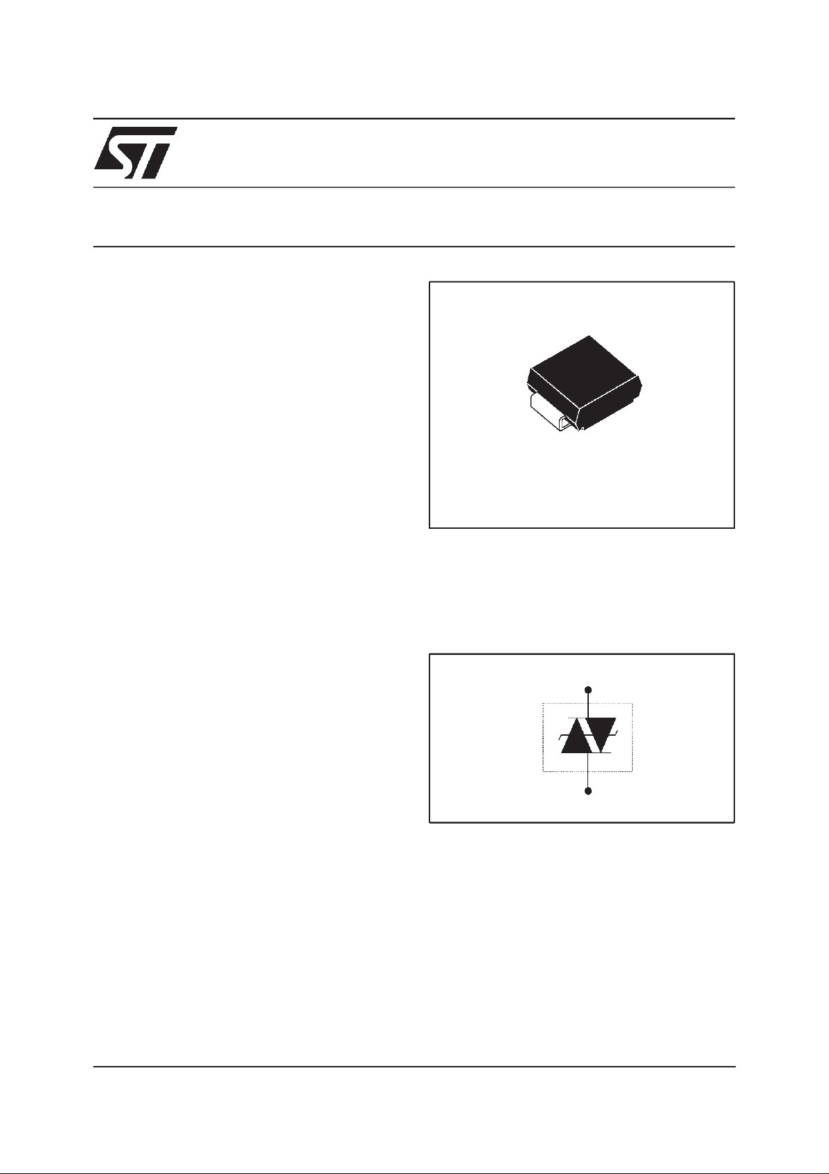
SMP100LC-xxx
TM
FOR HIGH DEBIT RATE
TELECOM LINES PROTECTION
PRELIMINARY DATASHEET
SMB
DESCRIPTION
The SMP100LC-x x x seri es is a very low
capac itance transient surge arrest or designed
for the protec tion of high debit rate
commun i c at ion equipment. It s low capac i t ance
avoid any dist orsion of t he signal. It can also
BENEFITS
n No ageing and no noise
n Short circuit in failure mode, thus still ensuring
protection
n Board space saving
SCHEMATIC DIAGRAM
March 2000 - Ed: 3B
1/8

SMP100LC-xxx
Necessary
Resistor
(note 1)
COMPLIES WITH THE
FOLLOWING STANDARDS:
Peak Surge
Voltage
(V)
Voltage
Waveform
(µs)
Current
Waveform
(µs)
Admissible
Ipp
(A)
ITU-T- K20 4000 10/700 5/310 100 VDE0433 4000 10/700 5/310 100 VDE0878 4000 1.2/50 1/20 100 IEC-1000-4-5 level 4
level 4
FCC Part 68,lightningsurge
type A
FCC Part 68,lightningsurge
1500
800
1000 5/320 5/320 25 -
10/700
1.2/50
10/160
10/560
5/310
8/20
10/160
10/560
100
100
200
100
type B
BELLCORE TR-NWT-001089
First level
BELLCORE TR-NWT-001089
2500
1000
2/10
10/1000
2/10
10/1000
500
100
5000 2/10 2/10 500 -
Second level
CNET I31-24
Note 1: minimum series resistanceto insert on the module line to withstandthe standard.
4000 0.5/700 0.8/310 100 -
THERMAL RESISTANCES
(Ω)
-
-
-
-
-
-
Symbol Parameter Value Unit
R
R
th(j-I)
th(j-a)
Junction to leads
Junction to ambient on printed circuit
20 °C/W
100 °C/W
(with standard footprint dimensions)
ABSOLUTE MAXIMUM RATINGS (T
= 25°C, unless otherwisespecified)
amb
Symbol Parameter Value Unit
I
pp
I
FS
I
TSM
T
L
T
stg
Tj
Note 2: infail safe mode, thedevice acts as a short circuit.
Repetitive peak pulse current:
10/1000 µs (open circuit voltage wave shape 1 kV 10/1000 µs)
8/20 µs (open circuit voltage wave shape 4 kV 1.2/50 µs)
5/310 µs (open circuit voltage wave shape 5 kV 10/700 µs)
2/10 µs (open circuit voltage wave shape 2.5 kV 2/10 µs)
100
250
150
500
Fail-safe mode : maximum current (note 2) 8/20 µs5kA
Non repetitive surgepeak on-statecurrent
One cycle
Non repetitive surgepeak on-statecurrent
F = 50Hz
50Hz
60Hz
0.2s
2s
50
53
23
10
Maximum lead temperature for soldering during 10s 260 °C
Storage temperature range
Maximum junction temperature
- 55 to + 150
150
A
A
A
A
A
A
A
A
°C
°C
2/8
SMP100LC-xxx
Pulse waveform:
10 / 1000 µstr=10µs tp = 1000 µs
8/20µstr=8µstp=20µs
5 / 310 µstr=5µs tp = 310 µs
1/20µstr=1µstp=20µs
2/10µstr=2µstp=10µs
ELECTRICALCHARACTERISTICS(T
Symbol Parameter
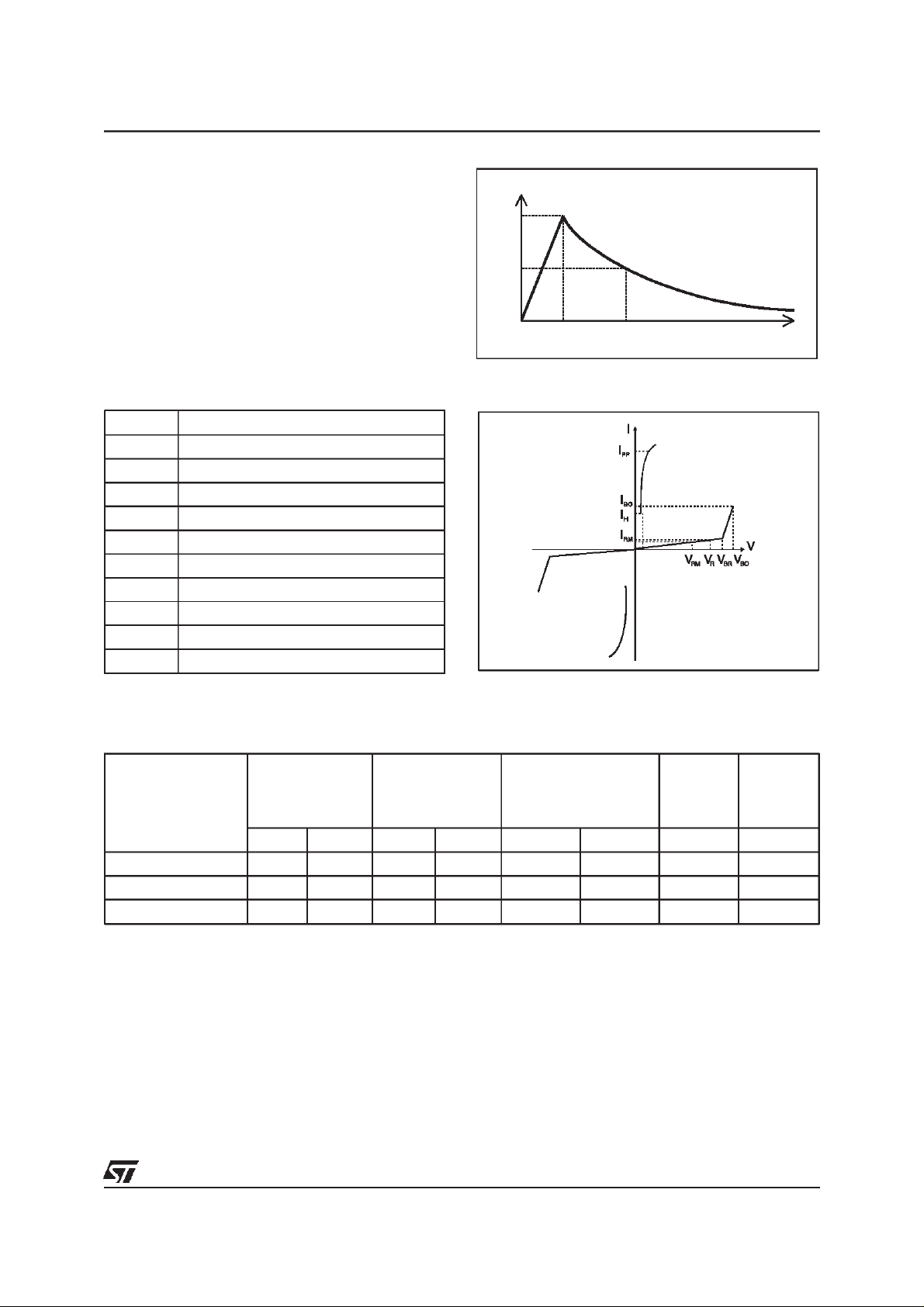
V
RM
I
RM
V
R
I
R
V
BR
V
BO
I
H
I
BO
I
PP
Stand-off voltage
Leakage current at V
RM
Continuous reverse voltage
Leakage current
Breakdown voltage
Breakover voltage
Holding current
Breakover current
Peak pulse current
C Capacitance
amb
=25°C)
%I
100
50
0
PP
t
rp
t
t
DYNAMIC PARAMETERS
Type
IRM@V
max.
RM
IR@V
max.
Note 1
R
VBO@I
BO
max.
Note 2
I
H
min.
Note 3
µAVµAV V mA mA pF
SMP100LC-140 2 120 50 140 185 800 150 30
SMP100LC-200 2 170 50 200 265 800 150 30
SMP100LC-270
Note 1: IRmeasured at VRguarantee VBR>V
Note 2: V
Note 3: See functional holding current testcircuit 1
Note 4: VR=50V bias, V
= 100V/µS, di/dt <10 A/µs, IPP= 100A
RISE
V
= 1kV/µS, di/dt < 10A/µs, IPP= 10A
RISE
VBOparameters are given by a KeyTek ”System2” generator withPN2461 module.
See test circuits 3for VBOdynamic parameters
2 230 50 262 350 800 150 30
R
=1V, F=1MHz.
RMS
C
typ.
Note 4
3/8

SMP100LC-xxx
STATIC PARAMETERS
Symbol Type Test conditions Max. Unit
V
BO
SMP100LC-140 Measured at 50Hz, see test circuit2.
SMP100LC-200 275
In any case V
BOmin
SMP100LC-270 370
Fig 1 : Non repetitive surge peak on-state current
versus overload duration (Tjinitial = 25 °C).
ITSM(A)
70
60
50
40
30
20
10
0
1E-2 1E-1 1E+0 1E+1 1E+2 1E+3
t(s)
F=50Hz
190 V
≥ V
BR
Fig 2 : On-state voltage versus on-state current
(typical values).
IT(A)
50
Tj=25°C
10
1
2.0 2.2 2.4 2.6 2.8 3.0 3.2 3.4 3.6 3.8 4.0
VT(V)
Fig 3 : Relative variation of holding current versus
junction temperature .
IH[Tj] / IH[Tj=25°C]
2.0
1.8
1.6
1.4
1.2
1.0
0.8
0.6
0.4
0.2
0.0
-40 -20 0 20 40 60 80 100 120
Tj(°C)
Fig 4 : Variation of thermal impedance junction to
ambient versus pulse duration (Printed circuit
board FR4, SCu=35µm, recommended pad layout).
Zth(j-a)(°CW)
100
10
1
1E-3 1E-2 1E-1 1E+0 1E+1 1E+2 5E+2
tp(s)
4/8

Fig 5 : Variation of junction capacitance versus reverse voltage applied (typical values).
C [VR] / C [VR=50V]
2.5
2.0
1.5
1.0
0.5
VR(V)
0.0
1 2 5 10 20 50 100 200
SMP100LC-xxx
FUNCTIONAL HOLDING CURRENT(IH) TEST CIRCUIT 1 : GO-NO GO TEST
R
-V
P
V
BAT
D.U.T .
= - 48 V
Surge generator
This is a GO-NO GO test which allows to confirm the holding current (IH) level in a functional test circuit.
TEST PROCEDURE :
- Adjust the current level at the IHvalue by short circuiting the D.U.T.
- Fire the D.U.T. with a surge current : Ipp= 10A, 10/1000 µs.
- The D.U.T. will come back to the off-state within 50 ms max.
5/8

SMP100LC-xxx
TEST CIRCUIT 2 FOR IBOand VBOparameters :
Auto
Transformer
220V/2A
220V
Transformer
220V/800 V
5A
TEST PROCEDURE :
Pulse Test duration (tp = 20ms):
- For Bidirectional devices = Switch K is closed
- For Unidirectional devices = Switch K is open.
V
Selection
OUT
- Device with VBO< 200 Volt
-V
OUT
= 250 V
RMS,R1
- Device with VBO 200 Volt
-V
OUT
= 480 V
RMS,R2
= 240 Ω.
static
relay.
V
out
= 140 Ω.
= 20ms
tp
K
I
BO
measure
R1
140
R2
240
D.U.T
V
BO
measure
TEST CIRCUITS 3 FOR VBODYNAMIC PARAMETERS
100 V /µs, di/dt < 10 A / µs, Ipp = 100 A
2 Ω
U
KeyTek’System 2’ generatorwith PN246I module
10 µF
45 Ω
1kV/µs,di/dt < 10A / µs, Ipp = 10 A
26 µH
U
KeyTek’System 2’ generatorwith PN246I module
60 µF
12 Ω
250 Ω
47 Ω
66 Ω
470 Ω
46 µH
83 Ω
0.36 nF
46 µH
6/8

ORDER CODE
SMP 100 LC - xxx
Trisil Surface Mount
PACKAGE MECHANICAL DATA
SMB (Plastic)
E1
D
E
C
L
SMP100LC-xxx
Low Capacitance
Voltage
I = 100 A
PP
DIMENSIONS
REF.
A1 1.90 2.45 0.075 0.096
A2 0.05 0.20 0.002 0.008
b 1.95 2.20 0.077 0.087
c 0.15 0.41 0.006 0.016
E 5.10 5.60 0.201 0.220
A1
A2
b
E1 4.05 4.60 0.159 0.181
D 3.30 3.95 0.130 0.156
L 0.75 1.60 0.030 0.063
Millimeters Inches
Min. Max. Min. Max.
FOOT PRINT (in millimeters)
2.3
1.52 2.75
1.52
Ordering type Marking Package Weight Base qty Delivery mode
SMP100LC-140 L14 SMB 0.107g. 2500 Tape & Reel
SMP100LC-200 L20 SMB 0.107g 2500 Tape & Reel
SMP100LC-270 L27 SMB 0.107g 2500 Tape & Reel
7/8

SMP100LC-xxx
Information furnishedis believed tobeaccurate and reliable.However, STMicroelectronicsassumes noresponsibility forthe consequencesof
use of suchinformation nor forany infringementof patents orother rightsof third partieswhichmay result fromits use.No license isgranted by
implication or otherwise under any patent or patent rights of STMicroelectronics. Specifications mentioned in this publication are subject to
change without notice. This publicationsupersedes and replaces allinformation previously supplied.
STMicroelectronics products are not authorized for use as critical components in life support devices or systems without express written
approval of STMicroelectronics.
The ST logo is a registered trademark of STMicroelectronics
2000 STMicroelectronics - Printed in Italy - All rights reserved.
STMicroelectronics GROUP OF COMPANIES
Australia -Brazil - China - Finland - France - Germany - Hong Kong - India - Italy - Japan - Malaysia
Malta - Morocco - Singapore - Spain - Sweden - Switzerland - United Kingdom - U.S.A.
http://www.st.com
8/8
 Loading...