

Datasheet SM6HT24A, SM6HT27A, SM6HT30A, SM6HT36A, SM6HT39A Datasheet (SGS Thomson Microelectronics)
...
®
HIGH TEMPERATURE TRANSIL
FOR AUTOMOTIVE APPLICATIONS
FEATURES
HIGH PERFORMANCE TRANSIL DESIGNED
TO FIT HIGH TEMPERATURE ENVIRONMENT
LIKE AUTOMOTIVE APPLICATIONS...
HIGH RELIABILITY P LANA R T ECH NOLO GY
HIGH PERFORMANCE IN VOLTAGE REGU-
LATION MODE
VERY LOW LEAKAGE CU RRENT
max = 5 µA @ Tamb = 150° C)
(I
R
PEAK PULSE POW ER : 600 W (10/1000µs)
FAST RESPONSE TIME
UNIDIRECTIONAL TYPE
LOW CLAMPING FACTOR
DESCRIPTION
This high performance Transil series has been designed to fit high temperature environment such as
automotive applications, using surface mount
technology. These devices are using high reliability
planar technology resulting in high performances
in voltage regulation mode and low leakage current at high temperature.
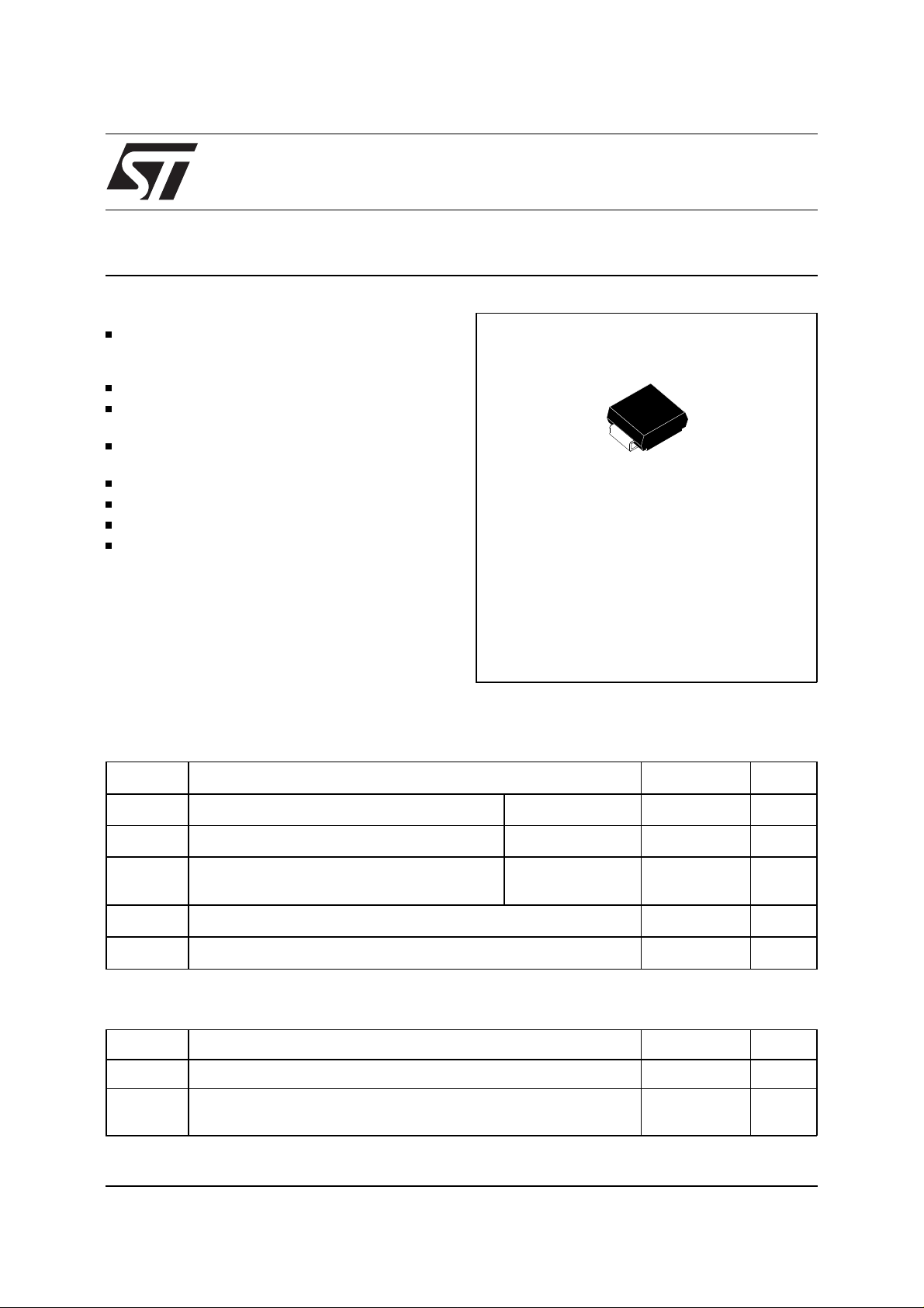
SM6HTxxA
TM
SMB
(JEDEC D0-214AA)
ABSOL UTE M AXIMU M RA TIN GS (T
amb
= 25°C)
Symbol Parameter Value Unit
P
PP
Peak pulse power dissipation (see note 1) Tj initial = T
P Power dissipation on infinite heatsink T
I
FSM
Non repetitive surge peak forward
current for unidirectional types
T
stg, TJ
T
L
Note 1
: For a surge greater than the maximum valu es, the diode wil l fail in short-ci rcuit.
Storage and operating junction temperature range
Maximum lead temperature for soldering during 10 s.
tp = 10ms
Tj initial = T
amb
50°C5W
amb =
amb
600 W
75 A
- 65 to 175 °C
260 °C
THERMAL RESISTANCES
Symbol Parameter Value Unit
R
R
th (j-l)
th (j-a)
Junction to leads
Junction to ambient on printed circuit.
20 °C/W
100 °C/W
On recommended pad layout
April 1999 Ed: 4A
1/5
SM6HTxxA
ELECTRICAL CHARACTERISTICS
(T
= 25°C unless otherwise specified)
amb
Symbol Parameter
V
RM
V
BR
V
CL
I
RM
I
PP
V
F
Types Marking IRM @ V
SM6HT24A
SM6HT27A
SM6HT30A
SM6HT36A
SM6HT39A
SM6HT43A
Note 2 :
Pulse test : tp < 50 ms
Note 3 :
∆VBR = αT x (Tamb - 25) x VBR (25°C)
Stand-off voltage
Breakdown voltage
Clamping voltage
Leakage current @ V
Peak pulse current
Forward voltage drop
< 3.5V @ IF = 50A
V
F
(pulse test: tp ≤ 500µs)
Tamb=25°C Tamb=150°C note2 10/1000µsmax
max max min nom max max note 3
A
µ
EMB 2 5 20.5 22.8 24 25.2 1 33.2 18.0 9.4
EPB 2 5 23.1 25.7 27 28.4 1 37.5 16.0 9.6
ERB 2 5 25.6 28.5 30 31.5 1 41.5 14.5 9.7
EVB 2 5 30.8 34.2 36 37.8 1 49.9 12.0 9.9
EXB 2 5 33.3 37.1 39 41.0 1 53.9 11.1 10.0
EYB 2 5 36.8 40.9 43 45.2 1 59.3 10.1 10.1
I
I
F
VV
CLVBR
V
RM
RM
RM
A VVVVmAVA10
µ
VBR @ I
R
I
I
RM
PP
V
F
VCL @ I
PP
V
T
α
-4
/°C
2/5

SM6HTxxA
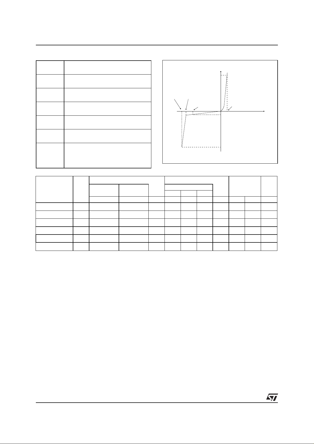
Fig. 1-1: Peak power dissipation versus initial junc-
tion temperature.
Ppp[Tj initial] / Pp p [T j initial=25°C]
1.1
1.0
0.9
0.8
0.7
0.6
0.5
0.4
0.3
0.2
0.1
0.0
0 25 50 75 100 125 150 175 200
Tj initial(°C)
Fig. 2: Peak pulse power versus exponential pulse
duration (Tj initial=25°C).
Ppp(kW)
10.0
1.0
0.1
0.01 0.10 1.00 10.00
tp(ms)
Fig. 1-2: Continous power dissipation versus ambient temperature.
P(W)
6
Rth(j-a)=Rth(j-l)
5
4
3
2
Rth(j-a)=100°C/W
1
0
0 25 50 75 100 125 150 175
Tamb(°C)
Fig. 3: Clamping voltage versus peak pulse current (Tj initial=25°C).
Ipp(A)
1E+2
SM6HT27A
SM6HT24A
1E+1
1E+0
tp=1ms
1E-1
10 100
Vcl(V)
SM6HT30A
SM6HT36A
SM6HT39A
tp=20µs
SM6HT43A
Fig. 4: Junction capacitance versus reverse applied voltage (typical values).
C(pF)
1000
500
SM6HT24A
SM6HT27A
200
100
1 10 100 200
VR(V)
SM6HT30A
SM6HT36A
SM6HT43A
F=1MHz
SM6HT39A
Fig. 5: Peak forward voltage drop versus peak forward current (typical values).
IFM(A)
100.0
Tj=175°C
10.0
Tj=25°C
1.0
0.1
0.5 1.0 1.5 2.0 2.5 3.0 3.5
VFM(V)
3/5

SM6HTxxA
Fig. 6: Variation of thermal impedance junction to
ambient versus pulse duration (Printed circuit
board FR4 with recommended pad layout).
Zth(j-a)(°C/W)
1E+2
1E+1
1E+0
1E-1
1E-3 1E-2 1E-1 1E+0 1E+1 1E+2 5E+2
tp(s)
Fig .8: Variation of leakage current versus junction
temperature (typical values).
IR(µA)
1E+4
1E+3
1E+2
1E+1
1E+0
1E-1
1E-2
1E-3
1E-4
25 50 75 100 125 150 175
Tj(°C)
Fig. 7: Thermal resistance junction to ambient versus copper surface under each lead (printed circuit
board FR4, e(Cu)=35µm).
Rth(j-a) (°C/W)
100
90
80
70
60
50
40
012345
S(cm²)
4/5

MARKING : Logo, Date Code, Type Code, Cathode Band.
PACKAGE ME CHANICAL D AT A
SMB (Plastic)
E1
D
SM6HTxxA
DIMENSIONS
REF.
A1 1.90 2.45 0.075 0.096
A2 0.05 0.20 0.002 0.008
Millimeters Inches
Min. Max. Min. Max.
E
A1
C
L
A2
Weight = 0.107 g
FOOTPRINT DIMENSIONS (Millimeter)
SMB Plast ic.
2.3
Packaging
1.52 2.75
: standard packaging is tape and reel.
1.52
b 1.95 2.20 0.077 0.087
c 0.15 0.41 0.006 0.016
E 5.10 5.60 0.201 0.220
E1 4.05 4.60 0.159 0.181
b
D 3.30 3.95 0.130 0.156
L 0.75 1.60 0.030 0.063
Information furnished is believed to be accurate and reliable. However, STMicroelectronics assumes no responsibility for the consequences of
use of such information nor for any infringement of patents or other rights of third parties which may result from its use. No license is granted by
implication or oth erwise under any patent or patent rights of STMi croelectronics . Specifications mentioned i n this publication are subjec t to
change without notice. This publication supersedes and replaces all information previously supplied.
STMicroelectr oni cs products are not authorized for use as critical components in l i fe s upport devices or s ystems without express written approval of STMicroelectronics.
The ST logo is a registered trademark o f STMicroelectron ics
© 1999 STMicroelectronics - Printed in Italy - All rights reserved.
STMicroelectronics GROUP OF COMPANIES
Australia - Brazil - Canada - China - France - Germany - Italy - Japan - Korea - Malaysia - Malta - Mexico - Morocco -
The Netherlands - Singapore - Spain - Sweden - Switzerland - Taiwan - Thailand - United Kingdom - U.S.A.
http://www.st.com
5/5
 Loading...