

HIGH VOLTAGE FAST-SWITCHING
■ SGSIF344IS SGS-THOMSONPREFERRED
SALESTYPE
■ HIGH VOLTAGE CAPABILITY
■ VERYHIGH SWITCHING SPEED
■ LOW BASE-DRIVEREQUIREMENTS
APPLICATIONS:
■ SWITCHMODE POWER SUPPLIES
■ HORIZONTAL DEFLECTION FOR COLOUR
TVS AND MONITORS
SGSIF344
SGSIF444
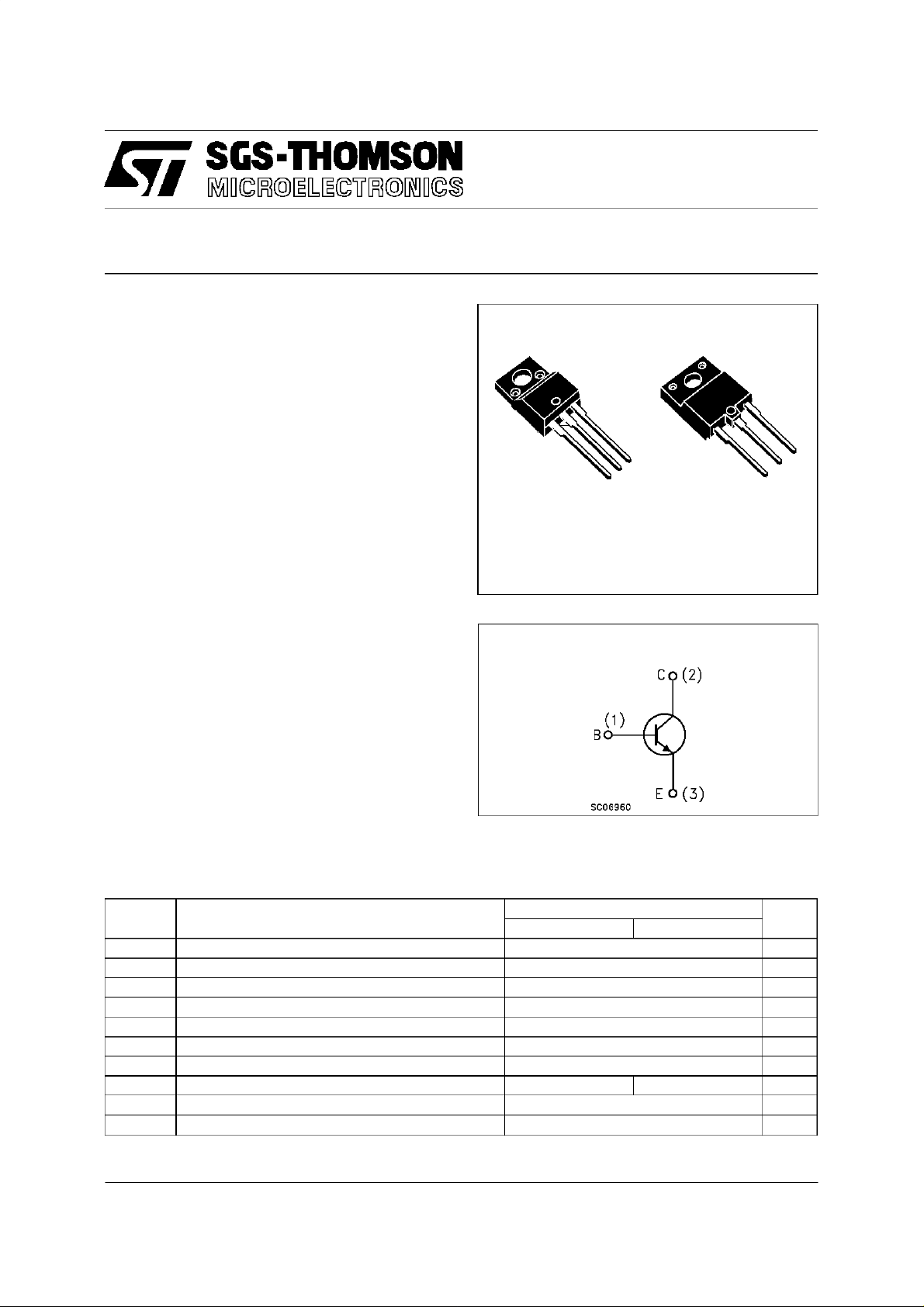
NPN POWER TRANSISTORS
3
2
1
3
2
1
DESCRIPTION
The SGSIF344and SGSIF444 are manufactured
ISOWATT220 ISOWATT218
using Multiepitaxial Mesa technology for
cost-effective high performance and uses a
Hollow Emitter structure to enhance switching
speeds.
These transistors are available in ISOWATT220
and ISOWATT218plasticpackagerespectively.
INTERNAL SCHEMATIC DIAGRAM
The SGSF series is designed for high speed
switching applications such as power supplies
and horizontal deflection circuits in TVs and
monitors.
ABSOLUTE MAXIMUM RATINGS
Symb o l Parameter Value Uni t
SGS I F 344 SGS I F444
V
V
V
I
I
P
T
Collector-Emitte r Voltage ( VBE= 0 ) 1200 V
CES
Collector-Emitte r Voltage ( IB= 0 ) 600 V
CEO
Emit t er-Bas e Volt age (IC=0) 7 V
EBO
I
Collector Current 7 A
C
Collector Peak Current (tp<5ms) 12 A
CM
I
Base Current 5 A
B
Base Peak Curr ent ( tp<5ms) 8 A
BM
Total Dissipation at Tc=25oC4050W
tot
St orage T emperatu re -65 to 15 0
stg
T
Max. Oper a ti ng Jun c t ion T em perature 150
j
o
C
o
C
June 1997
1/7
SGSIF344 / SGSIF444
THERMAL DATA
R
thj-case
Ther mal Res istance Junct ion-cas e Max 3.12 2.5
ISOWAT T220 I SOW ATT218oC/W
o
C/W
ELECTRICAL CHARACTERISTICS (T
=25oC unlessotherwise specified)
case
Symbol Parameter Test Condition s Min. Typ. Max. Unit
I
CES
I
CEO
I
EBO
V
CEO(sus)
Collector Cut-off
Current (V
BE
=0)
Collector Cut-off
Current (I
B
=0)
Emit ter Cut -off Current
=0)
(I
C
∗ Collector-Emitter
V
= 1200 V 200 µA
CE
=380V
V
EC
V
=600V
EC
V
=7V 1 mA
BE
200
2
IC= 10 0 mA 600 V
Sust aining Voltag e
V
CE(sat)
V
BE(sat)
∗ Collect or- Emitter
Saturation Voltage
∗ Base-Emitt er
Saturation Voltage
t
ON
t
t
ON
t
s
t
f
s
t
f
Turn-on Time
St orage Time
Fall T ime
Turn-on Time
St orage Time
Fall T ime
IC=3.5A IB=0.7A
=2.5A IB=0.35A
I
C
IC=3.5A IB=0.7A
=2.5A IB=0.35A
I
C
RESI STIVE LOAD
=250v IC=3.5A
v
CC
I
=0.7A IB1=-1.4A
B1
RESI STIVE LOAD
=250v IC=3.5A
v
CC
=0.7A IB1=-1.4A
I
B1
0.7
2.2
0.18
0.7
1.5
0.2
1.5
1.5
1.5
1.5
1.2
3.5
0.4
With Antisaturation Network
0.7
1
0.2
1.4
0.1
2.8
0.2
4
0.3
s
t
f
s
t
f
s
t
f
Turn-on Time
St orage Time
Fall T ime
St orage Time
Fall T ime
St orage Time
Fall T ime
t
ON
t
t
t
∗
Pulsed: Pulse duration = 300 µs, duty cycle 1.5 %
RESI STIVE LOAD
=250V IC=3.5A
V
CC
=0.7A VBE(off) = - 5 V
I
B1
INDUCTIV E LOAD
=3.5A hFE=5
I
C
= 450 V V
V
CL
L = 300 µ HR
BE(of f)
BB
=-5V
=1.2Ω
INDUCTIV E LOAD
=3.5A hFE=5
I
C
= 450 V V
V
CL
L = 300 µ HR
= 100oC
T
c
BE(of f)
BB
=-5V
=1.2Ω
µA
mA
V
V
V
V
µs
µs
µs
µs
µs
µs
µs
µs
µs
µs
µs
µs
µs
2/7
SGSIF344 / SGSIF444
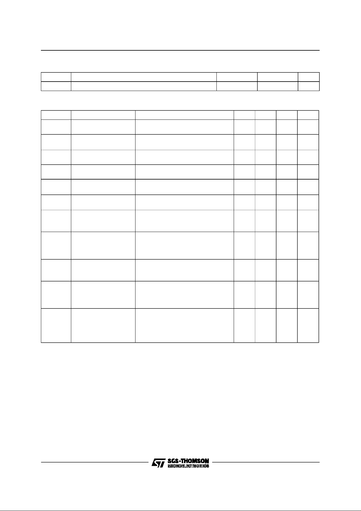
Safe Operating Area
Derating Curve
ReverseBiasedSOA
DC Current Gain
CollectorEmitter Saturation Voltage
BaseEmitter Saturation Voltage
3/7
SGSIF344 / SGSIF444
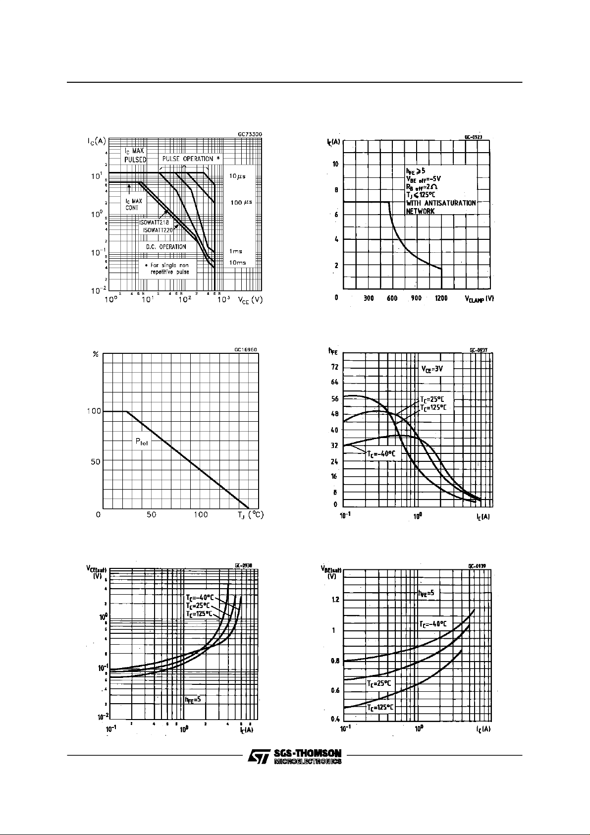
ResistiveLoad Switching Times InductiveLoad SwitchingTimes
SwitchingTimesPercentanceVariation
4/7

ISOWATT220MECHANICAL DATA
SGSIF344 / SGSIF444
DIM.
MIN. TYP. MAX. MIN. TYP. MAX.
A 4.4 4.6 0.173 0.181
B 2.5 2.7 0.098 0.106
D 2.5 2.75 0.098 0.108
E 0.4 0.7 0.015 0.027
F 0.75 1 0.030 0.039
F1 1.15 1.7 0.045 0.067
F2 1.15 1.7 0.045 0.067
G 4.95 5.2 0.195 0.204
G1 2.4 2.7 0.094 0.106
H 10 10.4 0.393 0.409
L2 16 0.630
L3 28.6 30.6 1.126 1.204
L4 9.8 10.6 0.385 0.417
L6 15.9 16.4 0.626 0.645
L7 9 9.3 0.354 0.366
Ø 3 3.2 0.118 0.126
mm inch
E
A
D
B
L3
L6
L7
¯
F1
F
G1
H
G
F2
123
L2
L4
P011G
5/7

SGSIF344 / SGSIF444
ISOWATT218MECHANICAL DATA
DIM.
MIN. TYP. MAX. MIN. TYP. MAX.
mm inch
A 5.35 5.65 0.210 0.222
C 3.3 3.8 0.130 0.149
D 2.9 3.1 0.114 0.122
D1 1.88 2.08 0.074 0.081
E 0.75 1 0.029 0.039
F 1.05 1.25 0.041 0.049
G 10.8 11.2 0.425 0.441
H 15.8 16.2 0.622 0.637
L1 20.8 21.2 0.818 0.834
L2 19.1 19.9 0.752 0.783
L3 22.8 23.6 0.897 0.929
L4 40.5 42.5 1.594 1.673
L5 4.85 5.25 0.190 0.206
L6 20.25 20.75 0.797 0.817
M 3.5 3.7 0.137 0.145
N 2.1 2.3 0.082 0.090
U 4.6 0.181
L3
N
E
A
C
L2
D
D1
6/7
L5
M
H
L6
F
U
G
123
L1
L4
P025C

SGSIF344 / SGSIF444
Informationfurnished is believed to be accurate and reliable.However, SGS-THOMSON Microelectronics assumes no responsabilityfor the
consequencesof use of such informationnor for any infringementof patents or other rights of third parties which may results from its use. No
license is granted byimplicationor otherwise under anypatentor patentrights of SGS-THOMSONMicroelectronics. Specificationsmentioned
in this publicationare subject tochange without notice. This publicationsupersedes and replacesall informationpreviously supplied.
SGS-THOMSON Microelectronicsproducts are notauthorizedfor useascritical components inlifesupportdevicesor systemswithout express
written approvalof SGS-THOMSONMicroelectonics.
1997 SGS-THOMSON Microelectronics -Printed in Italy- All RightsReserved
Australia- Brazil - Canada- China- France- Germany- Hong Kong - Italy - Japan- Korea- Malaysia -Malta - Morocco - The Netherlands-
Singapore - Spain- Sweden - Switzerland - Taiwan - Thailand - UnitedKingdom - U.S.A
SGS-THOMSON MicroelectronicsGROUP OF COMPANIES
...
7/7
 Loading...