

SG2525A
REGULATINGPULSE WIDTHMODULATORS
.
8 TO35 V OPERATION
.5.1V REFERENCETRIMMED TO
.
100Hz TO 500KHzOSCILLATORRANGE
±
1%
.SEPARATEOSCILLATORSYNCTERMINAL
.
ADJUSTABLEDEADTIMECONTROL
.INTERNALSOFT-START
.PULSE-BY-PULSESHUTDOWN
.INPUT UNDERVOLTAGE LOCKOUT WITH
HYSTERESIS
.
LATCHING PWM TO PREVENT MULTIPLE
PULSES
.
DUALSOURCE/SINKOUTPUT DRIVERS
DES CRIPTION
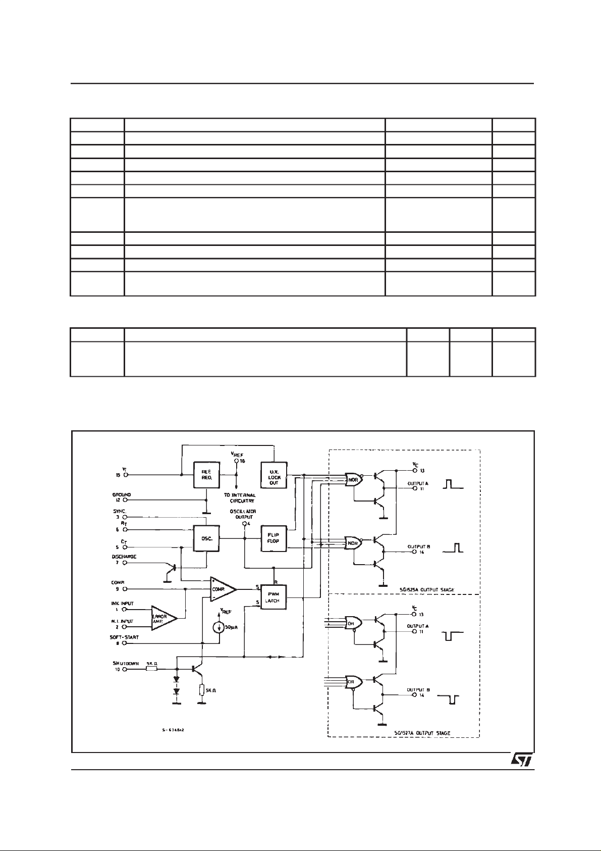
The SG3525Aseriesof pulse widthmodulatorintegrated circuitsare designed to offerimprovedperformance and lowered external parts count when
used indesigningalltypesof switchingpower supplies.Theon-chip+5.1 V referenceistrimmedto±
1 % andthe inputcommon-moderangeoftheerror
amplifierincludesthereferencevoltageeliminating
externalresistors. A sync inputto the oscillatorallowsmultipleunitstobeslavedor a singleunittobe
synchronizedto an externalsystemclock. A single
resistorbetweentheC
provide a wide range of dead time ad- justment.
Thesedevicesalsofeaturebuilt-insoft-startcircuitry
with only an external timing capacitor required. A
shutdownterminalcontrolsboththesoft-startcircuity and the output stages, providing instantaneous
andthedischargeterminals
T
SG3525A
DIP16 16( Na rr ow)
turn off through the PWM latch with pulsed shutdown,as wellassoft-startrecyclewithlongershutdowncommands.Thesefunctionsarealsocontrolledbyanundervoltagelockoutwhichkeepstheoutputs off and the soft-startcapacitordischarged for
sub-normalinputvoltages.Thislockoutcircuitryincludesapproximately500 mVof hysteresisforjitterfree operation. Another featureof these PWM circuits is a latch following the comparator. Once a
PWM pulses has been terminated for any reason,
theoutputswill remainoff for thedurationoftheperiod. The latch is reset with each clock pulse. The
output stages are totem-pole designs capable of
sourcing or sinking in excess of 200 mA. The
SG3525AoutputstagefeaturesNORlogic,givinga
LOWoutputfor anOFFstate.
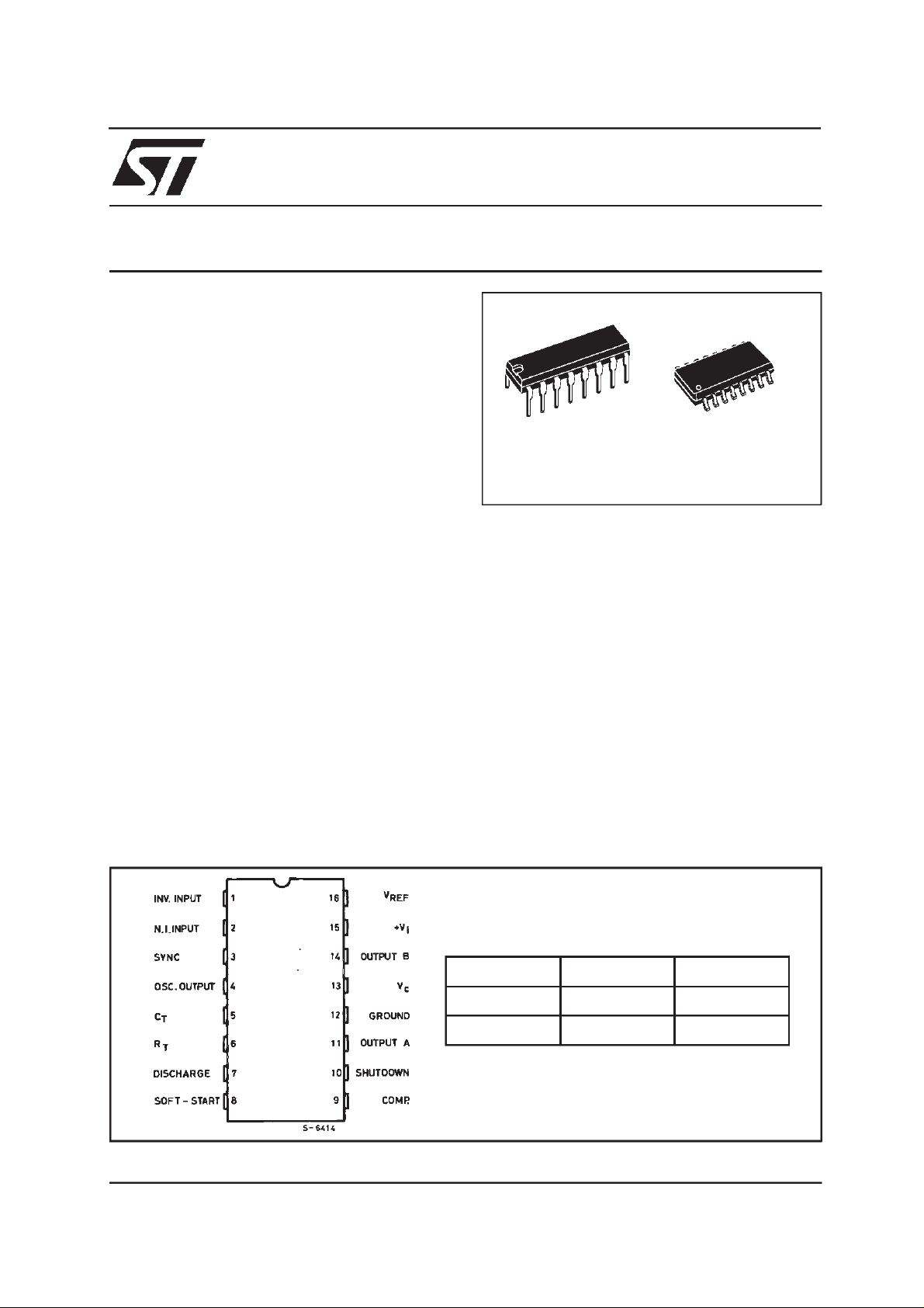
PI N CO NNECTI O N S AND ORDE RING NUMBERS (top view)
Type Plastic DIP SO16
SG2525A SG2525AN SG2525AP
SG3525A SG3525AN SG3525AP
June 2000
1/12
SG2525A-SG3525A
ABSOLUTEMAXIMUMRATINGS
Symbol Parameter Value Unit
V
V
I
OSC
I
o
I
R
I
T
P
tot
T
T
stg
T
op
THERMAL DATA
Symbol Parameter SO16 DIP16 Unit
R
th j-pins
R
th j-amb
R
th j-alumina
*
Thermalresistancejunction-aluminawiththe devicesolderedon themiddleofanaluminasupportingsubstratemeasuring15× 20mm; 0.65mm
thickness withinfiniteheatsink.
Supply Voltage 40 V
i
Collector Supply Voltage 40 V
C
Oscillator Charging Current 5 mA
Output Current, Source or Sink 500 mA
Reference Output Current 50 mA
Current through CTTerminal
Logic Inputs
Analog Inputs
Total Power Dissipation at T
Junction Temperature Range – 55 to 150
j
=70°C 1000 mW
amb
5
– 0.3 to + 5.5
– 0.3 to V
Storage Temperature Range – 65 to 150
Operating Ambient Temperature : SG2525A
SG3525A
–25to85
0to70
Thermal Resistance Junction-pins Max
Thermal Resistance Junction-ambient Max
Thermal Resistance Junction-alumina (*) Max 50
i
50
80
°C/W
°
°C/W
mA
V
V
C
°
C
°
C
°
°C
C/W
BLOCK DI AGRAM
2/12
ELECTRICALCHARACTERISTICS
(V# i = 20 V, andoveroperatingtemperature, unlessotherwisespecified)
SG2525A-SG3525A
Symbol Parameter Test Conditions
SG2525A SG3525A
Unit
Min. Typ. Max. Min. Typ. Max.
REFERENCE SECTION
V
V
∆
∆V
V
∆
REF
Output Voltage Tj=25°C 5.05 5.1 5.15 5 5.1 5.2 V
REF
Line Regulation Vi= 8 to 35 V 10 20 10 20 mV
REF
Load Regulation IL= 0 to 20 mA 20 50 20 50 mV
REF
/∆T* Temp. Stability Over Operating Range 20 50 20 50 mV
* Total Output Variation Line, Load and
5 5.2 4.95 5.25 V
Temperature
Short Circuit Current V
* Output Noise Voltage 10 Hz≤f≤10 kHz,
∆V
* Long Term Stability Tj= 125 °C, 1000 hrs 20 50 20 50 mV
REF
=0Tj=25°C 80 100 80 100 mA
REF
40 200 40 200µVrms
=25°C
T
j
OSCILLATOR SECTION * *
*, • Initial Accuracy T
*,
Voltage Stability V
•
=25°C ±2 ±6 ±2 ±6%
j
= 8 to 35 V
i
0.3
±
1
±
1
±
2%
±
∆f/∆T* Temperature Stability Over Operating Range ± 3 ± 6 ± 3 ± 6%
f
MIN
f
MAX
Minimum Frequency RT= 200 KΩ CT= 0.1µF 120 120 Hz
Maximum Frequency RT=2KΩCT= 470 pF 400 400 KHz
Current Mirror I
= 2 mA 1.7 2 2.2 1.7 2 2.2 mA
RT
*, • Clock Amplitude 3 3.5 3 3.5 V
*,
Clock Width T
•
=25°C 0.3 0.5 1 0.3 0.5 1
j
s
µ
Sync Threshold 1.2 2 2.8 1.2 2 2.8 V
Sync Input Current Sync Voltage = 3.5 V 1 2.5 1 2.5 mA
ERROR AMPLIFIER SECTION (V
V
I
Input Offset Voltage 0.5 5 2 10 mV
OS
Input Bias Current 1 10 1 10
I
b
Input Offset Current 1 1 µA
os
DC Open Loop Gain R
* Gain Bandwidth
= 5.1 V)
CM
≥ 10 MΩ 60 75 60 75 dB
L
= 0 dB Tj=25°C1 2 1 2 MHz
G
v
A
µ
Product
*, ❚ DC Transconduct. 30 KΩ ≤ R
=25°C
T
j
≤ 1MΩ
L
1.1 1.5 1.1 1.5 ms
Output Low Level 0.2 0.5 0.2 0.5 V
Output High Level 3.8 5.6 3.8 5.6 V
CMR Comm. Mode Reject. V
PSR Supply Voltage
= 1.5 to 5.2 V 60 75 60 75 dB
CM
= 8 to 35 V 50 60 50 60 dB
V
i
Rejection
3/12
SG2525A-SG3525A
ELECTRICAL CHARACTERISTICS
Symbol Parameter Test Conditions
(continued)
SG2525A SG3525A
Min. Typ. Max. Min. Typ. Max.
PWM COMPARATOR
Minimum Duty-cycle 0 0 %
• Maximum Duty-cycle 45 49 45 49 %
Input Threshold Zero Duty-cycle 0.7 0.9 0.7 0.9 V
•
Maximum Duty-cycle 3.3 3.6 3.3 3.6 V
* Input Bias Current 0.05 1 0.05 1 µA
SHUTDOWN SECTION
Soft Start Current V
Soft Start Low Level V
Shutdown Threshold To outputs, V
Shutdown Input Current V
* Shutdown Delay V
OUTPUT DRIVERS (each output) (V
Output Low Level I
Output High Level I
Under-Voltage Lockout V
Collector Leakage VC= 35 V 200 200
I
C
t
* Rise Time CL= 1 nF, Tj=25°C 100 600 100 600 ns
r
* Fall Time CL= 1 nF, Tj=25°C 50 300 50 300 ns
t
f
= 0 V, VSS=0V 255080255080 µA
SD
= 2.5 V 0.4 0.7 0.4 0.7 V
SD
= 5.1 V
=25°C
T
j
= 2.5 V 0.4 1 0.4 1 mA
SD
= 2.5 V Tj=25°C 0.2 0.5 0.2 0.5 µs
SD
=20V)
C
= 20 mA 0.2 0.4 0.2 0.4 V
sink
I
= 100 mA 1 2 1 2 V
sink
=20mA 1819 1819 V
source
= 100 mA 17 18 17 18 V
I
source
and Vss= High 6 7 8 6 7 8 V
comp
SS
0.6 0.8 1 0.6 0.8 1 V
TOTAL STANDBY CURRENT
Supply Current Vi= 35 V 14 20 14 20 mA
I
s
Unit
µ
A
*
These parameters, althoughguaranteed over therecommended operating conditions, are not 100% tested inproduction.
•
Testedat f
f=
DC transconductance (gM) relatesto DCopen-loopvoltagegain (Gv) according tothefollowingequation: Gv=gMRLwhereRListhe resistance
.
frompin 9 to ground. Theminimumg
=40 KHz (RT= 3.6 KΩ,CT=10nF, RD=0Ω). Approximateoscillatorfrequency is defined by:
osc
1
C
(0.7 RT+3RD)
T
specification is used to calculateminimum Gvwhenthe error amplifieroutput is loaded.
M
4/12

TEST CI RCUIT
SG2525A-SG3525A
5/12

SG2525A-SG3525A
RECOMMENDED OPERATINGCONDITIONS (•)
Parameter Value
Input Voltage (V
Collector Supply Voltage (V
Sink/Source Load Current (steady state) 0 to 100 mA
Sink/Source Load Current (peak) 0 to 400 mA
Reference Load Current 0to20mA
Oscillator Frequency Range 100 Hz to 400 KHz
Oscillator Timing Resistor 2 KΩ to 150 KΩ
Oscillator Timing Capacitor 0.001µF to 0.1µF
Dead Time Resistor Range 0 to 500
• (
Range over whichthe device is functionaland parameterlimits areguaranteed.
⋅)
) 8to35V
i
) 4.5 to 35 V
C
Ω
Figure 1 :
Oscillator Charge Time vs. R
and C
.
T
Figure 3 :OutputSaturation
Characteristics.
T
Figure 2 :
Oscilla tor Discharge Time vs. R
and C
.
T
D
Figure4 : Error AmplifierVoltageGain and
Phasevs. Frequency.
6/12

SG2525A-SG3525A
Figure5
: ErrorAmplifier.
PRINCIPLES OF OPERATION
SHUTDOWN OPTIONS(see Block Diagram)
Since both the compensation and soft-starttermi-
nals (Pins 9 and 8) have current source pull-ups,
either canreadily accept a pull-down signal which
onlyhastosinka maximumof100
µA
toturnoffthe
outputs.Thisissubjecttotheadded requirementof
dischargingwhateverexternalcapacitancemay be
attachedto thesepins.
Analternateapproachistheuseoftheshutdowncircuitry of Pin 10 which has been improved to enhance the available shutdown options. Activating
this circuit by applying a positive signal on Pin 10
performstwo functions: the PWM latch isimmedi-
ately set providing the fastestturn-offsignal to the
outputs ; and a 150 µA current sinkbegins to dischargethe externalsoft-startcapacitor.If the shutdown command is short, the PWM signal is terminated without significantdischarge of thesoft-start
capacitor,thus,allowing,forexample,a convenient
implementation of pulse-by-pulse current limiting.
HoldingPin 10highfora longerduration,however,
will ultimatelydischarge this external capacitor,recyclingslow turn-on uponrelease.
Pin 10 should not be left floating as noise pickup
couldconceivablyinterruptnormaloperation.
7/12

SG2525A-SG3525A
Figure 6
: OscillatorSchematic.
Figure7:
Output Circuit (1/2 circuit shown).
8/12

SG2525A-SG3525A
Figure 8. Figure 9
For single-ended supplies, the driver outputs are
grounded.The V
terminalisswitched to groundby
C
thetotem-polesourcetransistorsonalternateoscillatorcycles.
In conventionalpush-pull bipolar designs, forward
base drive is controlled by R1-R3. Rapid turn-off
times for the power devices are achieved with
speed-upcapacitorsC
.
andC2.
1
Figure 1 0. Figure 1 1.
Thelowsourceimpedanceoftheoutputdriversprovides rapid charging of Power Mos input capacitancewhile minimizing externalcomponents.
Low power transformers can be driven directly.
Automaticresetoccursduringdeadtime,whenboth
endsof theprimarywindingareswitchedtoground.
9/12

SG2525A-SG3525A
DIM.
MIN. TYP. MAX. MIN. TYP. MAX.
a1 0.51 0.020
B 0.77 1.65 0.030 0.065
b 0.5 0.020
b1 0.25 0.010
D 20 0.787
E 8.5 0.335
e 2.54 0.100
e3 17.78 0.700
F 7.1 0.280
I 5.1 0.201
L 3.3 0.130
Z 1.27 0.050
mm inch
OUTLINE AND
MECHANICAL DATA
DIP16
10/12

SG2525A-SG3525A
DIM.
MIN. TYP. MAX. MIN. TYP. MAX.
A 1.75 0.069
a1 0.1 0.25 0.004
a2 1.6 0.063
b 0.35 0.46 0.014 0.018
b1 0.19 0.25 0.007 0.010
C 0.5 0.020
c1 45°(typ.)
D (1) 9.8 10 0.386 0.394
E 5.8 6.2 0.228 0.244
e 1.27 0.050
e3 8.89 0.350
F (1) 3.8 4 0.150 0.157
G 4.6 5.3 0.181 0.209
L 0.4 1.27 0.016 0.050
M 0.62 0.024
S
mm inch
0.009
8°(max.)
OUTLINE AND
MECHANICAL DATA
SO16 Narrow
(1) D andF do not includemold flashor protrusions. Moldflash or potrusions shall not exceed 0.15mm (.006inch).
11/12

SG2525A-SG3525A
Information furnished is believed to be accurate and reliable. However, STMicroelectronics assumes no responsibility for the consequences of use of such information nor for any infringement of patents or other rights of third parties which may result from its use. No
license is granted by implication or otherwise under any patent or patent rights of STMicroelectronics. Specification mentioned in this
publication are subject to change without notice. This publication supersedes and replaces all information previously supplied. STMicroelectronics products are not authorized for use as critical components in life support devices or systems without express written
approval of STMicroelectronics.
Australia - Brazil - China - Finland - France - Germany - Hong Kong - India - Italy - Japan - Malaysia - Malta - Morocco -
The ST logo is a registered trademark of STMicroelectronics
2000 STMicroelectronics – Printed in Italy – All Rights Reserved
STMicroelectronics GROUP OF COMPANIES
Singapore - Spain - Sweden - Switzerland - United Kingdom - U.S.A.
http://www.st.com
12/12
 Loading...