

TL7700A Series
April 2000
SUPPLY VOLTAGE SUPERVISORS
.POWER-ONRESETGENERATOR
.AUTOMATIC RESET GENERATION AFTER
VOLTAGEDROP
.
WIDE SUPPLY VOLTAGE RANGE ... 3V TO
18V
.
PRECISIONVOLTAGESENSOR
.TEMPERATURE-COMPENSATED VOLTAGE
REFERENCE
.
TRUEANDCOMPLEMENTRESETOUTPUTS
.EXTERNALLYADJUSTABLEPULSE WIDTH
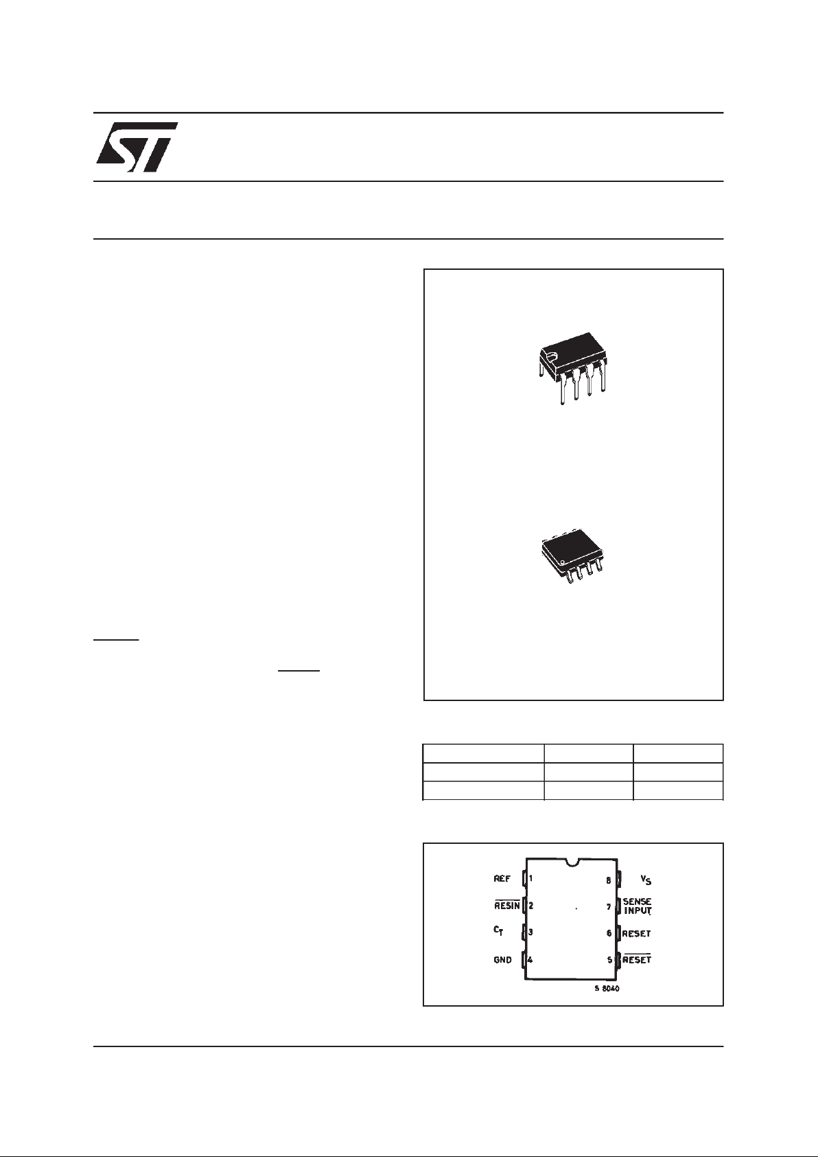
N
Minidip
DESCRIPTION
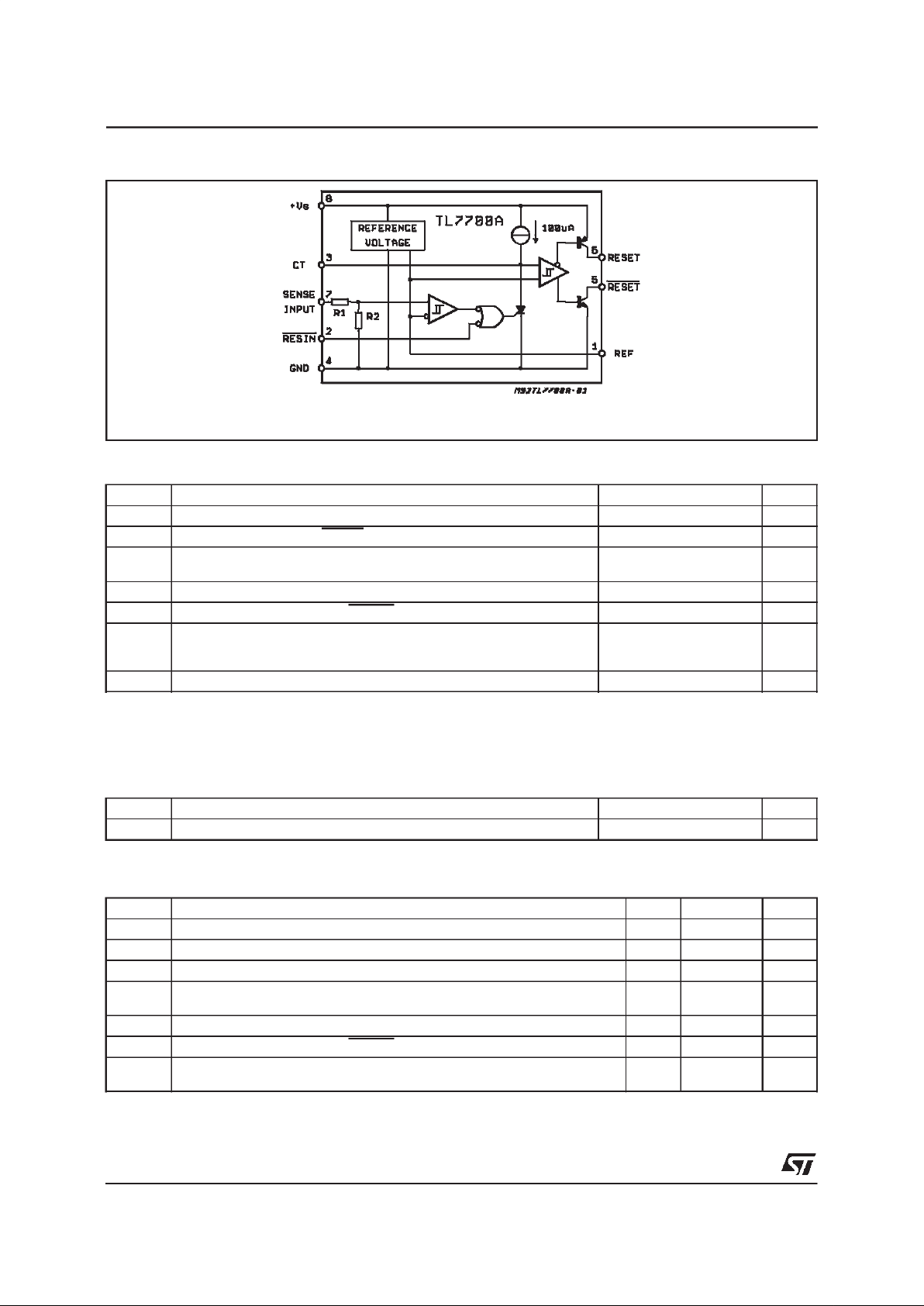
TheTL7700Aseriesaremonolithicintegratedcircuit
supplyvoltagesupervisorsspecificallydesi-gnedfor
use as reset controllers in microcomputerand microprocessorsystems.During power-upthedevice
teststhesupplyvoltageandkeepsthe RESET and
RESEToutputsactive(high and low, respectively)
as long as the supply voltage has not reached its
nominalvoltage value.Taking RESIN low has the
sameeffect.Toensurethatthe microcomputersystemhasreset,theTL7700Atheninitiatesaninternal
timedelaythatdelaysthereturnofthe resetoutputs
totheirinactivestates.Sincethetimedelayformost
microcomputersandmicroprocessorsisintheorder
of several machinecycles, the device internaltime
delayis determinedby an externaltimedelayisdeterminedbyan externalcapacitorconnectedtothe
C
T
input(pin3).
t
d
=1.3x 10⁴xC
T
Where: CTisin farads(F) and tdinseconds (s).In
addition,when the supplyvoltagedrops below the
nominal value, the outputs will be active until the
supplyvoltagereturnstothe nominalvalue.An externalcapacitor(typically0.1µF)mustbeconnected
to the REF output(pin 1) to reducetheinfluenceof
fasttransientsin the supply voltage.
TheTL7700AIseries is characterizedforoperation
from– 25
o
Cto85oC ; theTL7700ACseriesischar-
acterizedfrom 0
o
Cto70oC.
D
SO8
ORDERINGNUMBERS
Temperature Range Minidip S08
0to70
o
C TL77XXACP TL77XXACD
-25to 85
o
C TL77XXAIP TL77XXAID
PIN CONNECTION (top view)
1/7
*
TL7702A R1 =0Ω, R2 = open; TL7705A R1= 7.8KΩ, R2 = 10kΩ;TL7709A R1 = 19.7KΩ,R2 = 10kΩ;
TL7712A R1 = 32.7kΩ, R2 = 10kΩ; TL7715AR1 = 43.4 KΩ, R2 = 10kΩ.
BLOCK DIAGRAM
ABSOLUTE MAXIMUM RATINGS
Symbol Parameter Value Unit
V
S
Supply Voltage, VCC- (see note 1) 20 V
V
i
Input Voltage Range at RESIN -0.3 to 20 V
V
i
Input Voltage at SENSE : TL7702A (see note 2)
TL7705A
-0.3 to 6
-0.3 to 10
V
I
OH
High-level Output Current at RESET -30 mA
I
OL
Low-level Output Current at RESET 30 mA
T
amb
Operating Free-air Temperature Range :
TL77XXAI
TL77XXAC
-25 to 85
0to70
o
C
T
stg
Storage Temperature Range -65 to 150
o
C
Notes: 1. All voltagevaluesare withrespect to the networkground terminal
2. For the TL7700A, thevoltage appliedto the SENSEterminal must neverexceed V
s
.
THERMAL DATA
Symbol Parameter Value Unit
R
th j-amb
Thermal Resistance Junction-ambient Max. 120
o
C/W
RECOMMENDED OPERATING CONDITIONS
Symbol Parameter Min. Max. Unit
V
S
Supply Voltage 3.6 18 V
V
IH
High-level Input Voltage at RESIN 2 V
V
IL
Low-level Input Voltage at RESIN 0.6 V
V
i
Voltage at Sense Input TL7702A
TL7705A
0
0
See note 310V
I
OH
High-level Output Current at RESET -16 mA
I
OL
Low-level Output Current at RESET 16 mA
T
amb
Operating Free-air Temperature Range TL77-AI
TL77-AC
-25
0
85
70
o
C
Note : 3. Forproper operation of theTL7702A,thevoltage applied totheSENSEterminalshould not exceed Vs-1V or6V,whicheverisless.
TL7700A Series
2/7
ELECTRICAL CHARACTERISTICS these specificationsunless otherwisespecified, apply for :
T
amb
= –25 to 85oC (TLXXAI),T
amb
= 0 to 70oC (TL77XXAC)
Symbol Parameter Test Conditions (1) Min. Typ. Max. Unit
V
OH
High-level Output Voltage at RESET IOH= –16mA Vs-
1.5
V
V
OL
Low-Level Output Voltage at RESET IOL= 16mA 0.4 V
V
ref
Reference Voltage T
amb
=25oC 2.48 2.53 2.58 V
V
T
Threshold Voltage at SENSE Input TL7702A
TL7705A
Vs= 3.6V to 18V
T
amb
=25oC
2.48
4.5
2.53
4.55
2.58
4.6
V
V
T
Threshold Voltage at SENSE Inpu TL7702A
TL7705A
Vs= 3.6V to 18V 2.45
4.45
2.53
4.55
2.58
4.6
V
V
T+,VT–
Hysteresis (2) at SENSE Input TL7702A
TL7705A
Vs= 3.6V to 18V
T
amb
=25oC
10
15
mV
I
I
Input Current at RESIN Input Vi= 2.4V to V
S
Vi= 0.4V
20
-100
µ
A
I
I
Input Current at SENSE Input TL7702A V
ref<Vi<Vs
- 1.5V 0.5 2
µ
A
I
OH
High-level Output Current at RESET VO= 18V 50
µ
A
I
OL
Low-level Output Current at RESET VO=0V -50 µA
I
S
Supply Current All Inputs and out.
open
1.8 3.3 mA
Notes:
1. All characteristicsare measured withC = 0.1µF from Pin1 toGND, and withC = 0.1µF fromPin 3 to GND.
2. Hysteresis is thedifferencebetween thepositive going inputthreshold voltage. V
T+
,and thenegativegoing inputthreshold
voltage, V
T-
.
SWITCHING CHARACTERISTICS
Symbol Parameter Test Conditions Min. Typ. Max. Unit
t
pi
Pulse Width at SENSE Input Vih=V
ityp
+0.04 x V
i
ViL=V
ityp
–0.04 x V
i
0.9
µ
s
t
pi
Pulse Width at RESIN Input 0.4
µ
s
t
po
Pulse Width at Output CT= 0.1µF 0.65 1.3 2.6 ms
t
pdHL
Propagation Delay Time from RESIN
to RESET
CL= 100pF, Vs= 5V, RL= 4.7k
Ω
1
µ
s
t
r/f
Rise/Falltime at RESET and RESET CL= 10pF, Vs= 5V, RL= 4.7k
Ω
1
µ
s
TL7700A Series
3/7
 Loading...