

SGS Thomson Microelectronics SERCON410B, SERCOS Datasheet

SERCON410B
DATASHEET

USE IN LIFE SUPPORT DEVICESOR SYSTEMSMUSTBEEXPRESSLYAUTHORIZED.
SGS-THOMSON PRODUCTS ARE NOT AUTHORIZED FOR USE AS CRITICAL COMPONENTS IN LIFE SUPPORT
DEVICES OR SYSTEMS WITHOUT THE EXPRESS WRITTEN APPROVAL OF SGS-THOMSON Microelectronics.
As used herein :
1. Life support devices or systems are those which (a) are
intended for surgical implant into the body,or (b)support
or sustain life, and whose failure to perform, when properly used in accordance with instructions for use provided with the product, can be reasonably expected to
result in significant injury to the user.
2. A critical component is any component of a life support
device or system whose failure to perform can reasonably be expected to cause the failure of the life support
device or system, or to affect its safety or effectiveness.

SERCON410BDATASHEET
INDEX
Page
Number
SERCON410B .................................... 1
1 GENERALDESCRIPTION ............................... 5
2 PIN DESCRIPTION ........................................ 6
3 ELECTRICALCHARACTERISTICS ............................... 9
3.1 ABSOLUTEMAXIMUM RATINGS . . . . . . . . . . . . . . . . . . . . . . . . . . . . . 9
3.2 RECOMMENDEDOPERATING . . . . . . . . . . . . . . . . . . . . . . . . ...... 9
3.3 DC ELECTRICALCHARACTERISTICS . . . . . . . . . . . . . . . . . . . . . . . . . . 9
3.4 AC ELECTRICALCHARACTERISTICS . . . . . . . . . . . . . . . . . . . . . . . . . . 11
3.4.1 ClockInput MCLK . . . . . . . . . . . . . . . . . . . . . . . . . . . . . . . . 11
3.4.2 ClockInput SCLK . . . . . . . . . ........................ 11
3.4.3 SerialClock . . . . . . . . . . . . . . . . . . . . . . . . . . . . . . . . . . . . 12
3.4.4 AddressLatch . . . . . . . . . . . . . . . . . . . . . . . . .......... 12
3.4.5 ReadAccessof Control Registers . . . . . . . . . . . . . . . . . . . . . . . . 13
3.4.6 ReadAccessof Dual Port RAM . . . . . . . . . . . . . . . .......... 14
3.4.7 WriteAccess to Control Registers . . . . . ................... 15
3.4.8 WriteAccess to Dual PortRAM . . . . . . . . . . . . . . . . . . . . . . . . . . 16
4 CONTROLREGISTERSAND RAM DATA STRUCTURES .................... 17
4.1 CONTROL REGISTERADDRESSES . . . . . . . . . . . . . . . . . . . . . . . . . . . 17
4.2 DATA STRUCTURES WITHINTHE RAM . . . . . . . . . . . . . . . . . . . . . . . . . 23
4.2.1 TelegramHeaders . . . . . . . . . . . . . . . . . . . . . . . . . . . . . . . . 23
4.2.2 DataContainers . . . . . . . . . . . . . . . . . . . . . ............ 25
4.2.3 EndMarker . . . . . . . . . . . . . . . . . . . . . . . . . . . . . . . . . . . . 26
4.2.4 ServiceContainers . . . . . . . . . . . . . . . . . . . . . . . . . . . . . . . . 26
5 PACKAGE MECHANICAL DATA ................................. 29
6 ADDITIONALSUPPORTAND TOOLS .............................. 29
6.1 SERCOS INTERFACESPECIFICATION . . . . . . . . . . . . . . . . . . . . . . . . . 29
6.2 SOFTWAREAND BOARDSFOR THE SERCON410B . . . . . . . . . . . . . . . . . . 29

NOTES:
SERCON410B
SERCON410B
PRELIMINARY DATA
This is Preliminary Data from SGS-THOMSON. Detailsare subject tochange without notice.
May 1994
SERCOS INTERFA CECONTROL L E R
(Ordering Number: SERGBQA)
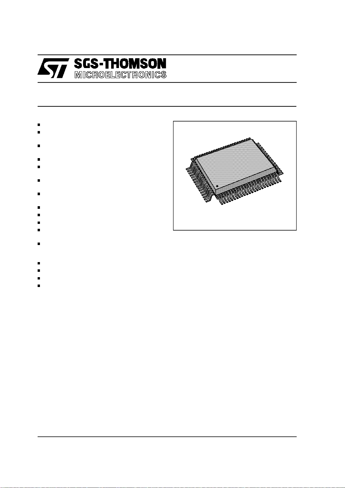
PQFP100
Single-chipcontroller for SERCOS interface
Real timecommunication for industrial control
systems
8/16-bitbus interface, Intel and Motorola con-
trol signals
Dual portRAMwith 1024 words * 16-bit
Data communicationsvia optical fiber rings, RS
485 rings and RS485 busses
Maximumtransmissionrateof 4 Mbaud with in-
ternal clock recovery
Maximumtransmissionrateof 10 Mbaud with
external clockrecovery
Internal repeater for ring connections
Full duplex operation
Modulationof power of optical transmitterdiode
Automatictransmissionof synchronous and
data telegrams in the communicationcycle
Flexible RAM configuration, communication
data stored in RAM (single or double buffer)or
transfervia DMA
Synchronizationby external signal
Timing control signals
Automaticservicechannel transmission
100-pin plasticflat-packcasing
1/30
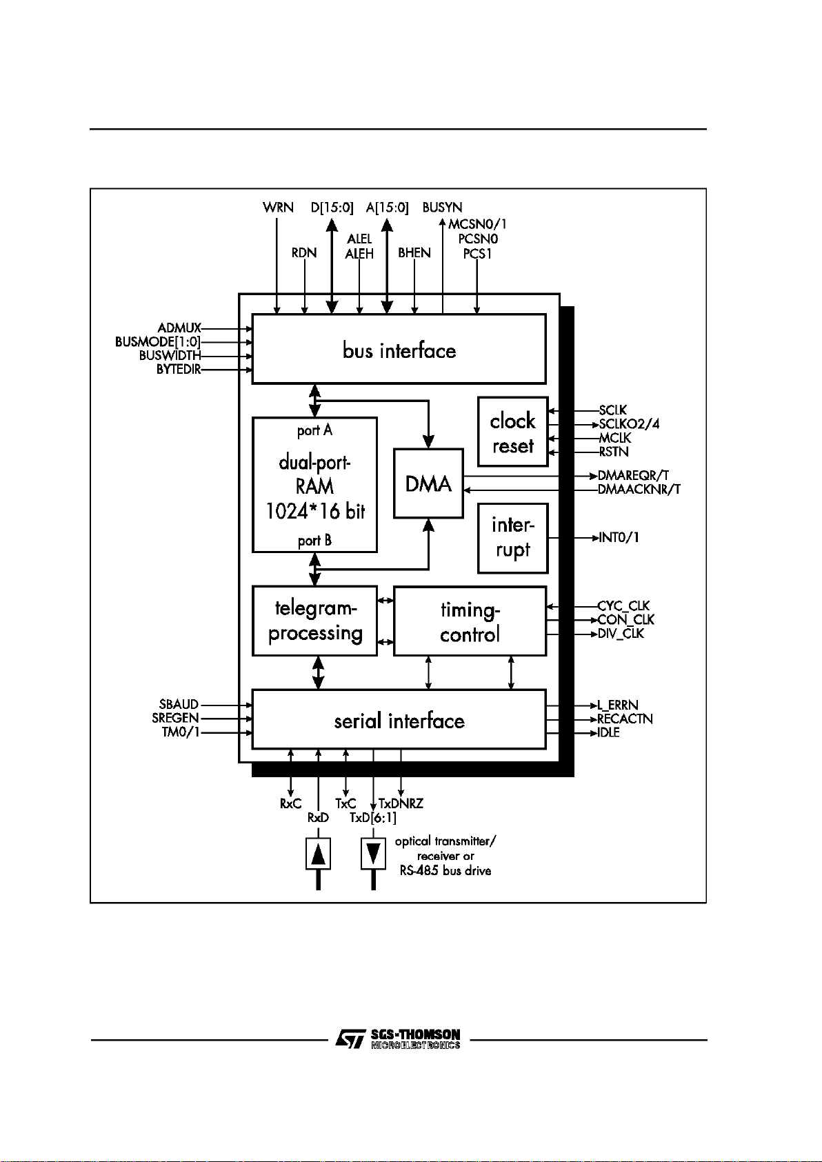
Figure1. SERCON410B Block Diagram
SERCON410B
2/30

Figure2. SERCON410B Pin Configuration
SERCON410B
3/30

Figure3. SERCOS Interface withRing Connection
Figure4. SERCON410B with RS-485 bus Connection
SERCON410B
4/30

1 GENERALDESCRIPTION
The SERCOS interface controller SERCON410B
is anintegrated circuit forSERCOSinterface communication systems. The SERCOS interface is a
digital interface for communication between systems which have to exchange information cyclically at short, fixed intervals (65 µs to 65 ms).It is
appropriate for the synchronous operation of distributed control or test equipment (e.g. connection
between drivesand numeric control).
A SERCOS interfacecommunication system consists of one master and several slaves (Fig. 3).
These units are connected by a fiber optical ring.
This ring startsand ends at the master.The slaves
regenerate and repeat their received data or send
their owntelegrams. By this method the telegrams
sent by the master are received by all slaveswhile
the master receives data telegrams from the
slaves. The optical fiber assures a reliable highspeed datatransmission with excellent noise immunity.
The SERCOS interface controller contains all the
hardware-related functions of the SERCOS interface and considerably reduces thehardware
costs and the computing time requirements of the
microprocessor. It is the direct link between the
electro-opticalreceiver and transmitterand the microprocessorthat executes the control algorithms.
The SERCON410Bcanbeused bothfor SERCOS
interface mastersand slaves.
The circuitcontains the followingfunctions(Fig.1):
-
Interface to the microprocessor with a data
bus width of 8 or 16 bits and with control lines
according to Intel or Motorola standards.
-
A serial interface for making a direct connection with the optical receiver and transmitter of
the fiber optic ring or with drivers to an electric
ring or bus. Data and clock regeneration, the
repeater for ring topologies and the serial
transmitter and receiver are integrated. The
signals are monitored and test signals generated. The serial interface operates up to
4Mbaud without external circuitry and up to 10
Mbaud with external clock regeneration.
-
A dual port RAM (1024 * 16 bit) for control and
communication data. The organization of the
memoryis flexible.
-
Telegram processing for automatic transmission and monitoring of synchronous and data
telegrams. Only transmission data which is intended for the particular interface user is processed. The transmitted data is either stored in
the internal RAM (single or double buffer) or
transferred via direct memory access (DMA).
The transmission of service channel information over several communication cycles is executed automatically.
In addition to the SERCOS interface the SERCON410B can also be used for other real-time
communications tasks. As an alternative to the fiberoptical ring also bus topologies with RS-485
signals are supported (Fig. 4). The SERCON410B
is therefore suitable for a wide range of applications.
SERCON410B
5/30

2 PIN DESCRIPTION
Signal (s) Pin (s) IO Function
D15-0
77-80,
82-85,
87-90,
92-95
I/O
Data bus:for 8-bit-widebus interfaces, data is writtento and read via D7-0,
for 16-bit-wide bus interfaces via D15-0. When ADMUX is 1, the address
which is storedin the address latchwith ALEL and ALEH isinput via D15-0.
A15-0
56-59,
61-64,
66-69,
71-74
I/O
Addressbus: when ADMUX is 0the pins are inputs, when ADMUXis 1, they
are outputsfor the addressstored with ALEL (A7-0)and ALEH(A15-8). In
the 8-bit bus mode, A0 distinguishes which byte is transmitted via
D7-0 (depends on BYTEDIR). In the 16-bit bus mode, data is tansferred via
D7-0 only when A0 is 0. A10-1 selects the words of the internal RAM; A61the controlregisters.
ALEL, ALEH 54, 53 I
Address latchenable, low and high, active high: they are only used when
ADMUX is 1. When ALEL/ALEH is 1, the signals go from the data bus to
the address bus, when ALEL/ALEH = 0, they store the address. When
ADMUX is 0, ALEL/ALEH have to be connected to V
DD
.
RDN 51 I
Read: for the Intel bus interface, data is read when RDN is 0. For the
Motorola bus interface, data is read or written to when RDN is 0
(BUSMODE1 = 0) or RDN is 1 (BUSMODE1 = 1).
WRN 52 I
Write: for the Intel bus interface, data is written to when WRN is 0. For the
Motorola bus interface, WRN selects read (WRN = 1) and write (WRN = 0)
operations of the data bus.
BHEN 75 I
Byte high enable, active low: in the 16-bit bus mode, data is transferred via
D15-8 when BHEN is 0.
MCSN0,
MCSN1
46,47 I
Memory chip select, active low: to access theinternal RAM MCSN0 and
MCSN1 must be 0.
PCSN0,
PCS1
48,49 I
Periphery chip select, active low (PCSN0) and active high (PCSN1): to
access the control registers PCSN0 must equal 0 and PCS1 must equal 1.
BUSYN 45 O
RAM busy, active low: becomes active if an access to an address of the
dual port RAM is performed simultaneously to an access to the same
memory location by the internal telegram processing.
DMAREQR 38 O
DMA request receive, active high: becomes active ifdata from the receive
FIFO can be read. At the beginning of the read operation of the last word of
the receive FIFO, DMAREQR becomes inactive.
DMAACKRN 40 I
DMA acknowledge receive, active low: when DMAACKRN is 0, the receive
FIFO is read, independent of the levels on A6-1 and the chip select signals.
DMAREQT 39 O
DMA request transmit, active high: becomes active when data can be
written to the transmit FIFO. DMAREQT becomes inactive again at the
beginning of the last write access to the transmit FIFO.
DMAREQTN 41 I
DMA acknowledge transmit, active low: when DMAACKTN is 0, the
transmit FIFO is written to when there isa bus writeaccess independent of
the levels on A6-1 and the chip select signals.
ADMUX 96 I
Address databus: when ADMUX is 0 A15-0 are the address inputs, when
ADMUX is 1 A15-0 are theoutputs ofthe address latch.
BUSMODE0,
BUSMODE1
97,98 I
Busmode: BUSMODE0= 0 turnson theIntelbusinterface(RDN= read,
WRN= write),BUSMODE0= 1 selects theMotorola interface (RDN= data
strobe, WRN= read/write). BUSMODE1selects the 0-activedata strobe
(BUSMODE1 = 0)or the1-activedata strobe(BUSMODE1= 1).
BUSWIDTH 99 I Buswidth:selectsthe 8-bit- (0)or the16-bit-wide interface(1).
Table 1. SERCON410B I/O Port FunctionSummary
SERCON410B
6/30

PIN DESCRIPTION(Continued)
Signal (s) Pin (s) IO Function
BYTEDIR 100 I
Byte address sequence: when BYTEDIR is0, A0 = 0 addresses the lower
8 bits of a word (low byte first), when BYTEDIR is 1, the upper 8 bits of a
word are addressed (high byte first).
INT0, INT1 44,43 O
Interrupts, active low or active high. Interrupt sources and signal polarity
are programmable.
SREGEN 28 I
Internal regeneration. When SREGEN is 0, clock and data regeneration
are turnedoff. RxC and TxC are clock inputs. WhenSREGEN is 1, clock
and data regeneration are turned on. RxC and TxC output the internally
generated clocks.
SBAUD 29 I
Baud rate. When regeneration is turned on, SBAUD selects the baud rate
(f
SCLK/
16 whenSBAUD is 0, f
SCLK
/32 when SBAUD is 1). Can be
overwritten by the microprocessor.
RxD
14
I Receive data for the serial interface.
RxC
12
I/O
Receive clockfor the serialinterface. When regeneration is turned off
(SREGEN = 0), clock input for the serial receiver and transmitter (only
when repeater is turned on); when regeneration is turned on (SREGEN= 1)
output ofthe internally generated receive clock. Themaximum frequency
is 10 MHz.
RECACTN
26
O
Receive active,active low. Indicates that the serial receiver is receiving a
telegram.
TxD1
16
O Transmit data. The pin can be switched to a high impedance state.
TxD6-2
22,21,2
0,
18,17
O
Transmit data or output port. The pins either output the serial data or can
be used as parallel output ports. When they output transmit data, each pin
can be switched to a high impedance state individually.
TxDNRZ
24
O NRZ-coded transmit data.
TxC
13
I/O
Transmit clock for the serial interface. When regeneration is turned off
(SREGEN = 0) and the repeater is turned off,it is the clock input for the
serial transmitter; when regeneration is turned on (SREGEN = 1) itis the
output forthe internally generated transmit clock. The maximum frequency
is 10 MHz.
IDLE
25
O Transmitter active, active low. When transmitting own data IDLE is 0.
TM0, TM1
30,31
I
Turn on test generator: TM0 = 0 switches TxD1-6 to continuous signal light,
TM1 = 0 switch-over to zero bit stream. The processor can overwrite the
level of TM1-0.
L_ERRN
32
O
Line error, active low: goes low when signal distortion is too high or when
the receive signal is missing. The operating mode is programmed by the
processor.
CYC_CLK
34
I
SERCOS interface cycle clock: CYC_CLK synchronizes the
communication cycles.The polarity is programmable.
CON_CLK
35
O
Control clock: becomes active within a communication cycle. Time,
polarity and width are programmable.
DIV_CLK 36 O
Divided control clock: becomes active several times within a ommunication
cycle. Number of pulses, start time, repetition rate and polarity are
programmable, the pulse width is 1µs.
SCLK 2 I
Serial clock for clock regeneration: the frequency is 16 or 32 times the
baud rate, the maximum frequency is 64 MHz.
Table 1. SERCON410B I/O Port FunctionSummary
(Continued)
SERCON410B
7/30
 Loading...