

T
SERCOS INTERFACE CONTROLLER
■ Single-chip controller for SERCOS interface
■ Real time communication for in dustrial control
systems
■ 8/16-bit bus interface, Intel and Motorola control
signals
■ Dual port RAM with 2048 word *16-bit
■ Data communications via optical fiber rings, RS
485 rings and RS 485 busses
■ Maximum transmission rate of 16 Mbaud with
internal clock recovery
■ Internal repeater for ring connections
■ Full duplex operation
■ Modulation of power of optical transmitter diode
■ Automatic transmission of synchronous and
data telegrams in the communication cycle
■ Flexible RAM configuration, communication
data stored in RAM (s ingle or doubl e buffer) or
transfer via DMA
■ Synchronization by external signal
SERCON816
PQFP100
ORDERING NUMBERS: SERC816
SERC816/TR
■ Timing control signals
■ Automatic service channel transmission
■ Watchdog to monitor software and external
synchronization signals
■ Compatible mode to SERCON410B SERCOS
interface controller
■ 100-pin plastic flat-pack casing
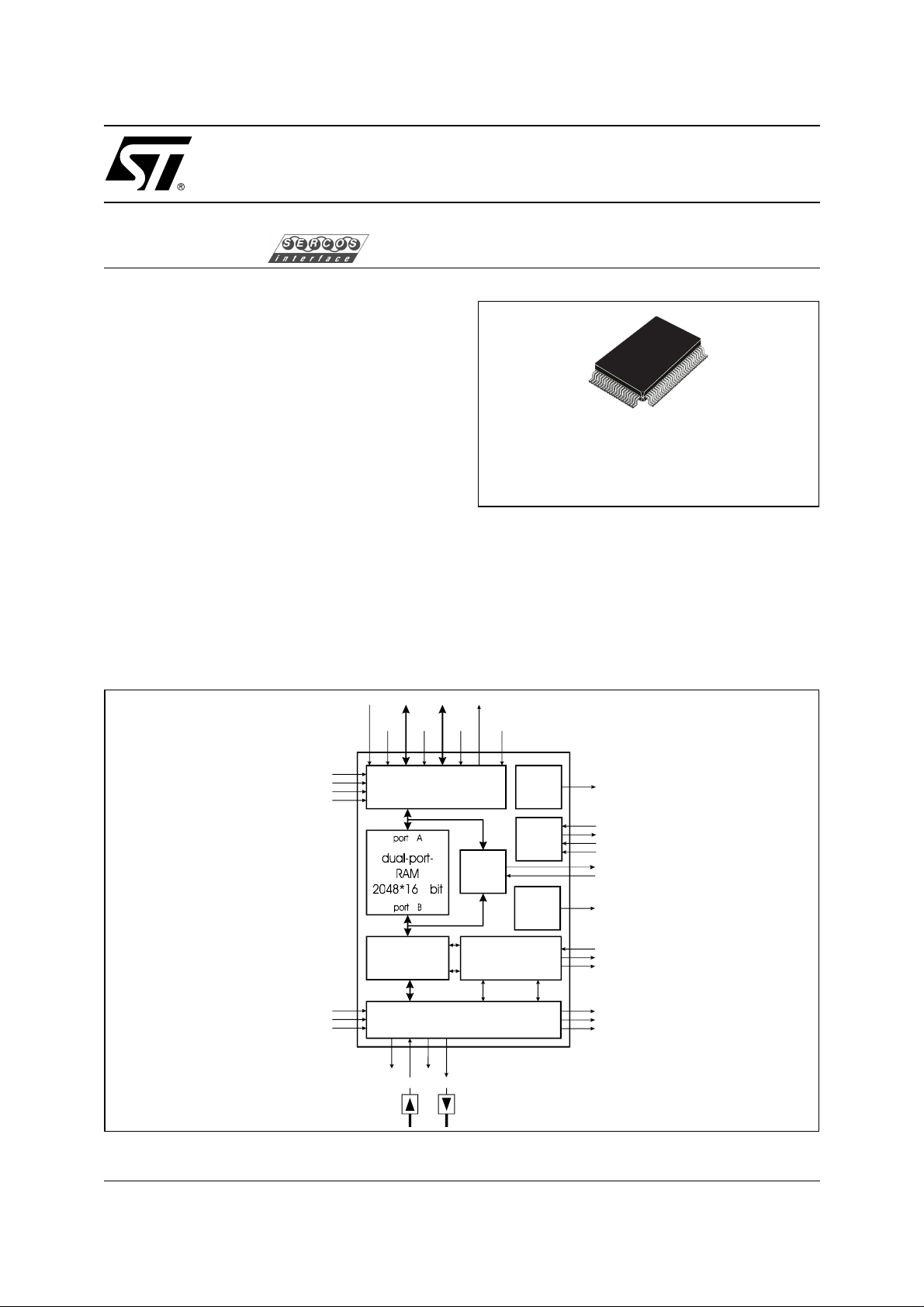
Figure 1. SERCON816 Block Diagram
WRN D[15:0] A[15:0] BUSYN
ADMUX
BUSMO DE[ 1 : 0 ]
BUSWIDTH
BYTEDIR
SBAUD
SBAUD 1 6
TM0/1
ALE L
RDN
ALE H
bus interface
telegram-
processing
serial interface
RxC
TxC
RxD
TxD[6:1]
MCSN0/1
PC SN 0
BHEN
PCS1
DMA
timingcontrol
optical transmitter/
receiver or
RS-485 bus drive
inter-
rup t
clock
reset
watch-
dog
INT 0/1
SCLK
SCLKO 2 / 4
MCLK
RSTN
DMAR EQR/T
DMAACKNR/
WDOGN
CYC_CLK
CON_CLK
DIV_CLK
L_ERRN
REC A C TN
IDLE
January 2003
1/23

SERCON816
TABLE OF CONTENTS
1 GENERAL DESCRIPTION.................................................................................................................3
2 Pin Description................................................................................................................................... 5
3 Electrical (DC and AC) Characteristics..............................................................................................7
3.1 Absolute Maximum Ratings .....................................................................................................7
3.2 Recommended Operating Conditions......................................................................................8
3.3 ELECTRICAL CHARACTERISTCS ........................................................................................ 8
3.4 Power Dissipation....................................................................................................................9
3.4.1 Power Dissipation Considerations....................................................................................9
3.5 AC Electrical Characteristics..................................................................................................10
3.5.1 Clock Input MCLK...........................................................................................................10
3.5.2 Clock Input SCLK...........................................................................................................11
3.5.3 Address Latch... .............. ....... .............. .............. ............... ....... .............. .............. ....... ....11
3.5.4 Read Acce ss of Control Registers.................................................................................. 12
3.5.5 Read Access of Dual Port RAM .............................................................. ..... ....... ....... ....13
3.5.6 Write Access to Control Registers..................................................................................14
3.5.7 Write Access to DUAL Port RAM...................................................................................15
4 Control Registers and RAM Data Structures....................................................................................16
4.1 Control Register Addresses...................................................................................................16
4.2 Data Structures within the RAM.............................................................................................16
4.2.1 Telegram Headers.............................................................. ....... .. .......... ....... .. .......... ......16
4.2.2 Data Containe r s.............. ....... .............. .............. ............... ....... .............. .............. ........ ...17
4.2.3 End Marker.....................................................................................................................18
4.2.4 Service Conta ine r s......... .............. ....... .............. ............... .............. ....... .............. ...........18
5 Additional Specifications, Tools and Suppo rt...................................................................................21
5.1 Additional Spec ifications ........................................................................................................21
5.2 Hardware and Software Components.................................................................. ....... ....... ....21
5.3 Tools........................................... ........................................................... ................... .............21
6 Package Mechanical Data:
SERCON816 100 Pin Plastic Quad Flat Pack Package (PQFP100) ........................................... ....22
2/23
SERCON816
1 GENERAL DESCRIPTION
The SERCOS interface controller SERCON816 is an integrated circuit for SERCOS interface communication
systems. The SERCOS interface is a digital interface for communication between systems which have to exchange information cyclically at short, fixed intervals (62,5 s to 65 ms). It is appropriate for the synchronous
operation of distributed control or test equipment (e.g. connection between drives and numeric control).
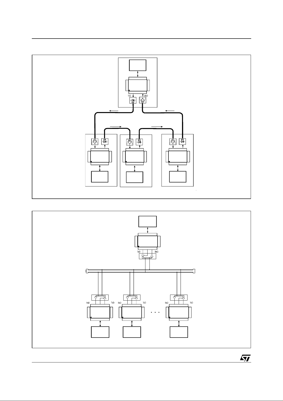
A SERCOS interface communication system consists of one master and several slaves. These units are
connect ed by a fiber optical ring. This ring starts and ends at the maste r. T he slaves regenerate and repeat
their received data or send their own telegrams. By this method the telegrams sent by the master are received by all slaves while the master receives data telegrams from the slaves. The optical fiber assures a
reliabl e hi gh-speed dat a t ransmissio n wi t h excellent noi s e i m m unity.
The SERC O S i nt erf ace contro l le r c ontains al l the hardware-relat ed f unctions of the SERCOS in te rface and
considerably reduces the hardware costs and the computing time requirements of the microprocessor. It is
the dire ct link betw een th e elect ro-op tical rece iver an d tran smit ter a nd the micr oproc essor that exec utes th e
control algorithms. The SERCON816 can be used bo th for SERCOS interface masters and slaves.
The circuit contains the following functions (Fig. 1):
– Interface to the microprocessor with a data bus width of 8 or 16 bits and with control lines according to
Intel or Motorola standards.
– A serial interface for making a direct c onnection with the opti cal rec eiver and tr ansmitter of the fi ber optic r ing
or with drivers to an elec tric ring or bus. Data and cl ock r egeneratio n, the repeater for ring to pologies and the
serial transmitter and receiver are integrated. The signals are monitored and test signals generated. The serial interface operates up to 16 Mbaud without external circuitry.
– A dual port RAM (2048 * 16 bi t) for control and communication data. The organization of the memory is flexible.
– Telegram processing for automatic transmission and monitoring of synchronous and data telegrams. Only
transmission data which is intended for the particular interface user is processed. The transmitted data is either stored in the internal RAM (single or double buffer) or transferred via direct memory access (DMA). The
transmission of service channel information over several communication cycles is executed automatically.
In addition to the SERCOS interface the SERCON816 c an also be used for other real-time communications tasks. As an alternative to t he fiber optical ring also bus topologies with RS-485 signals are supported
(Fig. 4). The SERCON816 is therefore suitable for a wide range of applications.
Remark: The SERCON816 is based on the former SERCON410B SERCOS interface controller.
Figure 2. SERCON816 Pin Configuration
80 D12
D13
D14
D15
75 BHEN
A0
VDD
VSS 81
D11
D10
D9
D8 85
VDD
D7
D6
D5
D4 90
VSS
D3
D2
D1
D0 95
ADMUX
BUSMODE0
BUSMODE1
BUSWIDTH
BYTDIR 100
VDD 1
SCLK
VSS
MCLK
TEST
SCLK04 5
SCLK02
A5
A7
A8
A9
A4
A1
A2
A6
A3
70 VSS
A10
65 VDD
SERCON816
VSS 15
TxD2
TxD3
RxC
VDD
NDTRO
RxD
OUTZ
TxC
RSTN 10
VDD
TxD1
A11
A12
A13
A14
60 VSS
TxD4 20
TxD5
TxD6
VSS
WRN
ALEH
A15
WDOGN
51 RDN
55 VDD
ALEL
50 VSS
PCS1
PCSN0
MCSN1
MCSN0
45 BUSYN
INT0
INT1
VSS
DMAACKTN
40 DMAACKRN
DMAREQT
DMAREQR
VDD
DIV_CLK
35 CON_CLK
CYC_CLK
VSS
L_ERRN
31 TM1
TM0 30
IDLE 25
VDD
RECACTN
SBAUD
SBAUD16
3/23
SERCON816
Figure 3. SERCON816 with Ring Connection (SERCOS interface)
µP
bus interface
SERC O N 8 1 6
master
fibre optical ring
TxDRxD
bus interface
µP
TxDRxD
bus interface
µP
slave 1 slave 2
Figure 4. SERCON816 with RS-485 bus connection
µP
bus interface
SERC ON8 1 6
IDLE
master
SERC O N 8 1 6SERCON816SERC O N 8 1 6
bus interface
µP
TxDRxD
sla ve n
4/23
IDLE IDLE IDLE
SERC ON8 1 6 SERC ON8 1 6 SERCON816
businterface businterface businterface
µP µP µP
sla ve 1 slave 2
SERCRING.CDR
slave n
SERCON816
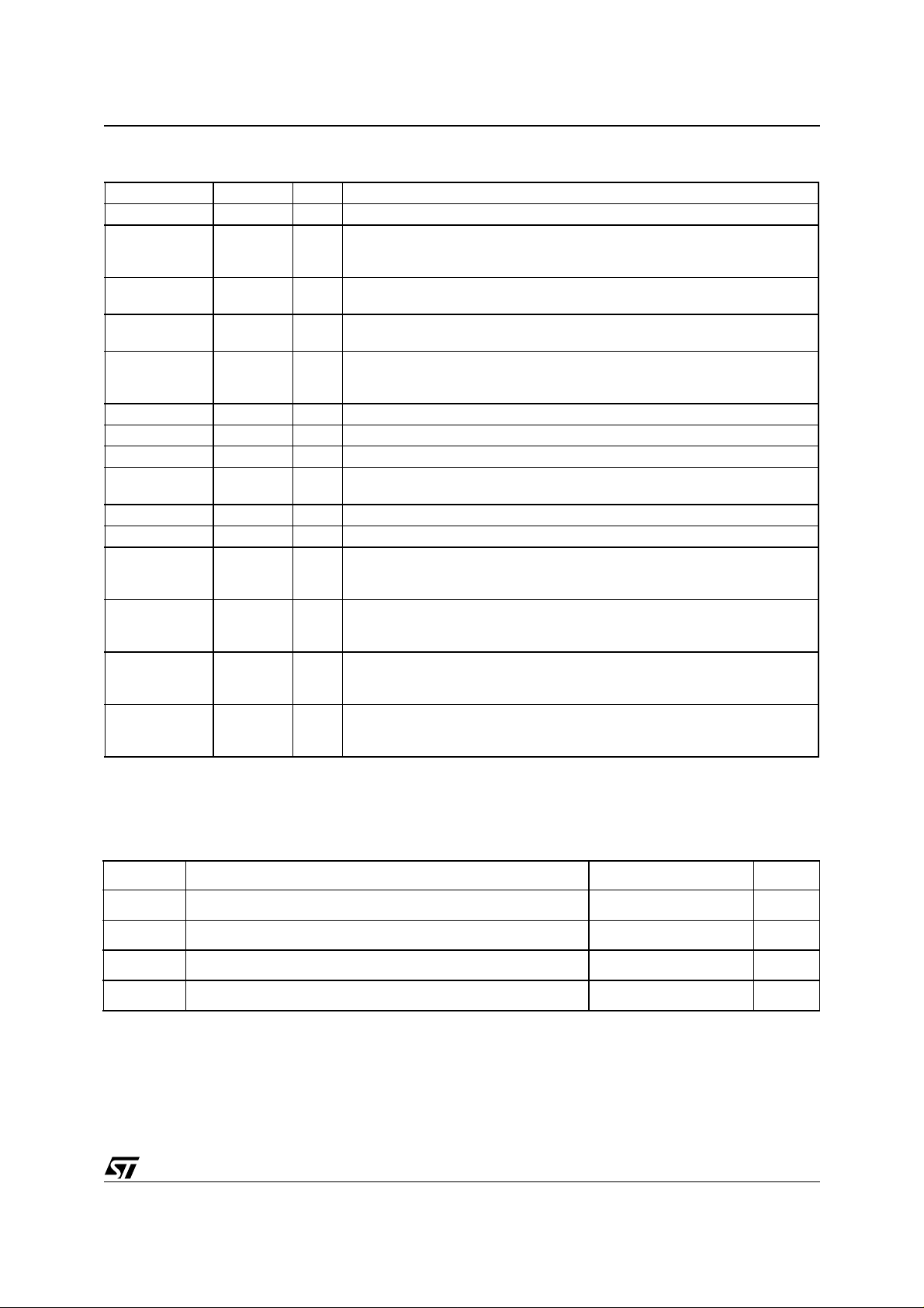
2 PIN DESCRIPTION
Table 1. S E R CON816 I/O Port Func tion Su m m ary
Signal(s) Pin(s) IO Function
D15-0 77-80,
ALEL, ALEH 54, 53 I Address latch enable, low and high, active high: they are only used when
RDN 51 I Read: for the Intel bus interface, data is read when RDN is 0. For the Motorola
WRN 52 I Write: for the Intel bus interface, data is written to when WRN is 0. For the
BHEN 75 I Byte high enable, active low: in the 16-bit bus mode, data is transferred via
MCSN0,
MCSN1
PCSN0,
PCS1
BUSYN 45 O RAM busy, active low: becomes active if an access to an address of the dual
DMAREQR 38 O DMA request receive, active high: becomes active if data from the receive
DMAACKRN 40 I DMA acknowledge receive, active low: when DMAACKRN is 0, the receive
DMAREQT 39 O DMA request transmit, active high: becomes active when data can be written
DMAACKTN 41 I DMA acknowledge transmit, active low: when DMAACKTN is 0, the transmit
ADMUX 96 I Address data bus: when ADMUX is 0 A15-0 are the address inputs, when
BUSMODE0,
BUSMODE1
BUSWIDTH 99 I Bus width: selects the 8-bit- (0) or the 16-bit-wide interface (1).
BYTEDIR 100 I Byte address sequence: when BYTEDIR is 0, A0 = 0 addresses the lower 8
INT0, INT1 44,43 O Interrupts, active low or active high. Interrupt sources and signal polarity are
SBAUD16 28 I Baud rate and SERCON410B compatible mode: SBAUD and SBAUD16
SBAUD 29 I Baud rate. Can be overwritten by the microprocessor.
82-85,
87-90,
92-95
46,47 I Memory chip select, active low: to access the internal RAM MCSN0 and
48,49 I Periphery chip select, active low (PCSN0) and active high (PCS1): to access
97,98 I Bus mode: BUSMODE0 = 0 turns on the Intel bus interface (RDN = read,
I/O
Data bus: for 8-bit-wide bus interfaces, data is wri
16-bit-wide bus interfaces via D15-0. When ADMUX is 1, the address which is
stored in the address latch with ALEL and ALEH is input via D15-0.
ADMUX is 1. When ALEL/ALEH is 1, the signals go from the data bus to the
address bus, when ALEL/ALEH = 0, they store the address. When ADMUX is
0, ALEL/ALEH have to be connected to VDD.
bus interface, data is read or written to when RDN is 0 (BUSMODE1 = 0) or
RDN is 1 (BUSMODE1 = 1).
Motorola bus interace, WRN selects read (WRN = 1) and write (WRN = 0)
operations of the data bus.
D15-8 when BHEN is 0.
MCSN1 must be 0.
the control registers PCSN0 must equal 0 and PCS1 must equal 1.
port RAM is performed simultaneously to an access to the same memory
location by the internal telegram processing.
FIFO can be read. At the beginning of the read operation of the last word of
the receive FIFO, DMAREQR becomes inactive.
FIFO is read, independent of the levels on A6-1 and the chip select signals.
to the transmit FIFO. DMAREQT becomes inactive again at the beginning of
the last write access to the transmit FIFO.
FIFO is written to when there is a bus write access independent of the levels
on A6-1 and the chip select signals.
ADMUX is 1 A15-0 are the outputs of the address latch.
WRN = write), BUSMODE0 = 1 selects the Motorola interface (RDN = data
strobe, WRN = read/write). BUSMODE1 selects the 0-active data strobe
(BUSMODE1 = 0) or the 1-active data strobe (BUSMODE1 = 1).
bits of a word (low byte first), when BYTEDIR is 1, the upper 8 bits of a word
are addressed (high byte first).
programmable.
selects the baud rate for the serial interface. If SBAUD16 is ‘1’ the
SERCON410B compatible mode is selected.
tten to and read via D7-0, for
5/23

SERCON816
Table 1. S E R CON816 I/O Port Func tion Su m m ary (continued)
Signal(s) Pin(s) IO Function
RxD 14 I Receive data for the serial interface.
RxC 12 O Receive clock for the serial interface. Output of the internally generated
RECACTN 26 O Receive active, active low. Indicates that the serial receiver is receiving a
TxD1 16 O Transmit data. The pin can be switched to a high impedance state.
TxD6-2 22,21,20,
18,17
TxC 13 O Transmit clock for the serial interface. Output for the internally generated
IDLE 25 O Transmitter active, active low. When transmitting own data IDLE is 0.
DMAREQT 39 O DMA request transmit, active high: becomes active when data can be written
DMAACKTN 41 I DMA acknowledge transmit, active low: when DMAACKTN is 0, the transmit
ADMUX 96 I Address data bus: when ADMUX is 0 A15-0 are the address inputs, when
BUSMODE0,
BUSMODE1
BUSWIDTH 99 I Bus width: selects the 8-bit- (0) or the 16-bit-wide interface (1).
BYTEDIR 100 I Byte address sequence: when BYTEDIR is 0, A0 = 0 addresses the lower 8
INT0, INT1 44,43 O Interrupts, active low or active high. Interrupt sources and signal polarity are
SBAUD16 28 I Baud rate and SERCON410B compatible mode: SBAUD and SBAUD16
SBAUD 29 I Baud rate. Can be overwritten by the microprocessor.
RxD 14 I Receive data for the serial interface.
RxC 12 O Receive clock for the serial interface. Output of the internally generated
RECACTN 26 O Receive active, active low. Indicates that the serial receiver is receiving a
TxD1 16 O Transmit data. The pin can be switched to a high impedance state.
TxD6-2 22,21,20,
TxC 13 O Transmit clock for the serial interface. Output for the internally generated
IDLE 25 O Transmitter active, active low. When transmitting own data IDLE is 0.
TM0, TM1 30,31 I Turn on test generator: TM0 = 0 switches TxD1-6 to contiuous signal light,
97,98 I Bus mode: BUSMODE0 = 0 turns on the Intel bus interface (RDN = read,
18,17
receive clock.
telegram.
O Transmit data or output port. The pins either output the serial data or can be
used as parallel output ports. When they output transmit data, each pin can be
switched to a high impedance state individually.
transmit clock.
to the transmit FIFO. DMAREQT becomes inactive again at the beginning of
the last write access to the transmit FIFO.
FIFO is written to when there is a bus write access independent of the levels
on A6-1 and the chip select signals.
ADMUX is 1 A15-0 are the outputs of the address latch.
WRN = write), BUSMODE0 = 1 selects the Motorola interface (RDN = data
strobe, WRN = read/write). BUSMODE1 selects the 0-active data strobe
(BUSMODE1 = 0) or the 1-active data strobe (BUSMODE1 = 1).
bits of a word (low byte first), when BYTEDIR is 1, the upper 8 bits of a word
are addressed (high byte first).
programmable.
selects the baud rate for the serial interface. If SBAUD16 is ‘1’ the
SERCON410B compatible mode is selected.
receive clock.
telegram.
O Transmit data or output port. The pins either output the serial data or can be
used as parallel output ports. When they output transmit data, each pin can be
switched to a high impedance state individually.
transmit clock.
TM1 = 0 switch-over to zero bit stream. The processor can overwrite the level
of TM1-0. Select repeater mode at reset time: TM1=0 and TM2=0 repeater
off, all other repeater on.
6/23
SERCON816
Table 1. S E R CON816 I/O Port Func tion Su m m ary (continued)
Signal(s) Pin(s) IO Function
WDOGN 24 O Watchdog output (active low)
L_ERRN 32 O Line error, active low: goes low when signal distortion is too high or when the
CYC_CLK 34 I SER COS interface cycle clock: CYC_CLK synch ronizes the commun ication
CON_CLK 35 O Control clock: becomes active within a communication cycle. Time, polarity
DIV_CLK 36 O Divided control clock: becomes active several times within a communication
SCLK 2 I Serial clock for clock regeneration: the maximum frequency is 64 MHz.
SCLKO2 6 O Clock output: outputs the SCLK clock divided by 2 or 1.
SCLKO4 5 O Clock output: outputs the SCLK clock divided by 4 or 2.
MCLK 4 I Master clock for telegram processing and timing control, frequency 12 to 64
RSTN 10 I Reset, active low. Must be zero for at least 50 ns after power on.
TEST 7 I Test, active high. Has to be tied to VSS.
OUTZ 11 I Puts outputs into high impedance state, active high: OUTZ is 1 puts all pins
NDTRO 9 O NAND tree output. For the test at the semiconductor manufacturers and for
VSS 3,15,23,33
,42,50,60,
70,81,91
VDD 1,8,19,27,
37,55,65,
76,86
receive signal is missing. The operating mode is programmed by the
processor.
cycles. The polarity is programmable.
and width are programmable.
cycle or once in several communication cycles. Number of pulses, start time,
repetition rate and polarity are programmable, the pulse width is 1 µs.
MHz.
into a high impedance state. The clocks are turned off and the circuit is reset.
For the in-circuit test and for turning on the power-down mode.
the connection test after board production. NDTRO is not set to a high
impedance state.
Ground pins:
Power supply +5 V ± 5%.
3 ELECTRICAL (DC AND AC) CHARACTERISTICS
3.1 Absolute Maximum Ratings
Symbol Parameter Value Unit
Supply voltage -0.5 to 6.5 V
Input voltage -0.5 to VDD + 0.5 V
I
Output voltage -0.5 to VDD + 0.5 V
Storage temperature -55 to +150 °C
T
V
V
STG
DD
V
O
7/23

SERCON816
3.2 Recommended Oper ating Conditions
Symbol Parameter Min. Max . Unit
T
A
T
V
DD
f
SCLK
f
MCLK
Notes: 1. Only if PLL is used (SBAUD16=0)
2. For normal operation, dur i ng testing f
Operating temperature -40 85 °C
Chip junction temperature -40 125 °C
J
Operating supply voltage 4.75 5.25 V
Clock frequency SCLK
Clock frequency MCLK
= 0 is possible
MCLK
32
12
1
2
64 MHz
64 MHz
3.3 ELECTRICAL CHARACTERISTCS
(V
= 5V ± 5% T
DD
Symbol Parameter Test Condition Min. Typ. Max. Unit
V
Low level input voltage (TTL)
IL
All inputs
V
High level input voltage (TTL)
IH
All inputs
V
Schmitt trigger hysteresis
hyst
L_ERRN, TXD6-1, MCLK, SCLK,
RSTN, ADMUX, BUSMODE1-0,
BUSWIDTH, BYTEDIR, TM1-0,
SBAUD16, SBAUD, TEST , OUTZ,
RXD, CYC_CLK
= -40 °C to +85 °C, unless otherwise specified)
amb
0.8 V
2.0 V
0.4 0.7 V
Low level input current with pull-
I
IL
up
D15-0, A15-0, TXD6-1, ADMUX,
BUSMODE1-0, BYTEDIR, TM10, SBAUD16, SBAUD, TEST,
OUTZ, RXD, CYC_CLK, BHEN,
MCSN1-0, PCSN0, PCS1,
DMAACKTN, DMAACKRN
High level input current with pull-
I
IH
down
MCLK, SCLK, RSTN, ALEH,
ALEL
Rup Equivalent pull-up resistance V
Rdn Equivalent pull-down resistance VI = V
V
Low level output voltage, all O-
OL
and I/O-pins except TXD6-1,
L_ERRN
V
High level output voltage, all O-
OH
and I/O-pins except TXD6-1,
L_ERRN
8/23
V
V
= V
I
= V
I
= V
I
SS
DD
SS
DD
-40 -100 -240 µA
40 100 240 µA
23 50 112.5 KOhm
23 50 112.5 KOhm
IOI = -4 mA 0.4 V
IOH = +4 mA 2.4 V

SERCON816
3.3 ELECTRICAL CHARACTERISTCS (continued)
(V
= 5V ± 5% T
DD
Symbol Parameter Test Condition Min. Typ. Max. Unit
= -40 °C to +85 °C, unless otherwise specified)
amb
V
V
V
I
C
I
KLU
Low level output voltage, pins
OL
TXD6-1, L_ERRN
High level output voltage, pins
OH
TXD6-1, L_ERRN
Tri-state output leakage VO = 0 V or V
OZ
I/O latch-up current V<VSS V>V
Electrostatic protection Leakage < 1 µA, human body
ESD
Pin capacitance 10 pF
PIN
IOI = -8 mA 0.4 V
IOH = +8 mA 2.4
DD
DD
model
200 mA
2000 V
1 µA
3.4 Power Dissipation
(V
= 5V ± 5% T
DD
Symbol Parameter Test Condition Min. Typ. Max. Unit
P
P
Notes: 1. estimated
Power dissipation 16 Mbaud, MCLK=64 MHz
D
Maximum allowed power
DA
dissipation
= -40 °C to +85 °C, unless otherwise specified)
amb
TA=+85°, no air flow 1000 mW
850
1
mW
3.4.1 Power Dissipation Considerations
Most of the current consumed by CMOS devices is alternate current (AC) which is charging and discharging the capacitances of the pins and internal nodes. The current consum ption ris es with the frequency at
which the pins and internal nodes will toggle and with the capacitances connected to the pins of the device:
P = f · C · V2 (C=capacitance, V=voltage, f=frequency)
For applications which require low power consumption or exceeds the maximum allowed power consumption the following is required:
– Connect unused pins to pull-up or pull-down resistors
– Minimize the capacitive load on the pins
– Reduce clock frequency of SCLK and M CLK
– Minimize accesses to the internal RAM and control registers
The maximum allowed power cons um pt ion is limited by the m ax imum all owed c hi p junction temperature
and by the number of VCC/VDD pins. The chip junction temperature is influenced by the ambient temperature and the package t herm al resistance. T he am bie nt temperature c ou ld be influenced by the ap plication through a good temperature management like heat sinks or ambient air cooling.
9/23

SERCON816
Typical current consumption: measured at 5V (VCC/VDD) and 25°C
f
Mode
410B 64 32 30
816 64 32 80
(MHz) f
SCLK
MCLK
(MHz)
3.5 AC Electrical Characteristics
= 50 pF, VDD = 5 V ± 5% T
(C
load
= -40 °C to +85 °C)
amb
3.5.1 Clock Input MCLK
Figure 5. Tim in g of c l ock M C LK and related outputs
1/f
MCL K
MCLK
t
DMAREQR/T
MCLD
CON_CLK,
DIV _CLK
t
MCLK0
Current (mA)
t
MCLK1
Symbol Parameter Min. Typ. Max. Unit
f
MCLK
t
MCLK0
t
MCLK1
t
MCLD
f
MCLK
f
MCLK
Clock frequency MCLK 12 64 MHz
MCLK low 6 ns
MCLK high 6 ns
Output delay rising edge MCLK to DMAREQR/T, CON_CLK,
DIV_CLK
Baudrate 2 Mbit/s 12 64 MHz
Baudrate 4 Mbit/s 12 64 MHz
20 ns
10/23

SERCON816
3.5.2 Clock Input SCLK
Figure 6. Tim in g of C lo c k S C LK
1/f
SCLK
t
SCLK0
t
SCLK1
SCLK
Symbol Parameter Min. Typ. Max. Unit
f
SCLK
t
SCLK0
t
SCLK1
Clock frequency SCLK
PLL used (SBAUD16=0) 32 64 MHz
PLL unused (SBAUD16=1) 64 MHz
SCLK low 6 ns
SCLK high 6 ns
3.5.3 Address Latch
Figure 7. Address Latch
ALEH, ALEL
D 15-0
A15-0
t
AL E W
t
ALESUtAL E H D
t
DA
Symbol Parameter Min. Typ. Max. Unit
T
ALEW
T
ALESU
T
ALEHD
t
Pulse width ALEL, ALEH 10 ns
Setup time D15-0 to falling edge ALEH, ALEL 5 ns
hold time falling edge ALEH, ALEL to D15-0 5 ns
Delay from D15-0 to A15-0 20 ns
DA
11/23

SERCON816
3.5.4 Read Access of Control Registers
Figure 8. Read Access of Control Registers
A6-0, BHEN
PCSN0, PCS1,
t
PAD
DMAACKNR,
WRN (Motorola mode)
t
t
ASU
AHD
RDN
t
t
PRDD
RDZ
D15-0
t
PRQ
DMAREQR
Symbol Parameter Min. Typ. Max. Unit
t
ASU
t
AHD
t
PAD
t
PRDD
t
RDZ
t
PRQ
Note: 1. Setup time input signals to falling edge RDN (Intel or Motorola mode with low active strobe) or rising edge RDN (Motorola mode
Setup time A6-0, (Note 1) 10 ns
Setup time BHEN, PCSN0, PCS1, DMAACKNR, WRN (only
Motorola mode),
(Note 1)
Hold time A6-0, BHEN, PCSN0, PCS1, DMAACKNR, WRN
(only Motorola mode) to rising edge RDN (Intel Motorola
mode with low active strobe) or falling edge RDN (Motorola
mode with high active strobe)
Access time A6-0, BHEN, PCSN0, PCS1 , DMAACKNR,
WRN (only Motorola mode) to D15-0 valid
Access time RDN to D15-0 valid 30 ns
Delay RDN to D15-0 high-Z 20 ns
Delay RDN to DMAREQR low 20 ns
with high active strobe)
0ns
0ns
30 ns
12/23

SERCON816
3.5.5 Read Access of Dual Port RAM
Figure 9. Read Access of Dual Port RAM
A10-0, BHEN,
MCSN0-1,
ASU
t
AHD
t
WRN (Mo to ro la m o d e )
t
RD1
RDN
t
t
MRDD
RDZ
D15-0
t
MBSY
t
MBHD
BUSYN
Symbol Parameter Min. Typ. Max. Unit
t
ASU
Setup time A11-0, (Note 1) 10 ns
Setup time MCSN0-1, if both signals are activated
simultaneously. (Note 1)
Setup time MCSN0-1, if one of these both signals is activated
10 ns earlier. (Note 1)
Setup time BHEN, WRN (only Motorola mode), (Note 1) 0 ns
t
AHD
hold time A11-0, BHEN, MCSN0-1, WRN (only Motorola
mode) to rising edge RDN (Intel Motorola mode with low
active strobe) or falling edge RDN (Motorola mode with high
active strobe)
t
RDNCLK
t
MRDD
t
MBSY
t
MBHD
t
RDZ
Cycle time of RAM read clock
SBAUD16 = 1 (f
SBAUD16 = 0 (f
RDNCLK
RDNCLK
access time RDN to D15-0 valid
delay RDN to BUSYN low 15 ns
Delay BUSYN high to D15-0 valid
Delay RDN to D15-0 high-Z 20 ns
= f
SCLK
= 2 * f
5ns
0ns
0ns
) 1 / f
)
SCLK
0.5 / f
SCLK
SCLK
2 * t
2 * t
RDNCLK
+ 30
RDNCLK
+ 30
ns
ns
t
RD1
Notes: 1. Setup time input signals to falling edge RDN (Intel or Motorola mode with low active s trobe) or rising edge RDN (Mo torola mode
RDN and WRN high after end of read access 15 ns
with high active strobe)
13/23

SERCON816
3.5.6 Write Access to Control Registers
Figure 10. Write Access to Control Registers
A6-0, BH E N,
PC SN0, PC S1 ,
t
DMAACK NT,
t
ASU
AHD
WRN (Mo to ro la m o d e )
t
WRN(Intelm ode)
PWRW
RDN(Motorola mode)
t
t
DSU
DHD
D15-0
t
PRQ
DMAR EQT
Symbol Parameter Min. Typ. Max. Unit
t
ASU
t
AHD
t
PWRW
t
DSU
t
DHD
t
PRQ
Notes: 1. Setup time input signals to falling edge WRN (Intel mode) or RDN (Motorola mode with low active strobe) or rising edge RDN (Mo-
Setup time A6-0, (Note 1) 10 ns
Setup time BHEN, PCSN0, PCS1, DMAACKNR, WRN (only
Motorola mode),
(Note 1)
hold time A6-0, BHEN, PCSN0, PCS1, DMAACKNT, WRN
(only Motorola mode) to rising edge WRN (Intel mode) or
RDN (Motorola mode, strobe active low) or falling edge RDN
(Motorola mode, strobe active high)
pulse width WRN (Intel mode) or RDN (Motorola mode) 20 ns
setup time D15-0 to end of write access 10 ns
hold time D15-0 to end of write access 5 ns
delay WRN or RDN to DMAREQT low 20 ns
torola mode with high active strobe)
0ns
0ns
14/23

SERCON816
3.5.7 Write Access to DUAL Port RAM
Figure 11. Write Access to DUAL Port RAM
A10-0, BHEN,
MCSN0-1,
ASU
t
AHD
t
WRN (Mo to ro la m o d e )
WRN(Intel m ode)
MWRW
t
WR1
t
RDN(Motorola m ode)
t
DS U
t
DHD
D15-0
t
MBSY
t
MBHWH
BUSYN
Symbol Parameter Min. Typ. Max. Unit
t
ASU
t
AHD
t
MWRW
t
DSU
t
DHD
t
MBSY
t
MBHWH
t
WR1
Notes: 1. Setup time input signals to falling edge WRN (Intel mode) or RDN (Motorola mode with low active strobe) or rising edge RDN (Mo-
Setup time A11-0, (Note 1) 10 ns
Setup time MCSN0-1, if both signals are activated
simultaneously. (Note 1)
Setup time MCSN0-1, if one of these both signals is activated
10 ns earlier. (Note 1)
Setup time BHEN, WRN (only Motorola mode), (Note 1) 0 ns
hold time A11-0, BHEN, MCSN0-1, WRN (only Motorola
mode) to rising edge of WRN (Intel mode) or RDN (Motorola
mode with low active strobe) or falling edge RDN (Motorola
mode with high active strobe)
Pulse width WRN or RDN 20 ns
Setup time D15-0 to end of write access 10 ns
Hold time D15-0 after end of write access 5 ns
Delay WRN or RDN (begin of write access) to BUSYN low 15 ns
Setup time BUSYN high to end of write access 15 ns
WRN and RDN high after end of write access 15 ns
torola mode with high active strobe)
5ns
0
0ns
15/23

SERCON816
4 CONTROL REGISTERS AND RAM DATA STRUCTURES
4.1 Control Register Addresses
The following table is an overview of the control registers. The address is the word address which is input
by A6-1. To calculate the byte address, the value has to be multiplied by two. All control registers can be
written to and read (R/W), with the exception of the control bits that initiate an action (W).
The status registers can only be read (R). When control registers which contain bits that are not use d or
can only be read, are written to, these bits can be set to 0 or 1; they are not evaluated internally. If control
registers are read with bits that are not used, these bits are set to 0.
A6-1 Bits Name R/W Value Function
00H 0-15 VE RSIO N R 0010H Circuit code (0010H)
01H
- 2AH
4.2 Data Structures within the RAM
In this RAM the first eleven words have a fixed meaning.
The rest of the RAM can be divided into data structures as required.
0-15 Please refer to SERCON816 Reference Guide for a detailed description of the control registers.
A10-1 Contents
0-1 COMP T0-1: Start of transmission blocks 0-1
2-9 SCPT0-7: Address service containers 0-7
10 NMSTE RR: Error count er MST
4.2.1 Telegram Headers
A telegram header for receive telegram contains the following five control words:
Index Bit Nam e Function
0 0-7 ADR Telegram addre ss
8 DMA Data storage in the internal RAM (DMA = 0) or DMA transfer (DMA = 1)
9 DBUF Data in the RAM: single buffer (DBUF = 0) or double buffer (DBUF = 1)
10 VAL For single buffering (DMA = 0, DBUF = 0) or DMA transfer (DMA = 1): telegram data
11 ACHK Telegrams are received if the address is valid (ACHK = 1) or independent on the
12 TCHK The time of receiving is checked (TCHK = 1) or not checked (TCHK = 0).
13 RERR The last telegram was free of error (RERR = 0) or errored or not received (RERR =
14 0 Marker bit for telegram header of receive telegram.
15 0 Marker bit for telegram header.
1 0-15 TRT Time for the start of telegram in µs after end of MST.
2 0-15 TLEN Length of telegram in data words (not including address).
3 0-10 PT Word address within the RAM of the next telegram header or the end marker.
9-15 (Not used)
4 0-15 NERR Error counter
is invalid (V AL = 0) or valid (VAL = 1); for double buffering (DMA = 0, DBUF = 1): data
in buffer 0 (VAL = 0) or buffer 1 (VAL = 1) is valid. Modified by controller at beginning
and end of receive telegrams.
received address (ACHK = 0). The received address is stored at ADR.
1).
16/23

SERCON816
4.2.2 Data Containers
A data container comprises one or two 16-bit control words as well as a variable number of data words. If
the data is stored in the internal RAM (DMA = 0) and a s ingle buffer is used (DBUF = 0), t he data container
has one buffer. Using RAM storage and double buffering (DBUF = 1), two data buffers are needed. In case
of DMA transfer (DMA = 1) the data container only comprises the control words (Fig. 12). The structure of
the two control words depends on whether a telegram is transmitted or received:
Index Bit Name Function
0 0-9 LEN Number of 16-bit data words of the data block.
10 SVFL Flag, whether data block uses service container (SVFL = 1).
11-13 NSV Number of service container, which is used (0 - 7).
14 SCMASTER Processing of service container in slave mode (SCMASTER = 0) or master mode
(SCMASTER = 1).
15 LASTDC Last data container of the telegram (1) or further data containers follow (0).
1 0-15 POS Position of the data block within the telegram in number of words. The first data
record of a telegram has POS = 0 (only in case of receive telegrams).
Figure 12. Structure of Data Containers
DMA = 0, DB U F= 0
0
c ontrolword 0
1
buffer
LEN + 1
DMA = 0, DBUF = 0
DMA = 0, DB U F= 1
0
control word 0
1
LEN + 1
2*LEN+ 1
DMA = 0, DB U F= 1
buffer 0
buffer 1
DMA = 1
0
c ontrolword 0
1
transmit
telegrams
DMA = 1
LEN + 2
0
c ontrolword 0
1
c ontrolword 1
2
buffer
LEN + 2
2*LEN+ 2
0
control word 0
1
control word 1
2
buffer 0
buffer 1
0
c ontrolword 0
1
c ontrolword 1
2
rec eive
telegrams
17/23

SERCON816
4.2.3 End Marker
The end marker comprises two 16-bit words:
Index Bit Name Function
0 0-13 (Not used)
14 1 Marker bit for the end marker.
15 1 Marker bit for the end marker.
1 0-15 TEND Time after end of MST at which the last telegram has ended (in µs).
4.2.4 Service Contain ers
A service container contains 5 control words and a buffer (BUFLEN words, max. length 255)
Figure 13. Structure of Service Container
0
control word 0
1
control word 1
2
control word 2
3
control word 3
4
control word 4
5
write and
read buffer
18/23
5+ BUFLEN

For master mode (SCMASTER = 1) the control words are coded as follows:
Index Bit Name Function
0 0 HS_MDT Handshake-bit in MDT
1 L/S_MDT Read/write in MDT
2 END_MDT End in MDT
3-5 ELEM_MDT Data element type in MDT
6 SETEND END_MDT is to be set
SERCON816
7 M_BUSY Service container waits for interaction of microprocessor
8-9 NINFO_WRITE Number of info words in write buffer (1 to 4)
10-11 (Not used)
12 INT_ERR Slave reports error
13 INT_END_WRBUF End of write buffer is reached
14 INT_END_RDBUF End of read buffer is reached
15 (Not used)
1 0 HS_AT Handshake bit in AT
1 BUSY_AT Busy bit in AT
2 ERR_AT Error bit in AT
3 CMD_AT Command modification bit in AT
4-6 (Not used)
7 RECERR Last transmission was correct (0) or erroneous (1)
8-9 NINFO_READ Number of info words in read buffer (1 to 4)
10-15 (Not used)
2 0-7 WRDATPT Pointer to present position in write buffer
8-15 WRDATLAST Pointer to last position in write buffer
(M_BUSY = 1)
3 0-7 RDDATPT Pointer to present position in read buffer
8-15 RDDATLAST Pointer to last position in read buffer
4 0-7 ERR_CNT Error counter
8 BUSY_CNT Error counts differences of handshake (0) or BUSY cycles (1)
9 INT_SC_ERR Interrupt due to protocol error
10 INT_HS_TIMEOUT Interrupt due to handshake timeout
11 INT_BUSY_TIMEOUT Interrupt BUSY timeout
12 INT_CMD Slave has set command modification bit
13-15 (Not used)
19/23

SERCON816
The coding of the five control words depends on the mode of the serv ice channe l. Using th e slave m ode
(SCMASTER = 0) they have the following structure:
Index Bit Name Function
0 0 HS_AT Handshake bit in AT
1 BUSY_AT Busy bit in AT, also waiting for microprocessor interaction
2 ERR_AT Error bit in AT
3 CMD_AT Command modification bit in AT
4-6 ELEM Data element of present transmission
7 L/S Read (0)/write (1) of present transmission
8-9 NINFO_WRITE Number of info words in write buffer (1 to 4)
10-11 (Not used)
12 INT_ELEM_CHANGE Master has modified data element or read/write
13 INT_END_WRBUF End of write buffer is reached
14 INT_END_RDBUF End of read buffer is reached
15 INT_END_MDT Master reports end via END_MDT-bit
1 0 HS_MDT Handshake bit in MDT
1 L/S_MDT Read/write in MDT
2 END_MDT End bit in MDT
3-5 ELEM_MDT Data element in MDT
6 (Not used)
7 RECERR Last transmission was correct (0) or erroneous (1)
8-9 NINFO_READ Number of info words in read buffer (1 to 4)
10-15 (Not used)
2 0-7 WRDATPT Pointer to present position in write buffer
8-15 WRDATLAST Pointer to last position in write buffer
3 0-7 RDDATPT Pointer to present position in read buffer
8-15 RDDATLAST Pointer to last position in read buffer
4 0-8 (Not used)
9 INT_SC_ERR Interrupt due to protocol error
10-15 (Not used)
20/23

SERCON816
5 ADDITIONAL SPECIFICATIONS, TOOLS AND SUPPORT
5.1 Additional Specifications
Reference Manual SERCON816
The reference manual (160 pages) for the SERCON816 Asic contains a complete and very detailed specification of the SERCON8 16 As ic, including a description of the pinni ng of the c ont roller, micr oprocess or
interface, serial interface, tele gram proces sing, mast er and slave modes , additional modes, control and
RAM data structures, programming examples, electrical and mechanical characteristics of the chip, differences between SERCON816 and SERCON410B co ntroller.
SERCOS interface specification
The SERCOS interface specification (IEC/EN 61491) contains a detailed description of the transfer medium and physical layer, data transfer and data link layer, protocol structure and data contents, comm unication phases, functional handling and error handling, list and description of identifier numbers.
I/O functions are described in a separate document.
5.2 Hardware and Software Compon ents
Master and slave routines (driver software) for the SERCON816 controller are available from several suppliers world-wide. Furthermore different boards for a wide range of computer interfaces are offered, including ISA-, VME-, PCI- and PC/104 bus systems.
5.3 Tools
Different development and testing tools are available for SERCOS interface.
These tools include bus monitors, configuration and simulation tools, as well as tools for conformance test-
ing.
For all specification and additional application notes please contact:
Interests Group SERCOS interface e. V.
21/23

SERCON816
6 PACKAGE MECHANICAL DATA:
SERCON816 100 PIN PLASTIC QUAD FLAT PACK PACKAGE (PQFP100)
DIM.
A 3.40 0.134
A1 0.25 0.010
A2 2.55 2.80 3.05 0.100 0.110 0.120
B 0.22 0.38 0.0087 0.015
C 0.13 0.23 0.005 0.009
D 22.95 23.20 23.45 0.903 0.913 0.923
D1 19.90 20.00 20.10 0.783 0.787 0.791
D3 18.85 0.742
e 0.65 0.026
E 16.95 17.20 17.45 0.667 0.677 0.687
E1 13.90 14.00 14.10 0.547 0.551 0.555
E3 12.35 0.486
L 0.65 0.80 0.95 0.026 0.031 0.037
L1 1.60 0.063
K 0°(min.), 7°(max.)
mm inch
MIN. TYP. MAX. MIN. TYP. MAX.
OUTLINE AND
MECHANICAL DATA
PQFP100
22/23

SERCON816
Information furnished is believed to be accurate and reliable. However, STMicroelectronics assumes no responsibility for the consequences
of use of such information nor for any infringement of patents or other rights of third parties which may result from its use. No license is granted
by implic ation or otherwise under any pat ent or pat ent rights of STMicroe l ectronics . Specificat i ons menti oned in thi s publication are subject
to change without notice. This publication supersedes and replaces all information previously supplied. STMicroelectronics products are not
authorized for use as cri t i cal compone nts in life support device s or systems without express written approval of STM i croelectr onics.
STMicroelectronic s acknowledges the trad em arks of all companies re fe rred to in this document.
The ST logo is a registered trademark of STMicroelectronics
© 2003 STMic roelectronics - All Rig hts Reserved
Austra lia - Brazil - Canada - Ch i na - F i nl and - France - Germany - Hong Kong - India - Israel - Italy - Japan -Malaysia - Malta - Morocco -
Singap ore - Spain - Sweden - Switzerland - U ni ted Kingdom - United St at es.
STMicroelectronics GROUP OF COMPANIES
http://www.s t. com
23/23
 Loading...