

SD57120
RF POWER TRANSISTORS
N-CHANNEL ENHANCEMENT-MODE LATERAL
MOSFETs
ν EXCELLENTTHERMALSTABILITY
ν COMMONSOURCECONFIGURATION,
PUSH-PULL
ν P
ν BeOFREE PACKAGE
ν INTERNAL INPUTMATCHING
=120 W with 13 dB gain @ 960 MHz
OUT
DESCRIPTION
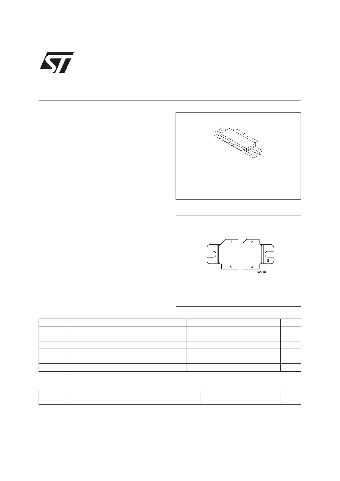
The SD57120 is a common source N-Channel
enhancement-modelateral Field-Effect RF power
transistor designed for broadband commercial
and industrial applications at frequencies up to
1.0 GHz. The SD57120 is designed for high gain
and broadband performance operating in
common source mode at 28V. Its internal
matching makes it ideal for base station
applicationsrequiringhigh linearity.
The
LdmoST
PRELIMINARY DATA
FAMILY
M252
epoxy sealed
ORDERCODE BRANDING
SD57120 XSD57120
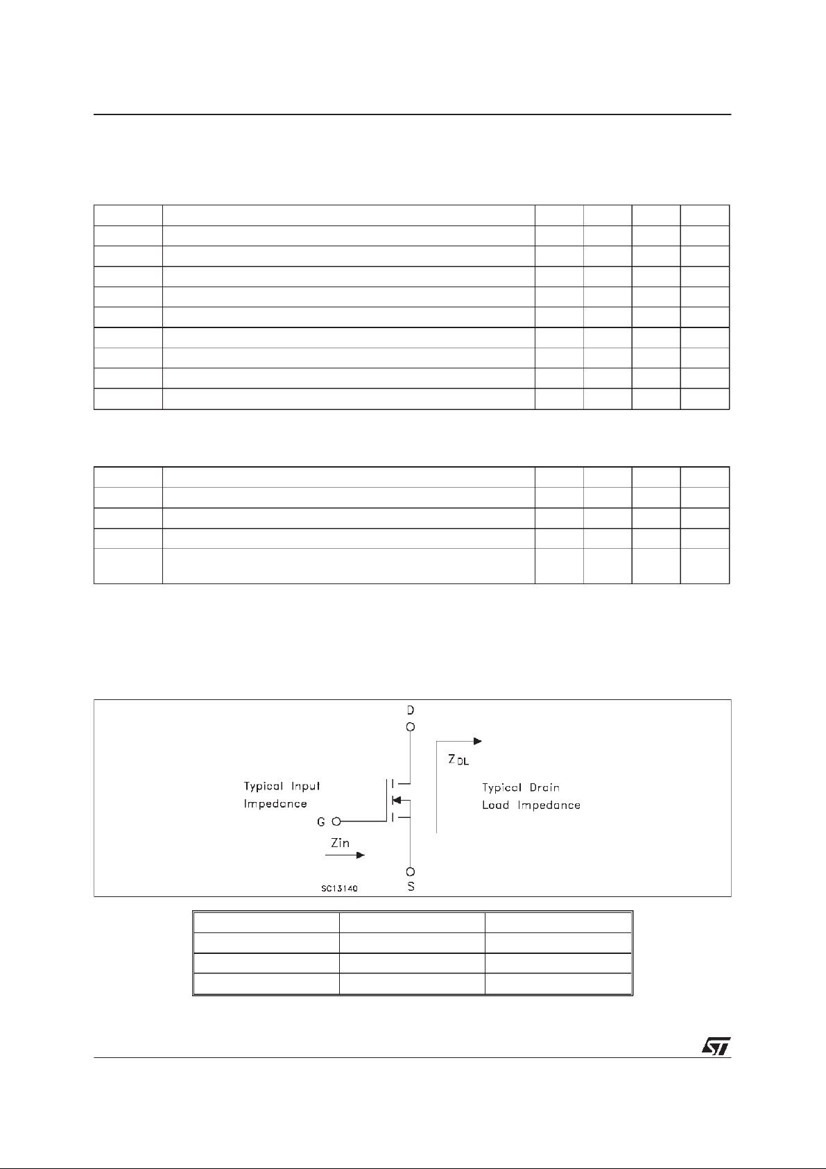
PIN CONNECTION
1. Drain 4. Gate
2. Drain 5. Gate
3. Source
ABSOLUTE MAXIMUM RATINGS (T
Symb o l Parameter Val u e Uni t
V
(BR)DSS
V
P
DISS
T
Drain Sou r ce Volt age 65 V
Gat e- Source Voltage ± 20 V
GS
Drain Current 14 A
I
D
Power Dissipation (@ T c= 70oC) 236 W
Max. Oper ating Junction Tempe r at ure 200
T
j
Storage T emperature -65 to 150
STG
case
=25oC)
THERMAL DATA
R
th(j-c)
March 2000
Junct ion- Ca se Therm al Re sistanc e 0.55
o
o
o
C/W
C
C
1/7
SD57120
ELECTRICAL SPECIFICATION (T
case
=25oC)
STATIC (Per Section)
Symb o l Para met er Mi n . Typ . Max. Uni t
V
(BR)DSSVGS
I
DSS
I
GSS
V
GS(Q)
V
DS(ON)VGS
G
FS
C
*VGS=0V VDS= 28 V f = 1 M Hz 175 pF
ISS
C
OSS
C
RSS
* Includes Internal Input Moscap.
=0V IDS=10mA 65 V
VGS=0V VDS=28V 1 µA
VGS= 20V VDS=0V 1 µA
VDS= 28V ID=100mA 3.0 5.0 V
= 10V ID=3A 0.7 0.8 V
VDS= 10V ID=3A 3 mho
VGS=0V VDS=28V f=1MHz 44 pF
VGS=0V VDS=28V f=1MHz 1.7 pF
DYNAMIC
Symb o l Para met er Mi n . Typ . Max. Uni t
P
OUT
G
η
Load
Mismatch
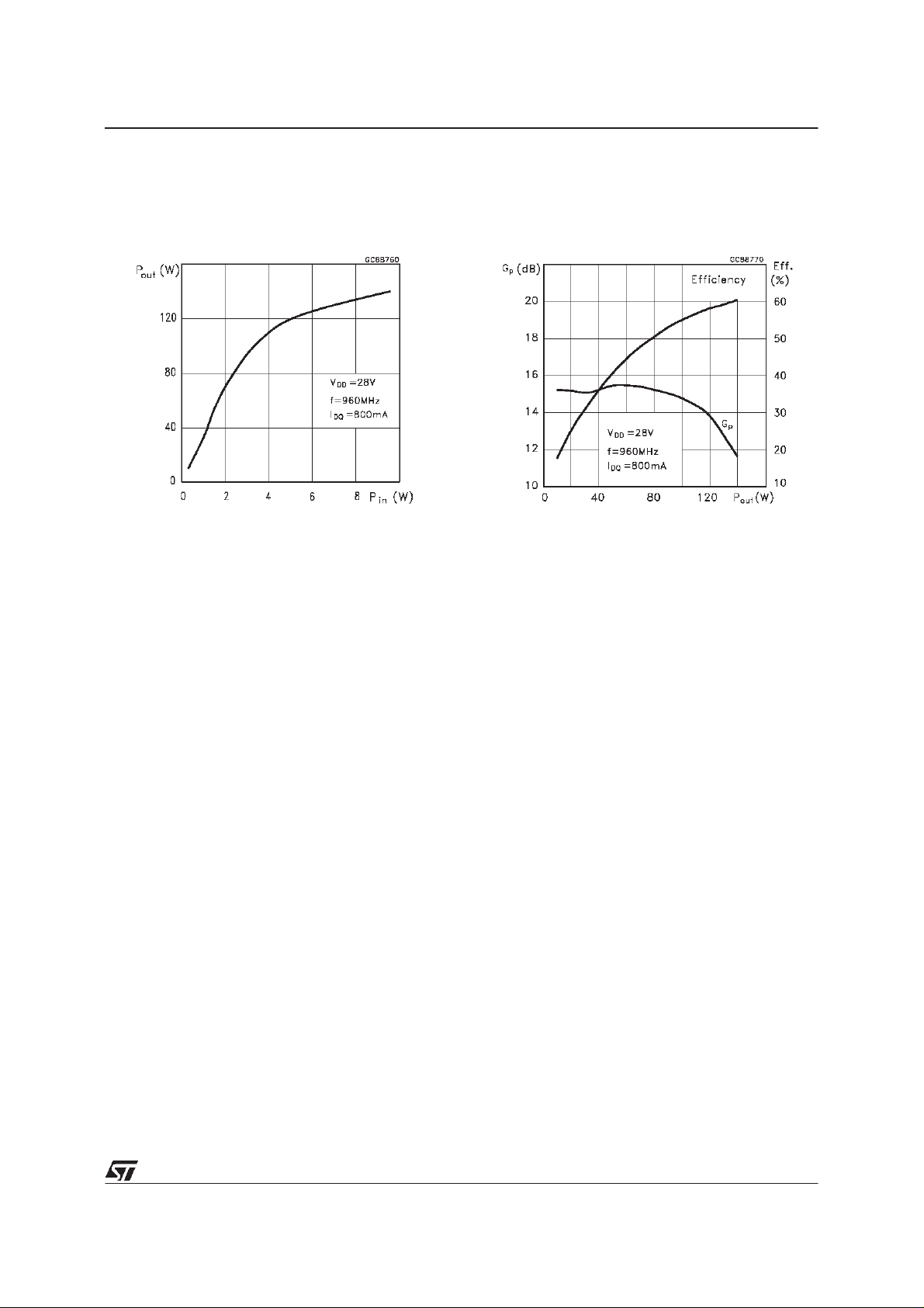
VDD= 28V f = 960 MHz IDQ= 80 0 m A 120 W
VDD=28V P
PS
VDD=28V P
D
f = 960 M H z V
=120W IDQ= 800 mA 13 14 dB
out
= 120W IDQ= 800 mA 50 %
out
=28V P
DD
= 120 W IDQ=800mA
out
10:1 VSWR
ALL PHASE ANGLES
IMPEDANCEDATA
Measured gateto gateand drain todrain respectively.
2/7
FREQ. ZIN(Ω)Z
DL
(Ω)
945 MHz 3.9 + j 4.9 3.6 - j 5.1
960 MHz 4.1 - j 4.6 3.2 4 - j 4. 74
980 MHz 3.9 + j 5.2 3.27 - j 6. 9
SD57120
TYPICALPERFORMANCE
OutputPower vs. Input Power PowerGain and Efficiencyvs. OutputPower
3/7

SD57120
960 MHz TestCircuit Schematic
+
+
C9
C12
R5
C6
960 MHz TestCircuit ComponentPart List
+
C17
L4
C8
C22C19
4/7

960 MHz ProductionTest Fixture
R6
C11
TL1
BALUN1
C12
C10
BF1
L2
C2
C1
L1
BF2
C9
R5
SD57120
C31C29
R4
C20
BF6
BF4
C7
C5
R1
C3
R2
C4
C6
C8
BF3
C14
C35
C15 C16 C18
C17
C13
C34
R3
L3 BALUN2
C23
L4
C19
BF5
C27
C21
C25
C24
TL2
C22
C26
C33
C32
C30C28
5/7

SD57120
M252 (.400 X .800 4L BAL N/HERM W/FLG) MECHANICAL DATA
DIM.
MIN. TYP. MAX. MIN. TYP. MAX.
A 8.13 8.64 0.320 0.340
B 10.80 0.425
C 3.00 3.30 0.118 0.130
D 9.65 9.91 0.380 0.390
E 2.16 2.92 0.085 0.115
F 21.97 22.23 0.865 0.875
G 27.94 1.100
H 33.91 34.16 1.335 1.345
I 0.10 0.15 0.004 0.006
J 1.52 1.78 0.060 0.070
K 2.36 2.74 0.093 0.108
L 4.57 5.33 0.180 0.210
M 9.96 10.34 0.392 0.407
N 21.64 22.05 0.852 0.868
mm inch
6/7
Controllingdimension : Inches
1022783C

SD57120
Information furnished is believed to be accurate and reliable. However, STMicroelectronics assumes no responsibility for the consequences
of use of such information nor for any infringement of patents or other rights of third parties which may result from its use. No license is
granted by implication or otherwise under any patent or patent rights of STMicroelectronics. Specification mentioned in this publication are
subject tochange without notice. This publication supersedes and replaces all information previously supplied. STMicroelectronics products
are notauthorized for use as critical components in life support devices or systems without express written approval of STMicroelectronics.
The ST logo is atrademark of STMicroelectronics
2000 STMicroelectronics – Printed in Italy – All Rights Reserved
STMicroelectronicsGROUP OF COMPANIES
Australia - Brazil - China - Finland- France - Germany - Hong Kong - India - Italy- Japan - Malaysia - Malta - Morocco -
Singapore- Spain - Sweden - Switzerland -United Kingdom - U.S.A.
http://www.st.com
7/7
 Loading...