

RF & MICROWAVE TRANSIST ORS
UHF COMMUNICATIONS APPLICATIONS
.REFRACTORY/GOLD METALLIZATION
.I NTERNAL I NPUT MATCHING
.METAL/CERAMIC PACKAGE
.EMITTER BALLASTED
. 20:1 VSWR CAPABILITY
. P
OUT
25 W MIN. WITH 9 dB GAIN
=
ORDER CODE
SD4013
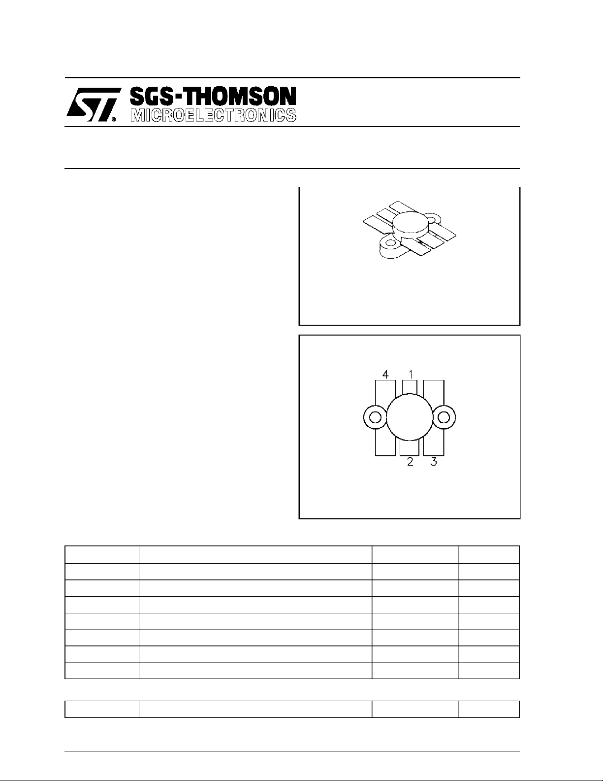
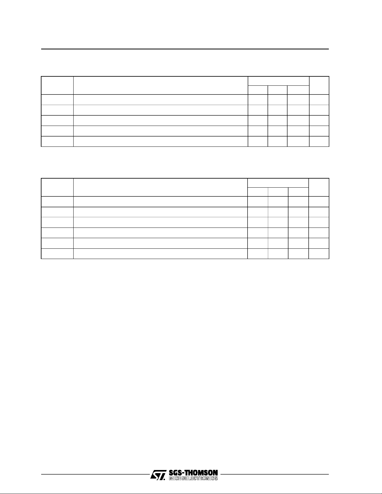
PIN CONNECTION
SD4013
PRELIMINARY DATA
.500 6LF L (M111)
epoxysealed
BRANDING
SUMIL25
DESCRIPTION
The SD4013 is a gold metallized epitaxial silicon
NPN planar transistor using diffused emitter ballast
resistors for superior ruggedness.
The SD4013 canwithstand 20:1 VSWRunder rated
operating conditions andis internally input matched
to optimize power gain and efficiency over the
band.
ABSOLUTE MAXIMUM RATINGS (T
Symbol Parameter Value Uni t
V
CBO
V
CEO
V
EBO
I
C
P
DISS
T
J
T
STG
THERMA L DA TA
R
TH(j-c)
Collector-Base Voltage 60 V
Collector-Emitter Voltage 30 V
Emitter-Base Voltage 3.5 V
Device Current 3.0 A
Power Dissipation 70 W
Junction Temperature +200
Storage Temperature
Junction-Case ThermalResistance 2.5 °C/W
case
= 25°C)
1. Collector 3. Emitter
2. Base 4. Emitter
65 to +150
−
°
C
°
C
November 1992
1/5
SD4013
ELECTRICAL SPECIFICATIONS (T
case
= 25°C)
STATIC
Symbol Test Conditions
BV
CBOIC
BV
EBOIE
BV
CESIC
I
CBO
h
FE
= 50mA IE= 0mA 60 — — V
= 5mA IC= 0mA 3.5 — — V
= 50mA VBE= 0mA 60 — — V
VCB= 30V IE= 0mA — — 3.0 mA
VCE= 5V IC= 500mA 10 30 120 —
Min. Typ. Max.
Value
Unit
DYNAMIC
Symbol Test Conditi ons
P
OUT
P
IN
η
cf=400 MHz VCC= 28V 50 55 — %
G
f = 400 MHz VCC= 28V 25 — — W
f = 400 MHz VCC= 28V — — 3.15 W
f = 400 MHz VCC= 28V 9.0 10.5 — dB
P
Value
Min. Typ. Max.
Unit
VSWR f = 400 MHz VCC= 28V 20:1———
COBf = 1 MHz VCB= 28V — — 30 pF
2/5

TYPICA L PERFO R MA NCE
SD4013
POWER INPUT vs POWER OUTPUT
225 MHz
400 MHz
VCC=28V
POWER OUTPUT vs COLLECTOR
SUPPLY VOLTAGE
f =400 MHz
DC SAFE OPERATING AREA
3/5

SD4013
IMPEDA NCE DATA
TYPICAL IN PU T
IMPEDANCE
Z
IN
TYPICAL COLLECTOR
LOAD IMPEDANCE
FREQ. ZIN(Ω)Z
CL
(Ω)
225 MHz 1.40 + j 2.5 7.55 + j 0.0
275 MHz 1.25 + j 3.3 7.5 − j 0.05
300 MHz 1.10 + j 4.0 7.5 − j 1.00
350 MHz 1.10 + j 4.7 6.8 − j 1.15
400 MHz 1.70 + j 5.1 6.0 − j 1.30
Z
CL
4/5

PACKAGE MECHANICAL DATA
Ref.: Dwg. No. 12-0111
SD4013
Information furnished is believed tobe accurate and reliable. However, SGS-THOMSON Microelectronics assumes no responsability for the
consequences of use of such information nor for any infringementofpatents or other rights of third parties which may results from its use. No
license is granted byimplicationorotherwiseunder any patent or patent rights of SGS-THOMSON Microelectronics. Specificationsmentioned
in this publicationare subject to changewithout notice. This publication supersedes and replaces all information previously supplied.
SGS-THOMSON Microelectronicsproductsare notauthorized foruse ascritical componentsinlifesupportdevices orsystemswithout express
written approval of SGS-THOMSON Microelectonics.
1994SGS-THOMSON Microelectronics- All RightsReserved
Australia - Brazil- France - Germany - HongKong - Italy- Japan - Korea - Malaysia - Malta - Morocco - The Netherlands-
Singapore - Spain - Sweden - Switzerland -Taiwan - Thailand - United Kingdom -U.S.A
SGS-THOMSON Microelectronics GROUP OF COMPANIES
5/5
 Loading...