

.470-860 MHz
.26.5 VOLTS
.GOLD METALLIZATION
.P
OUT
20.0W MIN. WITH 9.5 dB GAIN
=
.I NTERNAL INPUT MATCHING
.DIFFUSED EMITTER BALLAST
RESISTORS
SD4010
RF & MICROWAVE TRANSISTORS
UHF TV LIN EAR APPLIC ATIO NS
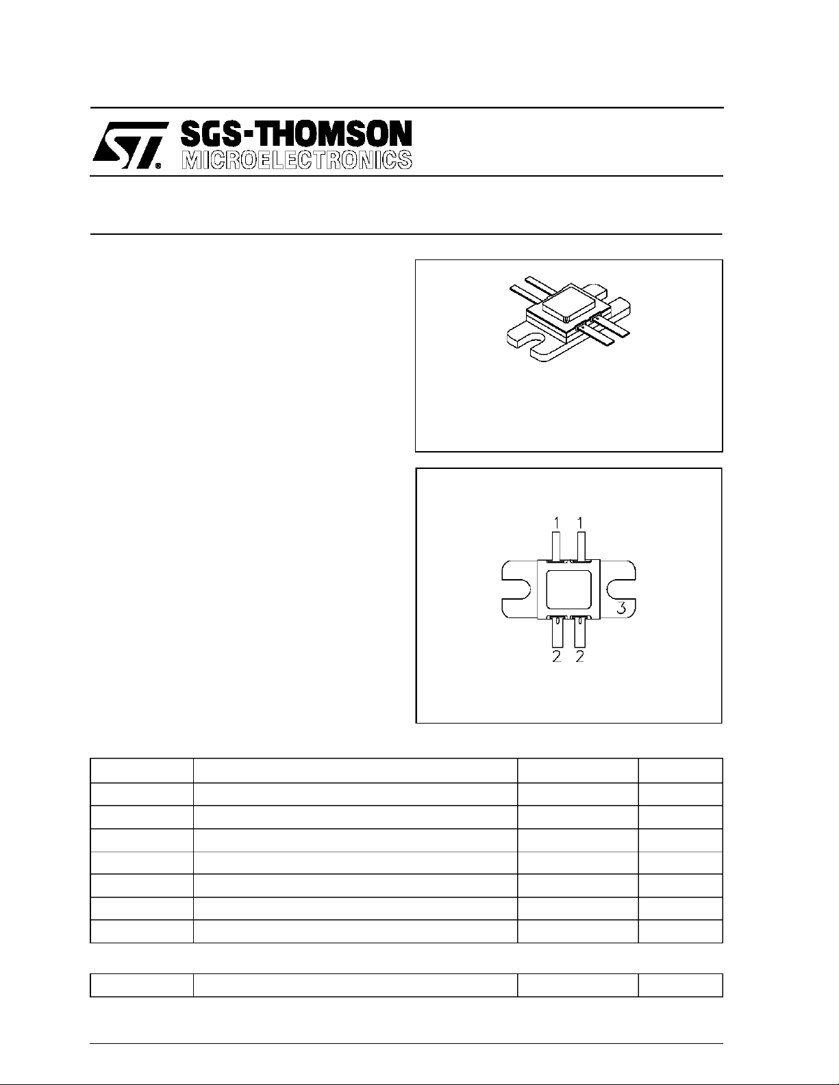
.400 x .425 4L F L (M119 )
hermetically sealed
ORDER CODE
SD4010
PIN CONNECTION
DESCRIPTI ON
The SD4010 is a gold metallized epitaxial silicon
NPN planar transistor using diffused emitter ballast
resistors. The SD4010 is intended for use in linear
applications up to 1GHz, including UHF television
transmitters, transposers and cellular base stations.
ABSOLUTE MAXIMUM RATINGS (Tc ase = 25°C)
Symbol Parameter Value Uni t
V
V
V
P
T
CBO
CES
EBO
I
C
DISS
T
J
STG
Collector-Base Voltage 60.0 V
Collector-Emitter Voltage 60.0 V
Emitter-Base Voltage 4.0 V
Device Current (Maximum) 11.0 A
Power Dissipation 88.8 W
Junction Temperature +200
Storage Temperature
1. Collector 3. Emitter
2. Base
65 to +150
−
BRANDING
SUTV200
°
C
°
C
THERMA L DATA
R
TH(j-c)
November 1992
Junction-Case Thermal Resistance 1.9 °C/W
1/5
SD4010
ELECTRICAL SPECIFICATIONS (T
case
= 25°C)
STATIC
Symbol Test Condi tions
BV
EBOIE
BV
CESIC
BV
CEOIC
I
CEO
h
FE
TestedPer Side
= 10mA IC= 0mA 3.0 4.0 — V
= 50mA VBE= 0V 60.0 85.0 — V
= 50mA IB= 0mA 28.0 30.0 — V
VCE= 26.5V IE= 0mA — — 5 mA
VCE= 5V IC= 3A 25 50 80 —
DYNAMIC
Symb ol Test Co n di t i o ns
P
OUT
G
IMD
IP
C
OB
Load*
f = 860MHz VCE= 26.5V PIN= 2.2W 20.0 28.0 — W
f = 860MHz VCE= 26.5V P
P
P
3
VCB= 26.5V P
3
= 20W VCE= 26.5V (note 1) — −48 −46 dBc
SYNC
= 20W PEP (note 2) — 55 — dBm
OUT
f = 860MHz VCB= 26.5V (note 3) — 25 36 pF
f = 860MHz VCE= 26.5V P
Mismatch
I
I
2.7A (1.3 5A per S ide)
=
CQ
*VSWRtested for a minimumof 3:1 SWR atall phaseangles.
Note1: Three Tone IMD Testing (CCIR)
f
1
f
2
f
3
=
C
860.0MHz/ −8dB ref. to P
=
863.5MHz/ −16dBref. to P
=
864.5MHz/ −7dB ref. to P
=
-Visual
SYNC
- ColorSubcarrier
SYNC
-Aural
SYNC
Value
Min. Typ. Max.
Value
Min. Typ. Max.
= 20W 9.5 10.5 — dB
OUT
= 20W 3:1 10:1 — VSWR
OUT
Note 2: IP3Calculated Based on Two-Tone
Note 3: T es ted Per Side
IMD Testing:
f
900.0 M Hz/−6dB ref. to P
=
1
f
900.1 M Hz/−6dB ref. to P
=
2
IMD3(Typ) <−36dBc
Uni t
Uni t
OUT
OUT
TYPICA L P ERFO R MA NCE
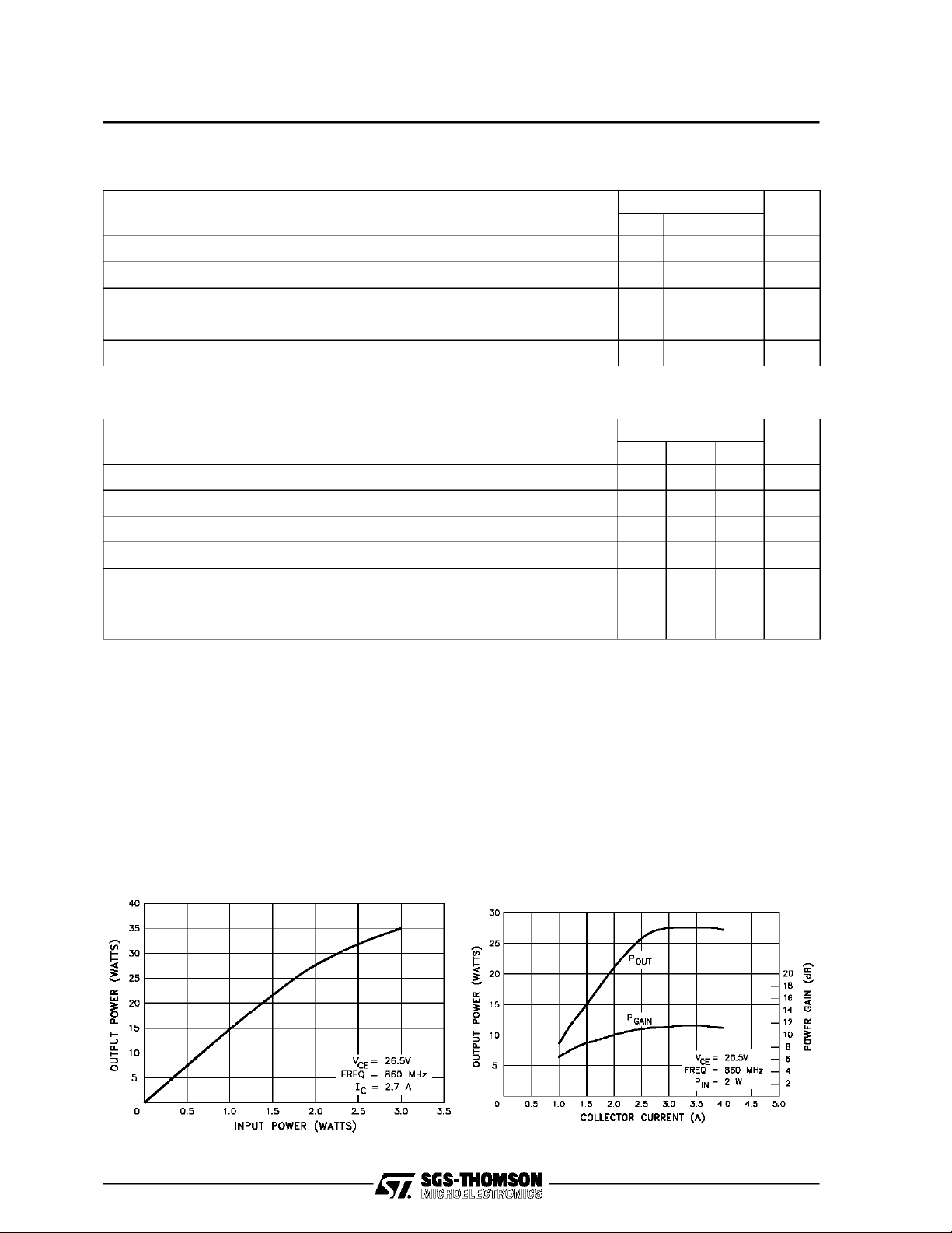
POWER OUTPUT vs POWER INPUT
2/5
POWER OUTPUT & POWER GAIN vs
TOTAL COLLECTOR CURRENT

TYPICAL PERFORMAN CE (c ont ’d )
INTERMODULATION DISTORTION vs POWER OUTPUT
TEST CIRC U IT SCHEMATI C
SD4010
Balun 1, 2 : 50ΩCoaxial Cable,λ/4 @ 860 MHz
C1, C4,
C11, C16 : 100µF, 50V Electrolytic
C2, C5,
C12, C15 : 10µF, 35V Tantalum
C3, C6, C7 C8,
C19, C20 : 75 pF Ceramic Chip, ATC B
C9, C18 : 0.4 - 2.5 pF Variable, JOHANSON Giga-trim
C10 : 2pF Ceramic Chip, ATC B
C17 : 5pF Ceramic Chip, ATC B
L1, L2 : 7 Turns, 0.12” I.D., #22 AWG (1:1)
L3, L4 : 5 Turns, 0.12” I.D., #22 AWG (1:1)
See Photomaster for Microstrip Lines
Board
Material: ROGERS Ultra-Lam Er=2.55, Height=0.030”,
2 oz. Cu.
3/5

SD4010
PHOTO MA STER OF TEST C I RCU IT
4/5

PACKAGE MECHANICAL DATA
Ref. Dwg. No.: 12-0119
SD4010
Information furnished is believed to be accurate and reliable. However, SGS-THOMSON Microelectronics assumes no responsability for the
consequences of use of such information nor for any infringement of patents or other rights of third parties which may results from its use. No
license is granted by implication or otherwiseunderany patent or patent rights of SGS-THOMSON Microelectronics. Specificationsmentioned
in this publication are subject to changewithout notice. This publication supersedes and replaces all information previously supplied.
SGS-THOMSON Microelectronicsproductsare notauthorizedforuse ascritical componentsin life support devices or systems without express
written approval of SGS-THOMSON Microelectonics.
1994 SGS-THOMSON Microelectronics- All RightsReserved
Australia - Brazil - France- Germany - Hong Kong - Italy - Japan - Korea - Malaysia - Malta - Morocco - The Netherlands -
Singapore -Spain - Sweden- Switzerland - Taiwan - Thailand - United Kingdom - U.S.A
SGS-THOMSON Microelectronics GROUP OF COMPANIES
5/5
 Loading...