

®
HF/VHF/UHF N-CHANNEL MOSFETs
■ GOLD METALLIZATION
■ EXCELLENT THE RM AL STABILITY
■ COMMON SOURCE CONFIGURATION
■ POUT = 150W MIN. WITH 14 dB GAI N @175
MHz
DESCRIPTION
The SD2931 is a gold metallized N-Channel MOS
field-effect RF power transistor. The SD2931 is
intended for use in 50V dc large signal
applications up to 230 MHz
SD2931
RF POWER TRANSISTORS
TARGET DATA
M174
epoxy sealed
ORDER CODE BRANDING
SD2931 TSD2931
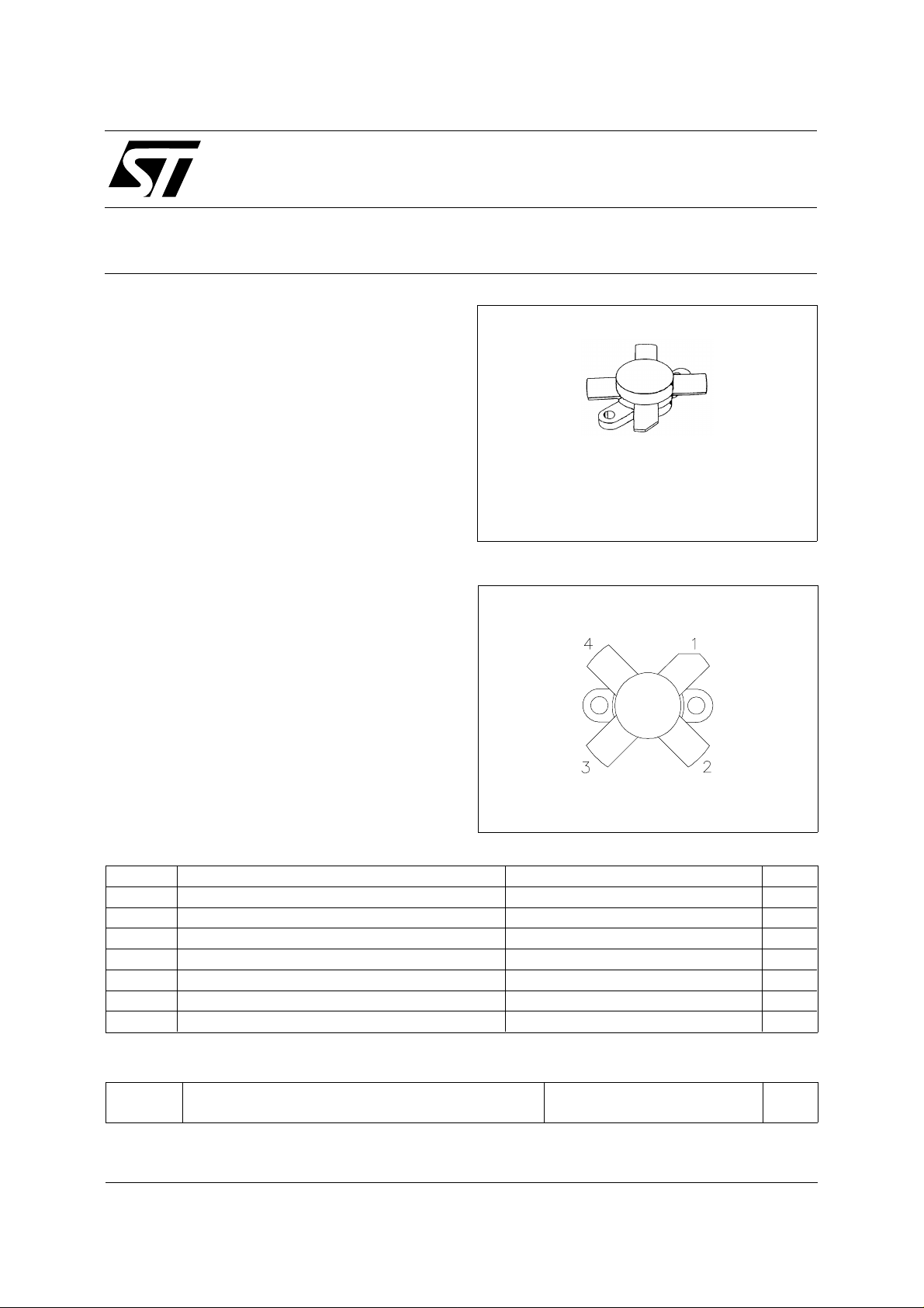
PIN CON NECTION
1. Drain 3.Gate
2. Source 4. Source
ABSOL UT E MAXIMU M RATINGS (T
Symbol Parameter Value Unit
V
(BR)DSS
V
V
P
T
Drain Source Voltage 125 V
Drain-Gate Voltage (RGS = 1MΩ) 125 V
DGR
Gate-Source Voltage ±20 V
GS
Drain Current 16 A
I
D
Power Dissipation 292 W
DISS
Max. Operating Junction Temperature 200
T
j
Storage Temperature -65 to 150
STG
case
= 25 oC)
THERMAL DATA
R
th(j-c)
R
th(c-s)
* Determined using a flat aluminum or copper heatsink with thermal compound applied (Dow Corning 340 or equivalent).
November 1999
Junction-Case Thermal Resistance
Case-Heatsink Thermal Resistance ∗
0.6
0.2
o
o
o
C/W
o
C/W
C
C
1/4
SD2931
ELECTRICAL SPE CIFICATION (T
= 25 oC)
case
STATIC
Symbol Parameter Min. Typ. Max. Unit
V
(BR)DSSVGS
I
DSS
I
GSS
V
GS(Q)
V
DS(ON)VGS
G
FS
C
ISS
C
OSS
C
RSS
= 0V IDS = 100 mA 125 V
VGS = 0V VDS = 50 V 5 mA
VGS = 20V VDS = 0 V 5 µA
VDS = 10V ID = 250 mA 2 5 V
= 10V ID = 10 A 2.7 3 V
VDS = 10V ID = 5 A 5 mho
VGS = 0V VDS = 50 V f = 1 MHz 480 pF
VGS = 0V VDS = 50 V f = 1 MHz 180 pF
VGS = 0V VDS = 50 V f = 1 MHz 15 pF
DYNAMIC
Symbol Parameter Min. Typ. Max. Unit
P
OUT
G
η
Load
Mismatch
f = 175 MHz VDD = 50 V IDQ = 250 mA 150 W
f = 175 MHz VDD = 50 V P
PS
f = 175 MHz VDD = 50 V P
D
f = 175 MHz V
= 50 V P
DD
= 150 W IDQ = 250 mA 14 15 dB
out
= 150 W IDQ = 250 mA 55 65 %
out
= 150 W IDQ = 250 mA
out
10:1 VSWR
All Phase Angles
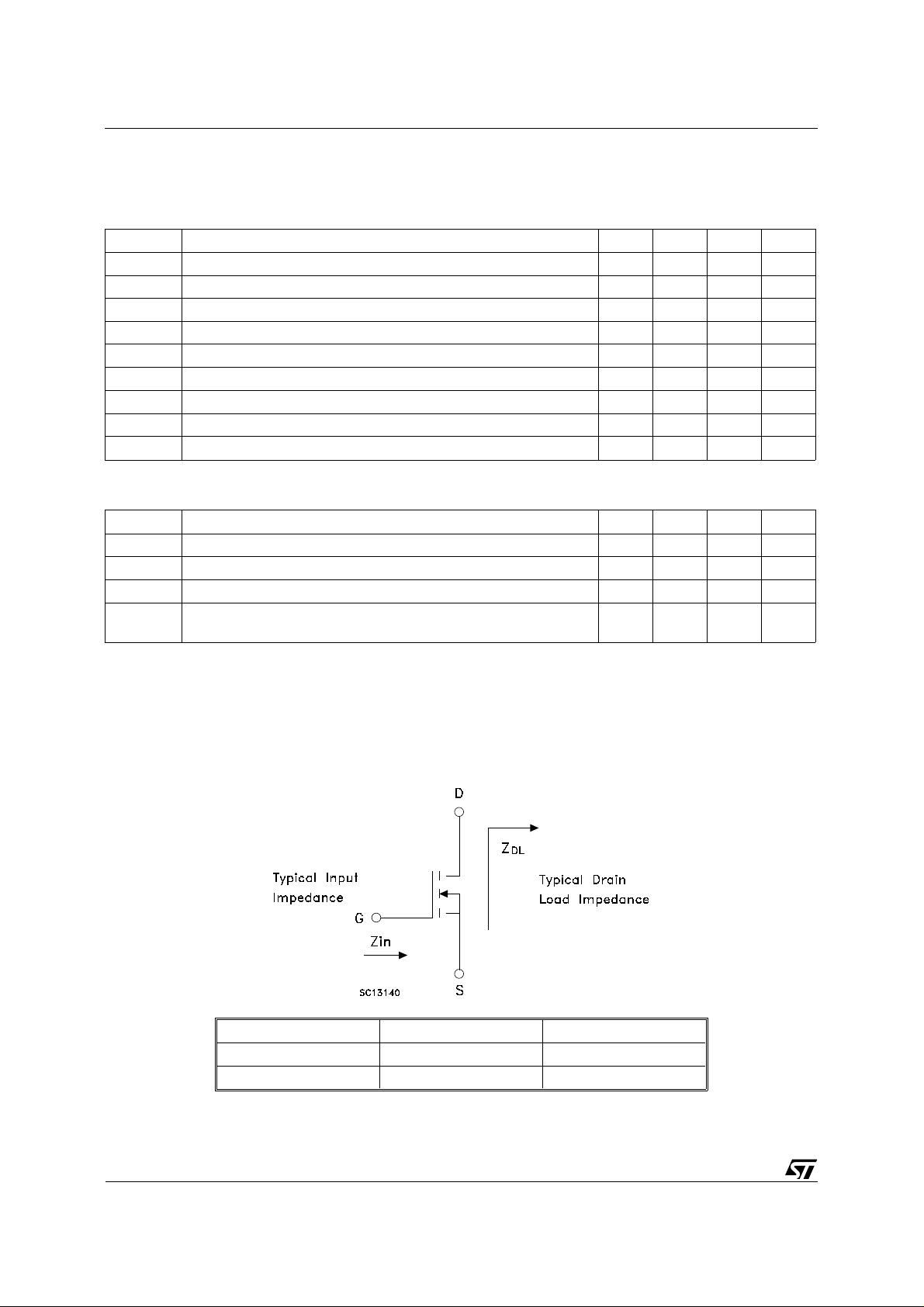
IMPEDANCE DATA
2/4
FREQ. ZIN (Ω)Z
DL
(Ω)
30 MHz 1.7 - j 5.7 6.8 + j 0.9
175 MHz 1.2 - j 2.0 2.0 + j 2.4

M174 (.500 DIA 4L N/HERM W/FLG) MECHANICAL DATA
SD2931
DIM.
MIN. TYP. MAX. MIN. TYP. MAX.
A 5.56 5.84 0.219 0.230
B 3.18 0.125
C 6.22 6.48 0.245 0.255
D 18.28 18.54 0.720 0.730
E 3.18 0.125
F 24.64 24.89 0.970 0.980
G 12.57 12.83 0.495 0.505
H 0.08 0.18 0.003 0.007
I 2.11 3.00 0.083 0.118
J 3.81 4.45 0.150 0.175
K 7.11 0.280
L 25.53 26.67 1.005 1.050
M 3.05 3.30 0.120 0.130
mm inch
Controlling Dimension in Inches
1011000D
3/4

SD2931
Information furnished is believed to be accurate and reliable. However, STMicroelectronics assumes no responsibility for the consequences
of use of such inform ation nor for any infringe ment o f patents or other rig hts o f third par ties which ma y resul t from i ts use. N o li cen se is
granted by implicatio n or otherwise under any patent or patent rights of STMicroelectronics. Specification mentioned in this publication are
subject to change without notice. This publication supersedes and replaces all information previously supplied. STMicroelectronics products
are not authorized for use as critical compo nents in life support devices or systems without express written approval of STMicroelectronics.
The ST logo is a trademark of STMicroelectronics
© 1999 STMicroelectro nics – Printed in Italy – All Rights Reserved
STMicroelectronics GROUP OF COMPANIES
Australia - Brazil - China - Finland - France - Germany - Hong Kong - India - Italy - Japan - Malaysia - Malta - Morocco -
Singapore - Spain - Sweden - Switzerland - United Kingdom - U.S.A.
http://www.st.com
.
4/4
 Loading...